EP0145285B1 - MBE-System ohne Schweissen - Google Patents
MBE-System ohne Schweissen Download PDFInfo
- Publication number
- EP0145285B1 EP0145285B1 EP84307753A EP84307753A EP0145285B1 EP 0145285 B1 EP0145285 B1 EP 0145285B1 EP 84307753 A EP84307753 A EP 84307753A EP 84307753 A EP84307753 A EP 84307753A EP 0145285 B1 EP0145285 B1 EP 0145285B1
- Authority
- EP
- European Patent Office
- Prior art keywords
- chamber
- substrate holder
- wafer
- growth
- retaining ring
- Prior art date
- Legal status (The legal status is an assumption and is not a legal conclusion. Google has not performed a legal analysis and makes no representation as to the accuracy of the status listed.)
- Expired
Links
Images

Classifications
-
- C—CHEMISTRY; METALLURGY
- C30—CRYSTAL GROWTH
- C30B—SINGLE-CRYSTAL GROWTH; UNIDIRECTIONAL SOLIDIFICATION OF EUTECTIC MATERIAL OR UNIDIRECTIONAL DEMIXING OF EUTECTOID MATERIAL; REFINING BY ZONE-MELTING OF MATERIAL; PRODUCTION OF A HOMOGENEOUS POLYCRYSTALLINE MATERIAL WITH DEFINED STRUCTURE; SINGLE CRYSTALS OR HOMOGENEOUS POLYCRYSTALLINE MATERIAL WITH DEFINED STRUCTURE; AFTER-TREATMENT OF SINGLE CRYSTALS OR A HOMOGENEOUS POLYCRYSTALLINE MATERIAL WITH DEFINED STRUCTURE; APPARATUS THEREFOR
- C30B23/00—Single-crystal growth by condensing evaporated or sublimed materials
- C30B23/02—Epitaxial-layer growth
Definitions
- the present invention relates to molecular beam epitaxy (MBE) apparatuses.
- thin film deposition is achieved by directing molecular beams onto a substrate in an ultra high vacuum.
- the beams are not ionized, but are neutral molecular or atomic species, hence the name of the process.
- the substrate is heated to a temperature where kT is large enough to permit a deposited atom to move laterally for an average distance of at least several angstroms, to permit the deposited atoms to find their energetically preferred sites.
- MBE permits growth of thin films with extremely high crystalline quality.
- the MBE technique is generally well known, and has been widely discussed. See, for example, the following review articles, which are hereby incorporated by reference: A.Y. Cho and J.R.
- MBE Molecular beam epitaxy is very attractive as a product technology for many applications, due to its unique capabilities.
- MBE easily produces hetero-epitaxial structures, wherein an epitaxial layer of one material is epitaxially deposited onto an underlying layer of a different material.
- the abrupt epitaxial transitions which can thus be achieved can be rapidly alternated to achieve superlattice structures, wherein, as the different epitaxial layers become very thin, some anomalous and highly desirable properties appear.
- Such structures are very difficult to make in any other way.
- MBE can also be used to make strained superlattices, wherein materials which are not lattice-matched in isolation are nevertheless grown in a perfect epitaxial structure.
- the lattice constant of InAs 0.4 Sb 0.6 is 0.4% less than that of InAs 0.27 Sb 0.73 .
- the two lattices would not be matched.
- the interface between the two materials preserve the crystalline structure of the materials, so that the first lattice is a smooth continuation of the second lattice, except that more arsenic atoms and fewer antimony atoms are now found on the Group V sites.
- MBE also promises other unique capabilities, such as epitaxial deposition of insulators over semiconductors, metals over insulators, etc.
- MBE systems at present are primarily a laboratory tool rather than a production tool, simply because the throughput of MBE systems is slow.
- the slow throughput of MBE systems is unavoidable, since it is difficult to achieve good quality deposited material if the deposition rates used are greater than several microns per hour.
- this problem of slow throughput has been due to the difficulties of wafer handling.
- MBE apparatuses or systems
- molybdenum substrate holders with each wafer being soldered to the substrate holder.
- the actual position of the wafer during MBE growth is downward facing. This is done because, even in an ultra high vacuum system, some particulates will inevitably be present, e.g. particulates which adhere to the inner walls of the chamber until released by thermal cycling, accoustic vibrations, or minor mechanical shocks, and flaky arsenic particles from inadvertent arsenic deposition on the cryoshield. At extremely low pressures these particles will not be suspended in the chamber atmosphere, but will simply fall down to the bottom of the chamber.
- the wafer is positioned facing downward so that it does not intercept the path of any of these falling particulates, and to permit the wafer to face liquid sources such as a liquid gallium source.
- the wafer should be rotated during growth. This provides more uniform deposition and heating.
- an MBE system should have multiple molecular beam sources, to take advantage of the flexibility in deposition discussed above, the molecular beams from most of these sources will not impinge on the wafer at right angles to its surface. Essentially all of the depositions are angle depositions, and rotation of the wafer accordingly improves uniformity.
- Arc-cast molybdenum is an adequately high-purity material for the substrate holder, and can be machined into complex shapes as desired, but unfortunately the thermal expansion coefficient of molybdenum is very different from that of desirable substrate materials, such as gallium arsenide or other III-V semiconductor compounds. This means that the substrate must be held in such a manner that the substrate can expand freely during the temperature rise to the growth temperature, and not be strained by the different thermal expansion of the substrate holder.
- the conventional method of the prior art to accomplish these objectives is indium soldering to a molybdenum substrate holder. That is, a very pure molybdenum substrate holder is used, which includes pins for attachment to the rotating drive in the growth chamber, and the substrate wafer upon which MBE is to be performed is hand-soldered to the substrate holder. That is, the substrate holder is heated to about 1500C on a hot plate, and the wafer is manually placed upon it. At this temperature the indium will be liquid, but will freeze again to provide a good mechanical attachment as the wafer is cooled down. The wafer, mounted to a substrate holder, is then loaded into the MBE system.
- the wafer and substrate holder are eventually transferred into the growth chamber.
- the wafer In the growth chamber, the wafer is held in a downward-facing position, and heated up to the growth temperature. As the wafer temperature increases above the melting point of indium (about 1420C), the indium melts, but the wafer is still held in position by the good adhesive properties of the liquid indium.
- the substrate holder is allowed to cool, so that the indium refreezes and the substrate holder and wafer are then transferred back out of the growth chamber. After the wafer is removed from the MBE system, it is necessary to unsolder it from the substrate holder. This is a very delicate manual step.
- the front surface of the wafer is typically painted with photoresist prior to this etching step.
- the indium on the front side of the emolybdenum substrate holder can be removed by etching the block in HCe.
- this cleanup etch will gradually erode the molybdenum so that the surface of the substrate holder is no longer planar.
- the backside of the wafer is no longer flat. If the wafer is sought to be processed in this condition, very many wafers will be broken during routine handling, since the etched backside will now contain irregularities which can produce local stress maxima. Moreover, use of vacuum chucks in subsequent wafer processing operations now becomes impractical, because the backside of the wafer is no longer flat.
- This difficulty can be mitigated by repolishing the backside of the wafer until it is flat again.
- this provides a further manual processing step, in which further wafer breakage is inherently likely.
- this polishing step will thin them so that they are very fragile and again liable to breakage in routine handling.
- a further difficulty with this prior art method is the smoothness of the molybdenum substrate holder. That is, the substrate holder as received (or as fabricated) will not be perfectly smooth, and the irregularities in the substrate holder surface may themselves make removal of the wafer more difficult. This problem can be avoided by polishing the molybdenum substrate holder, but the problem with this is that repeated polishing of the substrate holder will erode it.
- any processing step which risks slice breakage after the MBE operation has been performed is extremely expensive, since the structure which is thus exposed to a risk of being destroyed may be a structure which has just taken several hours of growth time on a million dollar machine, plus the initial slice cost and the pre-growth slice preparation cost.
- Japanese Patent Publication No. 58-190897(A) discloses a mounting for a substrate to be treated by molecular beam epitaxy consisting of a flat holding plate, consisting of a heat-resistant insulator such as alumina, with a holder of the same material which fits over the rim of the substrate to hold it against the holding plate.
- Another object of the present invention is to provide a method method as defined in claim 16.
- a molecular beam epitaxy apparatus comprising: a growth chamber containing a plurality of effusion sources and a substrate mounting means, means for evacuating said growth chamber to provide an ultrahigh vacuum therein, and means for transferring wafers into and out of said growth chamber, characterised in that the substrate mounting means comprises a substrate holder and a retaining ring being mutually attachable and dimensioned to hold a wafer of predetermined size loosely therebetween around both sides of the periphery only, said substrate holder being detachably fixable to a substrate support within said growth chamber.
- a substrate holder with a lip approximately as high as the thickness of the wafer is used, and a retaining ring attaches to the substrate holder to hold the wafer in place during the growth cycle.
- the retaining ring like the substrate holder, may be made of high-purity refractory material, such as arccast molybdenum.
- the substrate holder and retaining ring are dimensioned to hold the wafer somewhat loosely, to allow for thermal expansion during the cycling up to growth temperature, which is typically about 600 C.
- a problem in conventional MBE systems is outgassing of the sources.
- a conventional MBE evaporation source is a small crucible (in which the source material will be placed), mounted on a vacuum flange together with a resistive heater, a heat shield, and a thermocouple. This structure may contain volatile contaminants, which are likely to escape when the source is heated to the temperatures used for evaporation of the source material.
- the molecular beam epitaxy apparatus may include more than one separate ultra high vacuum chamber. That is, a growth chamber is separated from a sample analysis chamber by a vacuum valve, through which wafers can be passed, and which can be closed to isolate the growth chamber from the analysis chamber.
- the analysis chamber may include a source outgassing fixture, into which one source can be temporarily attached, so that source outgassing can be performed in the secondary chamber, after a wafer has been loaded into the growth chamber, while growth is proceeding in the growth chamber.
- no additional ultra high vacuum facility is required, but source outgassing can be performed with no degradation of throughput.
- a further problem with the throughput of prior art molecular beam systems is the periodic chamber bakeouts which are required. That is, in any ultra high vacuum chamber used for MBE growth, it is necessary not only to bake out the chamber walls after the system has been exposed to air, to remove water and other volatile contaminants, but it is also necessary to periodically bake out the system again, even though the system has not been exposed to air, to again purge the system of contaminants. Volatile contaminants such as arsenic and phosphorus may result from the species used during actual growth period.
- partial bakeouts performed periodically during routine operation, are different from the requirements of full bakeouts.
- it is not necessary to bakeout the whole system evenly.
- the chief problem is due to material which has outgassed from the hot sources and condensed cold chamber walls, so that it is not the sources which need routine periodic bakeouts, but rather the chamber walls.
- contact heating can be used for these partial bakeouts, although use of a heat baffle with radiant heating is still necessary for complete bakeouts whenever the growth chamber has been exposed to the atmosphere.
- Partial bakeout should be performed every week or two, whenever the background pressure of the system, while growth operations are not being performed, begins to rise. This indicates that the pump is becoming loaded by contaminants evaporating from the chamber walls, and a partial bakeout is desirable.
- the MBE apparatus may include an in-place bake out heater. That is, heating tape is preferably wrapped around the growth chamber and the analysis chamber, and left in place, in order to raise the temperature of those chambers to 120 C or so for periodic bakeouts. This permits frequent bakeouts, reducing the partial pressure of water vapor, hydrocarbons, and other undesirable species in the chamber vacuum, and thus enhances growth quality without degrading throughput.
- a further problem of the prior art is that outgassing of the molybdenum substrate holder can never be adequately performed. That is, molybdenum, like many materials, forms a thin layer of native oxides upon contact with the atmosphere. These native oxides cannot be outgassed after a wafer has been mounted. Since a gallium arsenide wafer cannot be heated above about 650 C without degrading the surface quality, it is impossible to outgas the molybdenum adequately when it is in contact with the gallium arsenide wafer. In the prior art, this essentially means that molybdenum substrate holders can never be fully outgassed at all, and will therefore always have native oxides in close proximity to the wafer. Since these native oxides are somewhat volatile, this provides a source of oxygen and oxide impurities which may be transported to the growth front to cause morphological defects in the wafer grown.
- the retaining ring used to affix the wafer to the substrate holder itself has pins on its edge for mechanical manipulation.
- This novel wafer support structure operates together with a vacuum wafer manipulation system, wherein wafers are loaded merely as a cassette of 10 or 20 wafers for MBE growth. After MBE growth has been performed on all of these wafers, the full cassette of wafers is then removed. However, the substrate holder and substrate retainer ring stay in the ultra high vacuum part of the system, and this reduces the number of parts which are cycled from ultra high vacuum into and out of atmospheric conditions.
- the MBE apparatus may have a high vacuum manipulation system, which is embodied in a system having horizontal wafer transport.
- a special wafer cassette is used which has a top shaped to mate with a special substrate holder.
- the cassette is mounted on top of an elevator, i.e. a vertical in-vacuum linear motion element.
- a first fork arm is located so that it can transfer wafers between the substrate holder and the cassette when the substrate holder is located on top of a cassette.
- a second transfer fork is positioned so that it can lift the substrate holder from its position atop the cassette and transfer it.
- a retaining ring holder in the vacuum chamber is connected to a rotary and axial motion feedthrough, and can be used to screw on the retaining ring after the substrate holder has been transferred by the second transfer fork.
- the retaining ring holder contains slots which engage the pins on the retaining ring, so that the retaining ring holder can attach the retaining ring to the substrate holder and can remove the retaining ring from the substrate holder.
- the apparatus can assemble a wafer to its mount in vacuum, and load the wafer thus mounted in its substrate holder onto a transfer fork.
- the transfer fork then transfers the substrate holder and wafer into the growth chamber, wherein the substrate holder is attached to a conventional substrate support with rotary drive.
- MBE system may be arranged in such a way that the transfer of objects into and out of the ultra high vacuum growth chamber is minimized.
- the MBE system may further include means for wafer loading and unloading onto the growth site which can be automatically controlled.
- MBE molecular beam epitaxy
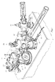
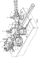
- FIG. 1 shows generally an MBE system which may embody the present invention.
- the system in this embodiment, consists of three separate vacuum chambers, with valves interconnecting them.
- a growth chamber 10 is the vacuum chamber in which actual thinfilm deposition occurs.
- Mounted on this chamber are a plurality of sources 12, (effusion cells of Knudsen type).
- Each source 12 normally includes a shutter, so that, to deposit a selected species or combination of species, the operator can supply drive current to the resistive heating elements in the desired sources 12 and unshutter them to provide molecular beams under ultra high vacuum conditions.
- a substrate holder 14 is positioned downwardly facing and generally facing these sources 12, so that when the sources 12 emit molecular beams they will impinge on the substrate holder and can be incorporated in film growth.
- the substrate holder 14 normally incorporates a resistive heating element, and is connected to a rotary drive 18 so that the substrate holder 14 can be continuously rotated during the growth process, to promote more uniform growth.
- the inside of the growth chamber 10 is lined with a cryo shield, which includes plumbing connected to external liquid nitrogen supply and exhaust parts 22 and 23. During growth, the cryo shield is cooled to approximately 77 degrees K, to reduce background contaminants during growth.
- the rotating substrate support 14 normally remains in the chamber. However, a substrate holder 24 can be mounted and dismounted from a substrate support 14 under vacuum. This substrate holder 24 will typically have a wafer 26 attached to it.
- the growth chamber 10 is separated from an analysis chamber 28 by a valve 30.
- the valve 30 must be capable of withstanding ultra-high vacuum without leakage to the outside world. Note that the valve 30 is preferably not placed where it can see the sources 12, to avoid plating excessive amounts of the molecular beam species onto the valve. Alternatively, a shutter could be placed in front of the valve.
- a first transfer arm 32 is aligned with the valve 30, so that the first transfer arm 32 can transfer a wafer 26 and a substrate holder 24 from the growth chamber 10 to the analysis chamber 28 and back.
- the analysis chamber 28 will typically include analysis equipment so the condition of the grown film can be inspected without exposing it to atmospheric contamination.
- the analysis equipment may typically include instruments such as Auger analyzer, ESCA (electron spectroscopy for chemical analysis) analyzer, SIMS, etc.
- the growth chamber 10 is equipped with its own high vacuum pump (e.g. an ion pump), and the analysis chamber 28 has its own high vacuum pump 38. Similarly, the preparation chamber has its own vacuum pump 40.
- the growth chamber and analysis chamber will typically both be operated at pressures in the neighborhood of 1E-11 Torr, whereas the preparation chamber, which is frequently opened to the atmosphere, is normally operated at pressures only around 1E-8 Torr.
- a second valve 42 similar to the valve 30, connects the analysis chamber 28 to the preparation chamber 44, and a second transfer arm 46 is positioned in line with the valve 42 to transfer wafers and substrate holders from the preparation chamber 44 into the analysis chamber 28.
- the vacuum feedthrough for the second transfer arm 46 is essentially the same as that for the first transfer arm 32.
- the preparation chamber 44 While the valve 42 is closed, the preparation chamber 44 is opened to the atmosphere, and 3 wafers, each assembled to a substrate holder and retaining ring, are loaded into the preparation chamber.
- One substrate holder is affixed to the slots on the end of the second transfer arm 46, which are positioned to engage the pins around the circumference of the substrate holder, and the other 2 substrate holders are similarly engaged by slots in the first wafer carrier 45.
- the preparation chamber 44 is then closed, and a rounting pump then brings it down to an initial low pressure.
- the preparation chamber 44 is then connected to ion pump 40, and brought down to a reasonable vacuum, e.g. 1E-8 Torr.
- one of the positions on the wafer mount 45 is provided with a heater, so that a wafer can be outgassed at low temperature (e.g. 200 C) to minimize contamination of the high vacuum chambers.
- low temperature e.g. 200 C
- the valve 42 is opened, and second transfer arm 46 transfers the wafer it is holding to the second wafer carrier 29 in the analysis chamber 28.
- This second transfer arm 46 is then retracted, the wafer carrier 45 is rotated so that the wafer which has just been outgassed is facing the transfer arm 46, the transfer arm 46 engages the substrate holder around this wafer, the wafer carrier 45 is rotated again so that the transfer arm 46 can pass through, and the transfer arm 46 again reaches into the analyzes chamber to place this outgassed wafer onto the second wafer carrier 29.
- the second transfer arm is then retracted, and the valve 42 is closed.
- the second transfer arm 46 now loads another wafer onto the heated position of the wafer carrier 45 for outgassing. Meanwhile, depending on the substrate used, an ion bombardment step may now be performed in the analysis chamber 28 to clean the surface of the wafer for growth.
- the second wafer carrier 29 is then rotated so that the wafer to be grown faces the first transfer arm 32, and the first transfer arm 32 is extended and rotated to pick up the wafer next to be grown.
- the second wafer carrier 29 is rotated so that the first transfer arm 32 can pass through it, and the valve 30 is then opened so that the first transfer arm can reach into the growth chamber.
- the substrate support is now rotated so that it faces the first transfer arm, and the first transfer arm is extended into the growth chamber where it attaches the growth wafer by a rotary motion to the substrate support.
- the cryo shield will be supplied with liquid nitrogen, so that its temperature is approximately 77K.
- the first transfer arm 32 will then be retracted and the valve 30 closed, and preparations for growth can begin. That is, the substrate support will now be rotated into the growth position, which in the presently preferred embodiment faces downward along an axis approximately 221 ⁇ 2 degrees from horizontal.
- the arsenic source will be powered to provided a background arsenic pressure of about 1E-5 Torr of arsenic in the growth chamber. While this arsenic overpressure is maintained, the heating filament in the substrate support will very briefly be powered sufficiently to run the wafer up to a temperature of about 630 C.
- the wafer is then returned to a steady state growth temperature, of 600 C in this example, and the desired sources for epitaxial growth are powered up and unshuttered. After the desired growth has been achieved, the arsenic cell only is left open, to again provide an arsenic overpressure of about 1E-5 Torr, while the wafer cools. After the wafer is cooled, the arsenic source is shuttered, and the above sequence of wafer transfers is repeated in reverse.
- the end of such a sequence of operations is a set of 3 wafers, each still mounted between a substrate holder and a retaining ring and each having an epitaxial layer thereon, in the preparation chamber 44.
- Preparation chamber 44 is then opened to atmosphere, the grown wafers are removed, and new wafers, each in a substrate holder and a retaining ring, are mounted.
- the wafer is heated to a temperature (e.g. 600 C) sufficient to provide surface mobility for the as-deposited atoms for them to seek out their energetically favorable lattice positions, thus assuring good lattice quality.
- a temperature e.g. 600 C
- the temperature of the wafer 26 during growth must be carefully monitored. This can be done in at least 2 ways.
- an optical pyrometer 48 is used. This instrument looks through a view port in the wall of the growth chamber 10 so that it can see the wafer 26 during growth. Preferably the viewport is shuttered most of time, to eliminate the deposition of reflective films on the viewport.
- thermocouple can be mounted on substrate 14 in close proximity to the backside of substrate holder 24.
- a resistive heating element is also incorporated in the substrate support 14, close to the backside of the substrate holder 24.
- the substrate holder 24 is preferably made quite thin, to maximize the thermal coupling between the wafer 26 and heater element.
- the ultrahigh vacuum analysis chamber reduces contamination of the growth chamber vacuum, and also permits the condition of a wafer to be inspected exactly as it is grown. However, although these functions are extremely important, it should be noted that the analysis chamber is not typically actually being used for anything during the growth run for each wafer.
- a source outgassing mount 50 is provided on the analysis chamber 28.
- the source outgassing mount 50 is preferably a cylinder long enough that a source 12 which is temporarily mounted in the source outgassing mount does not actually protrude into the analysis chamber.
- the resistive heater in the source is activated, to heat the source to at least about 1400 C for at least several dozen hours. This outgassing step removes a large part of the residual impurities which would otherwise be baked out of the crucible during the actual source evaporation step.
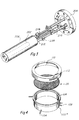
- FIG. 3 A sample molecular beam source (Knudsen effusion cell) of the prior art, as used in this arrangement, is shown in Figure 3. That is, a crucible 202 is supported inward from a vacuum flange 204, and is surrounded by a heat shield 206. The crucible is heated by a resistive heater 208, and its temperature is sensed by thermocouple 210. An electrical feedthrough 212 is provided for the resistive heater, and a separated electrical feedthrough 214 is provided for the thermocouple.
- the source outgassing mount 50 incorporates a cooling tube 52.
- a cooling tube 52 which is thermally connected to the source outgassing mount 50.
- the cooling tube 52 is connected to the liquid nitrogen exhaust 23 from the cryo shield in the growth chamber. That is, it is not critical that the source outgassing mount 50 be held at exactly 77 K, so that the cold nitrogen from exhaust port 23 can be used again to reduce the temperature of the cooling tube 52 which is in close proximity to the high temperature source 12.
- the source is demounted from the source outgassing mount 50 when next the preparation chamber 44 is open to atmosphere, and the source is reloaded with the source material.
- an indium source would be reloaded with a small ingot (e.g. 50 grams) of indium of the highest attainable purity.
- the source 12 is then preferably mounted again on the source outgassing mount 50, and, after the system has been pumped down and a new wafer 26 has been loaded into the growth chamber 10 and growth is proceeding, the source is again outgassed.
- the second optional outgassing step is performed at a temperature which is merely 50 degrees above the evaporation temperature of the source.
- an aluminum source would typically be operated at a temperature of about 1000 C, and this source would therefore be outgassed at a temperature of 1050 C.
- an arsenic source would typically be operated at a temperature of only 250 C, and this source would therefore be outgassed at a temperature of only 300 C.
- the source outgassing mount 50 need not have this physical configuration.
- the source outgassing mount 50 need not look directly into the analysis chamber, but a baffled connection may be provided, to catch more of the high temperature species emitted from the source during outgassing.
- the source outgassing mount 50 could be made longer, to physically remove the high temperature source even farther from the analysis chamber 28.
- the analysis equipment 34 will typically be shuttered during the actual outgassing operation.
- a valve or shutter could also be interposed between the source outgassing mount 50 and the analysis chamber 28, to minimize stray contaminants during wafer transfer and the analysis operations.
- the principal teaching is that, in a molecular beam epitaxy system which includes an ultrahigh vacuum growth chamber and also another ultrahigh vacuum chamber, the second ultrahigh vacuum chamber incorporates a source outgassing mount, so that sources can be outgassed in ultrahigh vacuum while a growth operation is proceeding.
- this source outgassing mount is cooled with the exhausted cryogenic gases from the cryo shield in the main growth chamber.
- a source outgassing mount is located on a high vacuum chamber which is part of the system but which is not the growth chamber, for the protracted outgassing of sources which is desirable.
- the source outgassing mount 50 could be mounted on the preparation chamber 44 rather than on the analysis chamber 28.
- the source outgassing mount 50 is preferably closer to the ion pump in the analysis chamber than is the wafer transfer path, i.e. than the wafer carrier 29 and the paths of the transfer arms 32 and 46. That is, in the sample configuration of Figure 1, a high vacuum pump, such as an ion pump or a tubornolecular pump, is preferably located below the analysis chamber 28, although this is not separately shown. This means that the new source mounted on the source outgassing mount 50 can be left at high temperature continouously during wafer transfer operations, since the contaminants outgassed from the new source, if not collected on the cooled walls of the source outgassing mount 50, will probably diffuse downward toward the vacuum pump rather than upward toward the wafers located in the chamber.
- a high vacuum pump such as an ion pump or a tubornolecular pump
- an initial bakeout is necessary. This is normally performed by enclosing the growth chamber 10 within a bake out oven, i.e. a heat shield incorporating radiant heaters, which can heat the whole growth chamber 10 to about 200 C. During this operation, it is of course necessary to disconnect the cryogenic gas connections, and also, to fit the furnance in place, it is normally necessary to disconnect other elements, including other electrical and plumbing connections.
- a bake out oven i.e. a heat shield incorporating radiant heaters
- growth chamber 10 is provided with a resistive heater, such as a heater tape 54, which is permanently left in place, wrapped all around the growth chamber, to provide partial bake outs during operation. That is, this heater tape can provide a bakeout at 110 or 120 C, which is adequate to desorb much water, phosphorous, and arsenic from the chamber walls. Preferably this bakeout is performed overnight.
- a resistive heater such as a heater tape 54, which is permanently left in place, wrapped all around the growth chamber, to provide partial bake outs during operation. That is, this heater tape can provide a bakeout at 110 or 120 C, which is adequate to desorb much water, phosphorous, and arsenic from the chamber walls. Preferably this bakeout is performed overnight.
- the heating tape presently used is about 30 feet long, and provides a heating power of about 30 watts per foot.
- this tape is wrapped in aluminum foil, to spread the heat flow into the vacuum chamber walls.
- a wide variety of other heating means could be used.
- the principal teaching of this novel aspect of the invention is that the growth chamber of an MBE system is provided with permanently located heating means, so that it is not necessary to remove appurtenances in order to attach a heating furnance for partial bakeout.
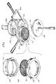
- Figure 2 shows the attachment of a wafer 26 and substrate holder 24 to the substrate support 14. This structure is located inside the growth chamber 10, and is attached to the wafer drive 18.
- the substrate holder of the prior art uses a holder 102 of high-purity molybdenum, which has pins 104 attached to its periphery. The pins 104 provide the attachment for the substrate support 14. These pins 104 are held by forks 106 driven by the wafer drive 18, to rotate the substrate holder 102 during growth.
- the prior art method of attaching the wafer 26 to the substrate holder 102 is by indium soldering.
- the substrate holder 102 is given a different structure, which permits a different attachment method.
- the novel substrate holder 102 still has pins 104 which are driven by the forks 106 of the substrate support 14, but the substrate holder 102 also has additional pins 108. These additional pins 108 engage slots 110 in a retainer ring 112. As seen in Figure 4, the slots 110 in the retainer ring 112 engage the pins 108 on a substrate holder 102, so that the wafer is held there between. Note that the substrate holder 102 has raised lip 114 on its face, so that the wafer 26 is held slightly loosely between the substrate holder 102 and the retainer ring 112. It is necessary that a percent or two of extra space be present in these dimensions, to allow for thermal mismatch.
- the substrate holder 102 is provided with a thin back, for good thermal coupling of the wafer 26 to a resistive heater in the substrate support 14.
- a boss is provided centered in the back of the substrate holder, so that a thermocouple located in the substrate support 14 can accurately sense the temperature of the substrate holder 102 and therefore of the wafer 26.
- this boss may be omitted if an optical pyrometer is used to sense the temperature of the wafer during growth, as is presently preferred.
- the substrate holder itself has no back. As shown in Figure 4, this configuration still provides good mechanical support for the wafer 26. This arrangement provides even better thermal coupling of the wafer 26 to a resistive heating element.
- the retainer ring 112 is modified slightly.
- the modified retainer ring 112' includes not only slots 110, but also pins 320, around its peripbery. These pins 320 mean that assembly of the retainer ring to the substrate holder 102' need not be done manually, but can be done in the vacuum chamber using manipulators, which are either manually controlled by feedthroughs or are automatically controlled.
- This novel structure provides a whole novel mode of wafer handling operations for molecular beam epitaxy systems, which will now be discussed.
- this novel aspect of the invention provides still a different substrate holder 102'', together with a modified retaining ring 112'.
- a special cassette 302 is also provided.
- the substrate holder 102'' and the retainer ring 112' stay in ultrahigh vacuum, and only the wafers 26 are transported into and out of the MBE system.
- a substrate holder structure is provided which can be assembled and disassembled within an ultrahigh vacuum chamber by manipulators controlled from outside of the vacuum.
- the cassette 302 has slots 304 in its side to hold a number of wafers 26.
- the top of the cassette 302 includes a wide slot which mates with the substrate holder 102, so that the substrate holder 102'' can easily be lifted off of the cassette 302 but will not turn while it is in place atop the cassette.
- the presently preferred embodiment of this aspect of the invention is based on a Perkin-Elmer MBE system, which incorporates numerous other minor differences from the system discussed above.
- the wafer is held during growth not by pins around the periphery of the substrate holder, but by internal expanding fingers which grip the inside of the substrate holder from its back.
- a sample introduction chamber 402 is the chamber into which a cassette 302 filled with 10 or 20 wafers 26 is originally loaded. After the cassette is loaded and the introduction chamber 402 pumped down, the valve which vertically separates the wafer introduction chamber 402 from the wafer storage chamber 404 is opened, and an elevator 306 (i.e. a vertical linear motion element) located within the storage chamber 404 supports the cassette 302 and then lowers it down into the storage chamber 404.
- an elevator 306 i.e. a vertical linear motion element
- the cassette 302 is positioned on top of an elevator 306 in the storage chamber.
- This elevator 306 provides the vertical motion, so that the transfer arms 432 and 446 need only to provide lateral motion.
- the substrate holder 102 which is being held by first transfer arm 432, is placed on the cassette 302. (Note that the substrate holder 102'' has never been exposed to atmosphere.)
- arm 432 is retracted, the elevator 306 is raised, a second transfer arm 446 reaches into one of the slots 304, and the cassette 302 is lowered slightly so that one particular wafer 26 is resting on the fork on the end of the second transfer arm 446.
- This arm is then retracted, the cassette is lowered, and the arm is extended again so that the wafer is above the recess in the top of the substrate holder 102''.
- the substrate holder 102'' has not only a recess to hold a wafer, as described above, but also has slots 308 in it into which the fork on the end of the second transfer arm 446 can reach. These slots preferably have a slight lead-in taper (as slot 312 preferably does too), to provide mechanical positioning and to compensate for any slight lateral slot in control of the transfer operations.
- the substrate holder 102'' also has linear rabbets 310 cut in the shoulder of its lower surface, so that the substrate holder 102'' mates with wide slot 312 in the top of the cassette 302.
- At least two of the rabbets 310 in the substrate holder 102'' reach high enough that they not only can mate with a wide slot 312 on top of the cassette 302, but also provide a clearance for the fork on the end of the first transfer arm 432 to reach in and lift the substrate holder 102'' so that it is prevented from turning.
- the substrate holder 102'' is then carried by the first transfer arm 432, to the analysis chamber 408, where the retaining ring 112' is assembled to the substrate holder 102''.
- the retainer ring 112' still has slots 110, which mate with pins 108 on a substrate holder 102'', but the retainer ring 112' also has additional pins 320. These pins 320 mate with T-shaped slots 324 in a retainer ring holder 322.
- these T shaped slots 324 in the retaining ring holder 322 permit the holder 322 to grasp the retainer ring 112', to rotate it in either direction, and to lift it.
- the holder 322 has its own rotary and axial feedthrough, and is located in the analysis chamber.
- the holder 322 can be located anywhere along the path of arm 432.
- the holder 322 can be aligned with the elevator 306 in the storage chamber, and therefore the holder 322 would need to be connected only to a rotary feedthrough, and not to an axial feedthrough. In this case, a mechanism for lateral cassette transport must be used.
- the retaining ring holder 322 assembles the retaining ring 112' to the substrate holder 102'' enclosing a wafer 26 therebetween, after the first transfer arm 432 has lifted the substrate holder 102'' from the top of the cassette 302.
- wafer transfer proceeds as discussed above. That is, the assembled wafer and substrate holder are transferred in vacuum into the growth chamber 10, and now can be mounted onto the substrate holder 24, which is driven by the wafer drive 18 during the growth stage.
- the above operations are repeated in reverse. That is, the substrate holder 102'' is removed from the growth chamber through the valve 30, the retainer ring holder 322 removes the retaining ring 112' from the substrate holder 102'' and holds it, the substrate holder 102'' is placed in the wide slot 312 on the cassette 302, and the second transfer arm 46 removes the wafer 26 from the substrate holder 102'' and places it into an empty slot 304. The second transfer arm 46 then removes an ungrown wafer from one of the slots 304, and the cycle repeats. After all wafers have been grown, the entire cassette 302 is removed by the elevator 306 arm 46 into the introduction chamber, whence it can be manually unloaded.
- the substrate holder 102'' due to the provision of rabbets 310 and slots 308, is necessarily thicker than the substrate holder 102 or 102'. Note that the substrate holder 102'' is preferably backless, to permit better thermal coupling of the wafer 26 to a resistive heater.
- the substrate holders 102 or 102' or 102'', and the retaining rings 112 or 112', are all preferably made of high purity arccast molybdenum. However, other materials which can readily be formed into complex shapes and which are not prone to outgassing of volatile contaminants can be used instead.
- the cassette 302 It is not, of course, strictly necessary that the cassette 302 have a wide slot 312 to mate with substrate holder 102''. This is the preferred arrangement, which provides an economical configuration of elements.
- a mechanical engagement of the substrate holder 102'' with the wide slot 312 on top of the cassette 302 is also advantagous, as described above, since this provides a mechanical constraint on the relative positions of the substrate holder 102'' and the cassette 302. This simplifies control operations, and obviates any need for a second axis of motion to be provided on the transfer arms 432 or 446.
- a wide variety of other mechanical arrangements could of course be used.
- a substrate holder and retaining ring are provided, which are dimensioned to provide a space therebetween which is approximately equal to (preferably slightly larger than) the dimensions of a wafer on which MBE growth is to be performed.
- a simple attachment between the substrate holder and retaining ring is provided which can be assembled by a very simple mechanical motion, such as pins engaging T-shaped or helical slots.
- the substrate holder and retaining ring are provided with surface shapes to permit assembly by a simple mechanical manipulation, such as pins on the retaining ring and rabbets on the substrate holder.
- the result of these teaching is to permit a mode of operation wherein the substrate holder and retaining ring both remain in vacuum while a cassette of grown wafers is unloaded into atmospheric pressure, and while a new cassette of ungrown wafers is loaded from atmospheric pressure, pumped down, and transferred into the high vacuum parts of the system.
- a cassette full of wafers is placed into an introduction chamber, which contains an elevator and is accessed by a second transfer arm 446, which operates as discussed above to transfer unmounted wafers onto a substrate holder 102''.
- a first transfer arm 432 transfers the substrate holder 102'' to a second chamber, where a retaining ring holder 322 assembles a retaining ring 112' to the substrate holder 102'', as described above.
- the arm 432 then transfers the wafer (assembled to its substrate holder and retaining ring) onto a rotatable wafer carrier in third chamber.
- This rotatable wafer carrier is rotated to put the wafer in a vertical orientation, and the substrate holder can now be grasped by another transfer arm 32 which carries the wafer, in a vertical position, into an analysis chamber and a growth chamber.
- one advantage of this system configuration is that it possible to outgas the molybdenum substrate holder and retaining ring thoroughly, without a wafer being present.
- a new substrate holder and retaining ring when first loaded, they can be baked out at as high a temperature as desired for as long as desired, e.g. at 1000 C for 6 hours. After this initial bakeout, the molybdenum will not reform native oxides, since it will not be exposed to any high partial pressure of oxygen.
- the retaining ring will gradually accumulate deposited material from the beam sources, and eventually must be exchanged.
- a further advantage of the present invention is that it not only provides reduced cycling between the growth chamber pressure and atmospheric pressure, but it also permits automation. That is, the transfer operations required to assemble the wafer to the substrate holder which are all preferably performed (in this embodiment) by invacuum motors controlled by electrical feedthrough, or by a stepper motor connected through a vacuum bellows to the transfer arm 446, can be controlled by a conventional programmable controller, so that it would not be necessary to have an operator present. Thus, the machine could operate unattended for a number of consecutive growth runs under automatic control.
Landscapes
- Chemical & Material Sciences (AREA)
- Engineering & Computer Science (AREA)
- Crystallography & Structural Chemistry (AREA)
- Materials Engineering (AREA)
- Metallurgy (AREA)
- Organic Chemistry (AREA)
- Physical Deposition Of Substances That Are Components Of Semiconductor Devices (AREA)
- Crystals, And After-Treatments Of Crystals (AREA)
Claims (16)
- Molekularstrahl-Epitaxievorrichtung, mit einer Aufwachskammer (10), die mehrere Effusionsquellen (12) und ein Substrathaltemittel (14, 102, 112) enthält, Mitteln (angeschlossen an 22; 23) zum Evakuieren der Aufwachskammer, um in dieser ein Ultrahochvakuum zu erzeugen, und Mitteln zum Überführen von Scheiben in die und aus der Aufwachskammer, dadurch gekennzeichnet, daß das Substrathaltemittel einen Substrathalter (102) und einen Festhaltering (12) enthält, wobei der Substrathalter und der Festhaltering aneinander befestigbar und so dimensioniert sind, daß eine Scheibe (26) mit vorbestimmter Größe lose zwischen ihnen nur um beide Seiten des Umfangs gehalten werden, wobei der Substrathalter lösbar an einem Substratträger (14) innerhalb der Aufwachskammer befestigbar ist.
- Vorrichtung nach Anspruch 1, dadurch gekennzeichnet, daß der Substrathalter rund um seinen Umfang Stifte (108) aufweist und daß der Festhaltering Schlitze (110) aufweist, die die Stifte so aufnehmen, daß der Festhaltering an dem Substrathalter festgehalten wird.
- Vorrichtung nach Anspruch 1, dadurch gekennzeichnet, daß der Substrathalter erste Stifte (104) rund um seinen Umfang aufweist und daß der Substratträger Schlitze enthält, die so angeordnet sind, daß sie die Stifte aufnehmen und den Substrathaltar in Kontakt mit dem Substratträger in einer nach unten gerichteten Position festhalten.
- Vorrichtung nach Anspruch 3, dadurch gekennzeichnet, daß der Substrathalter ferner zweite Stifte (108) enthält und daß der Festhaltering Schlitze (110) aufweist, die die zweiten Stifte so aufnehmen, daß der Festhaltering an dem Substrathalter festgehalten wird.
- Vorrichtung nach Anspruch 1 oder 3, dadurch gekennzeichnet, daß der Festhaltering an dem Substrathalter mittels mehrerer Schrauben befestigt ist.
- Vorrichtung nach einem der vorhergehenden Ansprüche, dadurch gekennzeichnet, daß die Aufwachskammer ein Widerstandsheizelement enthält, das an der Kammerwand befestigt ist.
- Vorrichtung nach Anspruch 6, dadurch gekennzeichnet, daß das Widerstandsheizelement ein Heizband umfaßt.
- Vorrichtung nach Anspruch 6 oder 7, dadurch gekennzeichnet, daß das Widerstandsheizelement eine Ausgangsleistung aufweist, die ausreicht, um wenigstens einen Teil der Aufwachskammer auf wenigstens 110°C zu erhitzen.
- Vorrichtung nach einem der vorhergehenden Ansprüche, dadurch gekennzeichnet, daß sie enthält:
eine zweite Kammer, die wirkungsmäßig mit der Aufwachskammer über ein Vakuum-Absperrorgan verbunden ist;
Mittel zum Evakuieren der zweiten Kammer; und
Mittel zum Überführen von Scheiben zwischen der Aufwachskammer und der zweiten Kammer. - Vorrichtung nach Anspruch 9, dadurch gekennzeichnet, daß in der zweiten Kammer ein Kassettenmittel vorgesehen ist, das mehrere Scheiben halten kann.
- Vorrichtung nach Anspruch 10, dadurch gekennzeichnet, daß jede Scheibe in dem Kassettenmittel in einem eigenen Substrathalter durch einen eigenen Festhaltering festgehalten ist und daß das Mittel zum Überführen der Scheiben zwischen der Aufwachskammer und der zweiten Kammer so angeordnet ist, daß eine in einem Substrathalter durch den Festhaltering gehaltene Scheibe an einem Zeitpunkt übertragen wird.
- Vorrichtung nach einem der Ansprüche 9, 10 und 11, dadurch gekennzeichnet, daß eine mit der zweiten Kammer über ein Vakuum-Absperrorgan angeschlossene Analysekammer, Mittel zum Evakuieren der Analysekammer auf ein Hochvakuum, Mittel zum Überführen von Scheiben zwischen der zweiten Kammer und der Analysekammer und eine an der Analysekammer befestigte Quellenentgasungshalterung vorgesehen sind, wobei die Quellenentgasungshalterung einen Vakuumflansch umfaßt, der eine der Quellen zum Entgasen aufnehmen kann.
- Vorrichtung nach Anspruch 12, dadurch gekennzeichnet, daß die Quellenentgasungshalterung ein Rohr umfaßt, das genügend weit aus der Analysekammer herausragt, damit eine innerhalb der Quellenentgasungshalterung angebrachte Quelle nicht in die Analysekammer hineinragt.
- Vorrichtung nach Anspruch 13, dadurch gekennzeichnet, daß die Quellenentgasungshalterung ein an dem Rohr befestigtes Kühlrohr umfaßt.
- Vorrichtung nach Anspruch 14, dadurch gekennzeichnet, daß die Aufwachskammer ferner eine Kälteabschirmung sowie Kühlmittelzufuhr- und -abfuhranschlüsse für die Kälteabschirmung aufweist und daß das Kühlmittelrohr für der Rohr der Quellenentgasungshalterung an den Kühlmittelauslaßanschluß der Aufwachskammer angeschlossen ist.
- Verfahren zum Aufwachsen einer Schicht auf einer Scheibe in einem ultrahohen Vakuum durch Molekularstrahlepitaxie in einer Kammer (10) mit Mitteln (432, 446) zum Überführen von Scheiben in die Kammer und aus der Kammer und einem Haltemittel für eine Scheibe (14, 102, 112), dadurch gekennzeichnet, daß während des Aufwachsprozesses die Scheibe lose und nicht starr rund um beide Seiten nur an ihrem Umfang zwischen einem Substrathalter (102) und einem Festhaltering (112) gehalten wird, die zur Bildung des Haltemittels aneinander befestigt sind.
Applications Claiming Priority (8)
| Application Number | Priority Date | Filing Date | Title |
|---|---|---|---|
| US55065683A | 1983-11-10 | 1983-11-10 | |
| US55065483A | 1983-11-10 | 1983-11-10 | |
| US06/550,655 US4605469A (en) | 1983-11-10 | 1983-11-10 | MBE system with in-situ mounting |
| US550654 | 1983-11-10 | ||
| US06/551,660 US4569829A (en) | 1983-11-10 | 1983-11-10 | MBE Source bakeout system |
| US551660 | 1983-11-10 | ||
| US550656 | 1983-11-10 | ||
| US550655 | 1990-07-10 |
Publications (3)
| Publication Number | Publication Date |
|---|---|
| EP0145285A2 EP0145285A2 (de) | 1985-06-19 |
| EP0145285A3 EP0145285A3 (en) | 1987-09-23 |
| EP0145285B1 true EP0145285B1 (de) | 1992-05-20 |
Family
ID=27504751
Family Applications (1)
| Application Number | Title | Priority Date | Filing Date |
|---|---|---|---|
| EP84307753A Expired EP0145285B1 (de) | 1983-11-10 | 1984-11-09 | MBE-System ohne Schweissen |
Country Status (3)
| Country | Link |
|---|---|
| EP (1) | EP0145285B1 (de) |
| JP (1) | JP2509170B2 (de) |
| DE (1) | DE3485738D1 (de) |
Cited By (1)
| Publication number | Priority date | Publication date | Assignee | Title |
|---|---|---|---|---|
| CN106637416A (zh) * | 2016-12-28 | 2017-05-10 | 厦门大学 | 矢量强磁场下分子束外延及其原位表征装置 |
Families Citing this family (6)
| Publication number | Priority date | Publication date | Assignee | Title |
|---|---|---|---|---|
| JPS6350012A (ja) * | 1986-08-19 | 1988-03-02 | Nissin Electric Co Ltd | 分子線エピタキシ−装置の基板ホルダ機構 |
| DE68926577T2 (de) * | 1988-03-30 | 1996-10-02 | Rohm Co Ltd | Einrichtung zur Molekularstrahlepitaxie |
| FR3025219B1 (fr) * | 2014-09-03 | 2016-12-02 | Riber | Dispositif sous vide pour le traitement ou l'analyse d'un echantillon |
| JP6088615B2 (ja) * | 2015-10-01 | 2017-03-01 | オルターナティヴ・パッケージング・ソリューションズ・エルエルシーAlternative Packaging Solutions, Llc | 一回転で作動する持続性噴霧ポンプ機構 |
| CN109444331B (zh) * | 2018-09-30 | 2020-08-28 | 中国科学技术大学 | 一种超高真空加热装置及其加热方法 |
| CN113990739A (zh) * | 2021-10-26 | 2022-01-28 | 西安电子科技大学 | 基于范德华薄膜上的氧化镓外延层转印方法 |
Family Cites Families (3)
| Publication number | Priority date | Publication date | Assignee | Title |
|---|---|---|---|---|
| US4137865A (en) * | 1976-12-30 | 1979-02-06 | Bell Telephone Laboratories, Incorporated | Molecular beam apparatus for processing a plurality of substrates |
| FR2498813A1 (fr) * | 1981-01-27 | 1982-07-30 | Instruments Sa | Installation de traitement de materiaux pour la production de semi-conducteurs |
| US4464342A (en) * | 1982-05-14 | 1984-08-07 | At&T Bell Laboratories | Molecular beam epitaxy apparatus for handling phosphorus |
-
1984
- 1984-11-09 JP JP59236548A patent/JP2509170B2/ja not_active Expired - Lifetime
- 1984-11-09 EP EP84307753A patent/EP0145285B1/de not_active Expired
- 1984-11-09 DE DE8484307753T patent/DE3485738D1/de not_active Expired - Lifetime
Cited By (2)
| Publication number | Priority date | Publication date | Assignee | Title |
|---|---|---|---|---|
| CN106637416A (zh) * | 2016-12-28 | 2017-05-10 | 厦门大学 | 矢量强磁场下分子束外延及其原位表征装置 |
| CN106637416B (zh) * | 2016-12-28 | 2018-11-20 | 厦门大学 | 矢量强磁场下分子束外延及其原位表征装置 |
Also Published As
| Publication number | Publication date |
|---|---|
| JPS60176222A (ja) | 1985-09-10 |
| EP0145285A2 (de) | 1985-06-19 |
| JP2509170B2 (ja) | 1996-06-19 |
| DE3485738D1 (de) | 1992-06-25 |
| EP0145285A3 (en) | 1987-09-23 |
Similar Documents
| Publication | Publication Date | Title |
|---|---|---|
| US4605469A (en) | MBE system with in-situ mounting | |
| US4592308A (en) | Solderless MBE system | |
| US4681773A (en) | Apparatus for simultaneous molecular beam deposition on a plurality of substrates | |
| KR102891472B1 (ko) | 뱃치 열 프로세스 챔버에서 웨이퍼 에지 온도 보정 | |
| US6685774B2 (en) | Susceptorless reactor for growing epitaxial layers on wafers by chemical vapor deposition | |
| US12593643B2 (en) | Batch thermal process chamber | |
| JP5616364B2 (ja) | 化学気相成長システムおよび化学気相成長プロセス | |
| US4909695A (en) | Method and apparatus for handling and processing wafer-like materials | |
| US6015594A (en) | Method and apparatus for forming a film by sputtering process | |
| EP0209150B1 (de) | Vorrichtung zur chemischen metallorganischen Gasabscheidung zum Wachsen einer epitaxialen Halbleiterverbindungsschicht | |
| US4137865A (en) | Molecular beam apparatus for processing a plurality of substrates | |
| GB2095704A (en) | Molecular beam deposition on a plurality of substrates | |
| EP0145285A2 (de) | MBE-System ohne Schweissen | |
| Chand | MBE growth of high-quality GaAs | |
| US4569829A (en) | MBE Source bakeout system | |
| CN119433471A (zh) | 一种半导体设备的使用方法 | |
| CN110643961B (zh) | 一种半导体设备的使用方法 | |
| Chow | Molecular beam epitaxy | |
| Chand | Growth of High Quality GaAs by MBE | |
| JP2817356B2 (ja) | 分子線結晶成長装置およびそれを用いる結晶成長方法 | |
| JPH0380188A (ja) | 気相成長方法 | |
| JPH01203289A (ja) | 分子線エピタキシャル法での原料供給方法及び装置 | |
| JPWO1992016671A1 (ja) | スパッタリング法による成膜方法及び成膜装置 | |
| JPS6237926A (ja) | エピタキシヤル成長装置 |
Legal Events
| Date | Code | Title | Description |
|---|---|---|---|
| PUAI | Public reference made under article 153(3) epc to a published international application that has entered the european phase |
Free format text: ORIGINAL CODE: 0009012 |
|
| AK | Designated contracting states |
Designated state(s): DE FR GB |
|
| PUAL | Search report despatched |
Free format text: ORIGINAL CODE: 0009013 |
|
| AK | Designated contracting states |
Kind code of ref document: A3 Designated state(s): DE FR GB |
|
| 17P | Request for examination filed |
Effective date: 19880314 |
|
| 17Q | First examination report despatched |
Effective date: 19891219 |
|
| GRAA | (expected) grant |
Free format text: ORIGINAL CODE: 0009210 |
|
| AK | Designated contracting states |
Kind code of ref document: B1 Designated state(s): DE FR GB |
|
| PG25 | Lapsed in a contracting state [announced via postgrant information from national office to epo] |
Ref country code: FR Effective date: 19920520 |
|
| REF | Corresponds to: |
Ref document number: 3485738 Country of ref document: DE Date of ref document: 19920625 |
|
| EN | Fr: translation not filed | ||
| PLBE | No opposition filed within time limit |
Free format text: ORIGINAL CODE: 0009261 |
|
| STAA | Information on the status of an ep patent application or granted ep patent |
Free format text: STATUS: NO OPPOSITION FILED WITHIN TIME LIMIT |
|
| 26N | No opposition filed | ||
| PGFP | Annual fee paid to national office [announced via postgrant information from national office to epo] |
Ref country code: GB Payment date: 20011004 Year of fee payment: 18 |
|
| PGFP | Annual fee paid to national office [announced via postgrant information from national office to epo] |
Ref country code: DE Payment date: 20011130 Year of fee payment: 18 |
|
| REG | Reference to a national code |
Ref country code: GB Ref legal event code: IF02 |
|
| PG25 | Lapsed in a contracting state [announced via postgrant information from national office to epo] |
Ref country code: GB Free format text: LAPSE BECAUSE OF NON-PAYMENT OF DUE FEES Effective date: 20021109 |
|
| PG25 | Lapsed in a contracting state [announced via postgrant information from national office to epo] |
Ref country code: DE Free format text: LAPSE BECAUSE OF NON-PAYMENT OF DUE FEES Effective date: 20030603 |
|
| GBPC | Gb: european patent ceased through non-payment of renewal fee |