EP0142884A1 - Frequenzverdopplungsschaltung - Google Patents
Frequenzverdopplungsschaltung Download PDFInfo
- Publication number
- EP0142884A1 EP0142884A1 EP84201593A EP84201593A EP0142884A1 EP 0142884 A1 EP0142884 A1 EP 0142884A1 EP 84201593 A EP84201593 A EP 84201593A EP 84201593 A EP84201593 A EP 84201593A EP 0142884 A1 EP0142884 A1 EP 0142884A1
- Authority
- EP
- European Patent Office
- Prior art keywords
- full
- frequency
- transistors
- output
- input
- Prior art date
- Legal status (The legal status is an assumption and is not a legal conclusion. Google has not performed a legal analysis and makes no representation as to the accuracy of the status listed.)
- Granted
Links
- 238000001514 detection method Methods 0.000 claims description 5
- 230000003044 adaptive effect Effects 0.000 claims description 2
- 230000015572 biosynthetic process Effects 0.000 description 3
- 230000007423 decrease Effects 0.000 description 2
- 230000010354 integration Effects 0.000 description 2
- 230000010363 phase shift Effects 0.000 description 2
- 238000010276 construction Methods 0.000 description 1
- 230000000694 effects Effects 0.000 description 1
- 238000000034 method Methods 0.000 description 1
- 230000003071 parasitic effect Effects 0.000 description 1
Images
Classifications
-
- H—ELECTRICITY
- H03—ELECTRONIC CIRCUITRY
- H03B—GENERATION OF OSCILLATIONS, DIRECTLY OR BY FREQUENCY-CHANGING, BY CIRCUITS EMPLOYING ACTIVE ELEMENTS WHICH OPERATE IN A NON-SWITCHING MANNER; GENERATION OF NOISE BY SUCH CIRCUITS
- H03B19/00—Generation of oscillations by non-regenerative frequency multiplication or division of a signal from a separate source
- H03B19/06—Generation of oscillations by non-regenerative frequency multiplication or division of a signal from a separate source by means of discharge device or semiconductor device with more than two electrodes
- H03B19/14—Generation of oscillations by non-regenerative frequency multiplication or division of a signal from a separate source by means of discharge device or semiconductor device with more than two electrodes by means of a semiconductor device
Definitions
- the invention relates to a frequency-doubling circuit for doubling the frequency of a fundamental wave, comprising first and second full-wave rectifier circuits to which the fundamental wave is applied in a mutual phase-quadrature relationship and whose output signals are subtracted from each other to obtain the second harmonic of the fundamental wave.
- the desired second harmonic of the fundamental wave in each of the two output signals are added together, whilst said unwanted d.c. and higher-order distortion components of one output signal are compensated for by the components of the other output signal.
- Amplitude differences between the output signals of the two rectifier circuits reduce both the efficiency and the distortion compensation. Such amplitude differences occur more specifically when the fundamental wave whose frequency is to be doubled may vary over a comparatively large frequency range, for example when the frequency-doubling circuit is used in a radio or television tuning unit.
- the invention has for its object to provide a frequency-doubling circuit in which such amplitude differences do not occur, or at least to a much lesser extent than in the prior art frequency-doubling circuit.
- a frequency-doubling circuit of the type set forth in the opening paragraph is characterized in that an input of the first full-wave rectifier circuit corresponds to an input of a first variable-gain amplifier arrangement an output of which is capacitively loaded for a 90° phase shift of the fundamental wave and is coupled to the second full-wave rectifier circuit, the input and output of the first variable-gain amplifier arrangement being coupled via respective first and second amplitude detectors to a differential input of a difference stage, an output of which is coupled to a control input of the first variable-gain amplifier arrangement for adaptively controlling its gain factor to unity at the fundamental frequency.
- the output signal amplitude of the two rectifier circuits are kept equal to each other by controlling the amplitude of the two input fundamental waves to mutually the same values.
- this is accomplished in that the gain factor of the first variable-gain amplifier arrangement is adaptively stabilized at a value equal to one, at least at the fundamental frequency. Any deviation therefrom - for example due to fluctuations in the capacitive load in response to, for example, ambient factors or tolerance inaccuracies - produces a difference signal at the output of the differential stage, which controls the gain factor of the amplifier arrangement to the initial value one and consequently eliminates the deviation.
- a preferred embodiment of the frequency-doubling circuit according to the invention is characterized in that a second variable-gain amplifier arrangement is provided, which is arranged between the output of the first variable-gain amplifier arrangement and the second amplitude detector and whose output is capacitively loaded for a further 90 -phase shift of the fundamental wave, the differential stage being connected via a low-pass filter to both the control input of the first variabie-gain amplifier arrangement and to a control input of the second variable-gain amplifier arrangement for an adaptive control of the gain factors of the two amplifier arrangements to unity at the fundamental frequency.
- the fundamental waves applied to the two amplitude detectors have mutually opposite phases. This renders an instantaneous amplitude detection and difference formation possible.
- a signal integration for the gain control signal is accomplished by means of merely one low-pass filter provided between the differential stage and the control inputs of the two amplifier arrangements.
- a further preferred embodiment of such a frequency-doubling circuit is characterized in that on the one hand the first full-wave rectifier and the first variable-gain amplifier mutually and on the other hand the second full-wave rectifier and the second variable-gain amplifier mutually comprise a balanced pair of transistors in long-tail configuration, whose comnon emitter lead incorporates a current source which is controlled by said differential stage, the common emitters of each balanced pair of transistors forming an output for applying a full-wave rectified fundamental wave to a differential output of a further differential stage, which is coupled to the emitter output of the respective two pairs of transistors, the balanced pair of transistors of the first full-wave rectifier circuit and of the first variable-gain amplifier arrangement being arranged in cascade with the pair of transistors of the second full-wave rectifier and the second variable-gain amplifier arrangement, these two pairs of transistors having capacitive input and output impedances.
- a further reduction of the harmonic distortion owing to third and higher odd harmonics in the output signal of the frequency-doubling circuit is obtained by an at least partial selection of the fundamental wave in an input stage which precedes the first full-wave rectifier circuit and is capacitively loaded thereby.
- a still further embodiment of a frequency-doubling circuit is characterized, in that the input stage comprises a balanced pair of transistors in long-tail configuration, and also, incorporated in the common emitter lead, a current source which is controlled by the first-mentioned difference stage, this balanced pair of transistors and that in the second full-wave rectifier circuit being coupled to the first and second amplitude detectors, respectively via collector outputs, the collectors of each of the two last-mentioned pairs of transistors being coupled to a balanced resistor bridge comprising two mutually equal, divided collector resistors, each comprising two serially connected resistor parts, the common connection of the resistor parts of the one collector resistor being connected to the one of the other collector resistor through a bridging resistor, which is divided into equal portions, the centre tap between hose portions of the bridge resistance being coupled via a
- Another, further preferred embodiment of a frequency-doubling circuit according to the invention is characterized by a direct current negative feedback loop from the signal output of the second full-wave rectifier circuit to the input of the first full-wave rectifier circuit.
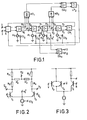
- Figure 1 shows a frequency-doubling circuit according to the invention, having a balanced input I, I to which there are connected in cascade: a subtracting stage S for direct current negative feedback still further to be described, a controllable input stage A 0 having a control input CI 0 , balanced signal outputs V o , V 0 and a level output first and second full-wave rectifier circuits A 1 and A 2 , respectively having respective control inputs CI 1 and CI 2 , rectifier outputs V 0 2 and V 1 2 and balanced signal outputs V 1 , V 1 and V 2 , V 2 , this second full-wave rectifier circuit A 2 having a level output R 2 .
- variable-gain amplifier arrangement A 3 having a control input CI 3 and balanced signal outputs V 3 , V 3 which for said direct current negative feedback are fed back to an inverting input of. the subtracting stage S via a low-pass filter LP 1 .
- the rectifier outputs V 2 and V 1 2 are coupled to a differential input of a difference stage DA 1 , which supplies the desired second harmonic of the fundamental wave in the balanced form fran a balanced output O, O of the frequency-doubling circuit.
- Figure 2 shows the circuit arrangement of the second full-wave rectifier circuit A 2 , whose terminals have been given the same reference numerals as those in Figure 1.
- This circuit comprises a balanced pair of transistors T 1 , T 2 in a long-tail configuration with a controllable current source incorporated in the common emitter lead and a balanced resistance bridge R x -R z in the col- lectar leads.
- the controllable current source has the control input CI 2 and the common emitter lead is coupled to the rectifier output V 1 2 .
- the signal input V 1 , V 1 is constituted by the base inputs of T 1 and T 2 and the signal output V 2 , V 2 by the collector outputs.
- the resistance bridge R x -R z comprises two collector resistors (R , R ) each comprising two serially connected resistor parts R and R , the common connection x of the resistor parts of the one collector resistor being connected to the common connection of the resistor parts of the other collector resistor through bridge resistor 2R , which is divided into two equal portions.
- the centre tap of the bridge resistor 2R z is coupled to a level output R 2 and supplies a d.c.
- the circuit shown acts from input V 1 , V 1 to output V2' V 2 as a variable-gain amplifier arrangement.
- the signal gain depends in a manner known per se on the magnitude of the emitter tail current which is controllable by means of a control signal via the control input CI 2 of the controllable current source in the common emitter lead.
- the collector resistors R x , R of the pair of transistors T 1 , T 2 form together with intrinsic parasitic collector capacitances (not shown) and the input capacitance of the subsequent circuit coupled to the collectors, a RC-network which is predominantly of the first order.
- the frequency of the fundamental wave is much higher than the cross-over frequency of this RC-network, it is subjected to a predominantly 90 0- phase shift. Consequently the circuit shown also functions as a 90 0- phase shifter.
- the circuit shown functions from the input V 1 , V 1 to the common emitter lead also as a full-wave rectifier circuit. It is obvious that then the gain from the input V 1 , V 1 to the signal output V 2 , V 2 is directly associated with and, at a variation of the emitter tail current, varies in the same direction as the gain from the input V 1 , V 1 to the conmon emitter lead which is coupled to rectifier output V 1 2 ,
- the signal at the common emitter lead of the pair of transistors is not utilized and this emitter lead is not coupled to an output terminal.
- the bridge resistor 2R and a level output are not present and the collector resistors are not divided, which also applies to the circuit of the variable gain amplifier arrangement A 3 .
- the common emitter lead is not coupled to an output terminal.
- the full-wave rectification in A 1 and A 2 , the 90°-phase shift at the output V 1 , V 1 of A 1 and forming the difference in the differential stage DA 1 are important for forming the second harnonic of the fundamental wave.
- the full-wave rectified fundamental waves at V 2 and V 1 2 must also have equal amplitudes, that is to say the gain of A 1 must be equal to unity at the frequency of the fundamental wave. Because of process inaccuracies and variable ambient factors it is advantageous to stabilize the gain of A 1 adaptively to unity. In the embodiment shown this is accomplished by adjusting the gain of the fundamental wave in each of the circuits A 0 -A 3 to one by means of negative feedback of the amplitude difference between the fundamental wave at the output V 0 , V 0 , of A 0 and the fundamental wave at V 2 , V 2 of A 2 to the respective control inputs CI 0 -CI 3 of said circuits A 0 -A 3 .
- the differential stage DA 2 applies the desired control signal to the control inputs CI 1 -CI 3 of the circuits A 0 -A 3 via a low-pass filter LP 2 , which control signal causes the gain of A 0 -A 3 to decrease at a positive amplitude difference, that is to say when the amplitude of the fundamental wave at the output V 2 , V 2 of A 2 exceeds the amplitude at the output V 0 , V 0 of A 0 , and to increase in the opposite case.
- each of these amplitude detectors comprises a differential amplifier of a structure as shown in Figure 3.
- This structure comprises a parallel pair of transistors T 3 , T 4 which are interconnected by means of their collectors and their emitters and effect full-wave rectification of the balanced fundamental wave applied to the bases V, V.
- the direct current component of the fundamental wave thus rectified at the common emitter is a measure of the fundamental amplitude so that this parallel pair of transistors T 3 , T 4 acts as an amplitude detector.
- the parallel pair of transistors T 3 , T 4 is connected to a supply voltage via the common collector lead and forms together with an emitter-coupled transistor T 5 a differential amplifier having the bases V , V of T 3 , T 4 as one input and the base of T5 as the other input. Then, the commn emitter lead is connected to ground via a constant emitter current source and the output of this differential amplifier is constituted by the collector of T 5 , which is connected to the supply voltage via a load resistor.
- a base biasing voltage which at a certain reference amplitude (for example 100 mV ) of the balanced fundamental wave at the bases of T 3 , T 4 keeps the differential amplitude in the balanced condition, is applied to the base of the transistor T 5 .
- said base biasing voltage can be adjusted to the desired value by a chosen ratio between R x and R y in the circuit of Figure 2. If the amplitude of the balanced fundamental wave at the bases of T 3 p T 4 decreases, then the collector output voltage of T 5 will deviate in the negative sense fran its balance setting value and vice versa. The variation of the collector output voltage of T 5 around this balanced setting value is rather linear and is not disturbed by a signal unbalance or DC-offset in the preceding circuits.
Landscapes
- Amplifiers (AREA)
- Electrotherapy Devices (AREA)
- Lock And Its Accessories (AREA)
- Stabilization Of Oscillater, Synchronisation, Frequency Synthesizers (AREA)
Applications Claiming Priority (2)
| Application Number | Priority Date | Filing Date | Title |
|---|---|---|---|
| NL8303855 | 1983-11-10 | ||
| NL8303855A NL8303855A (nl) | 1983-11-10 | 1983-11-10 | Frequentieverdubbelschakeling. |
Publications (2)
| Publication Number | Publication Date |
|---|---|
| EP0142884A1 true EP0142884A1 (de) | 1985-05-29 |
| EP0142884B1 EP0142884B1 (de) | 1988-09-07 |
Family
ID=19842690
Family Applications (1)
| Application Number | Title | Priority Date | Filing Date |
|---|---|---|---|
| EP84201593A Expired EP0142884B1 (de) | 1983-11-10 | 1984-11-05 | Frequenzverdopplungsschaltung |
Country Status (6)
| Country | Link |
|---|---|
| US (1) | US4639679A (de) |
| EP (1) | EP0142884B1 (de) |
| JP (1) | JPS60117804A (de) |
| DE (1) | DE3473977D1 (de) |
| HK (1) | HK82691A (de) |
| NL (1) | NL8303855A (de) |
Cited By (3)
| Publication number | Priority date | Publication date | Assignee | Title |
|---|---|---|---|---|
| EP0404598A3 (de) * | 1989-06-23 | 1991-09-11 | Rank Taylor Hobson Limited | Interpolator |
| DE102008048061B4 (de) * | 2007-09-21 | 2014-10-16 | Samsung Electro-Mechanics Co., Ltd. | LC-Quadratur-Oszillator mit Phasen- und Amplitudenfehlanpassungskompensator und zugehöriges Fehlanpassungskompensationsverfahren |
| CN115001458A (zh) * | 2022-07-19 | 2022-09-02 | 新风光电子科技股份有限公司 | 一种正交光电编码器脉冲信号任意次倍频控制方法 |
Families Citing this family (9)
| Publication number | Priority date | Publication date | Assignee | Title |
|---|---|---|---|---|
| DE4018616C2 (de) * | 1989-06-09 | 1996-07-18 | Telefunken Microelectron | Schaltungsanordnung zur Frequenzverdopplung |
| DE4227166C1 (de) * | 1992-08-17 | 1993-04-29 | Siemens Ag, 8000 Muenchen, De | |
| US5365181A (en) * | 1993-03-15 | 1994-11-15 | Texas Instruments Incorporated | Frequency doubler having adaptive biasing |
| US5434522A (en) * | 1993-09-08 | 1995-07-18 | Mpr Teltech Ltd. | Frequency doubler circuit having a diode quad with a grounded port |
| US7239854B2 (en) * | 2002-03-15 | 2007-07-03 | Infineon Technologies Ag | Frequency-doubling circuit arrangement, and mobile radio having that circuit arrangement |
| US7512188B1 (en) * | 2003-04-10 | 2009-03-31 | Xilinx, Inc. | Phase shift keying signaling for integrated circuits |
| US6882191B2 (en) * | 2003-06-23 | 2005-04-19 | M2 Networks, Inc. | Rectifier type frequency doubler with harmonic cancellation |
| JP2006191352A (ja) * | 2005-01-06 | 2006-07-20 | Mitsubishi Electric Corp | 電流再利用型周波数逓倍器 |
| JP2016058773A (ja) * | 2014-09-05 | 2016-04-21 | ルネサスエレクトロニクス株式会社 | 半導体装置及び無線通信装置 |
Citations (2)
| Publication number | Priority date | Publication date | Assignee | Title |
|---|---|---|---|---|
| US2440465A (en) * | 1944-09-04 | 1948-04-27 | Farnsworth Res Corp | Rectifier circuit frequency multiplier |
| US3710146A (en) * | 1970-07-09 | 1973-01-09 | Sony Corp | Frequency doubler circuit |
Family Cites Families (1)
| Publication number | Priority date | Publication date | Assignee | Title |
|---|---|---|---|---|
| US3764927A (en) * | 1971-12-07 | 1973-10-09 | Gen Datacomm Ind Inc | Wide band frequency discriminator |
-
1983
- 1983-11-10 NL NL8303855A patent/NL8303855A/nl not_active Application Discontinuation
-
1984
- 1984-11-05 DE DE8484201593T patent/DE3473977D1/de not_active Expired
- 1984-11-05 EP EP84201593A patent/EP0142884B1/de not_active Expired
- 1984-11-10 JP JP59236009A patent/JPS60117804A/ja active Pending
- 1984-11-13 US US06/671,151 patent/US4639679A/en not_active Expired - Fee Related
-
1991
- 1991-10-24 HK HK826/91A patent/HK82691A/xx unknown
Patent Citations (2)
| Publication number | Priority date | Publication date | Assignee | Title |
|---|---|---|---|---|
| US2440465A (en) * | 1944-09-04 | 1948-04-27 | Farnsworth Res Corp | Rectifier circuit frequency multiplier |
| US3710146A (en) * | 1970-07-09 | 1973-01-09 | Sony Corp | Frequency doubler circuit |
Cited By (4)
| Publication number | Priority date | Publication date | Assignee | Title |
|---|---|---|---|---|
| EP0404598A3 (de) * | 1989-06-23 | 1991-09-11 | Rank Taylor Hobson Limited | Interpolator |
| DE102008048061B4 (de) * | 2007-09-21 | 2014-10-16 | Samsung Electro-Mechanics Co., Ltd. | LC-Quadratur-Oszillator mit Phasen- und Amplitudenfehlanpassungskompensator und zugehöriges Fehlanpassungskompensationsverfahren |
| CN115001458A (zh) * | 2022-07-19 | 2022-09-02 | 新风光电子科技股份有限公司 | 一种正交光电编码器脉冲信号任意次倍频控制方法 |
| CN115001458B (zh) * | 2022-07-19 | 2022-11-11 | 新风光电子科技股份有限公司 | 一种正交光电编码器脉冲信号任意次倍频控制方法 |
Also Published As
| Publication number | Publication date |
|---|---|
| US4639679A (en) | 1987-01-27 |
| HK82691A (en) | 1991-11-01 |
| DE3473977D1 (en) | 1988-10-13 |
| EP0142884B1 (de) | 1988-09-07 |
| NL8303855A (nl) | 1985-06-03 |
| JPS60117804A (ja) | 1985-06-25 |
Similar Documents
| Publication | Publication Date | Title |
|---|---|---|
| US5489873A (en) | Active low-pass filter | |
| EP0142884B1 (de) | Frequenzverdopplungsschaltung | |
| EP0393717A2 (de) | Aktive Filterschaltung | |
| KR20010098905A (ko) | 주파수 체배 회로 및 반도체 집적 회로 | |
| US5650749A (en) | FM demodulator using injection locked oscillator having tuning feedback and linearizing feedback | |
| US5483195A (en) | Second generation low noise microwave voltage controlled oscillator | |
| US6356131B1 (en) | 90-degree phase shifter | |
| GB2053608A (en) | Variable frequency oscillator | |
| US5479137A (en) | Controlled oscillator, as for synchyronous video detector | |
| EP0336206B1 (de) | Schaltungsanordnung zur Kompensierung der thermischen Nacheilung eines Phasendetektors | |
| US4253118A (en) | Synchronous detection system | |
| EP1236285B1 (de) | Empfängerschaltung | |
| EP0365091A2 (de) | Filterschaltungsanordnung | |
| US4536717A (en) | Compensated inverting/noninverting differential amplifier | |
| JPS63500839A (ja) | 平衡可変リアクタンス発生回路及びその発生方法 | |
| US4745370A (en) | Adjustable phase shift circuit | |
| US4283693A (en) | Amplitude tilt compensating apparatus | |
| US5115212A (en) | Integrable variable-frequency oscillator circuit | |
| EP0453035B1 (de) | Regelbare Oszillatorschaltung | |
| US4675616A (en) | Second order all pass network | |
| US4510452A (en) | Circuit having square-law transfer characteristic | |
| JPS6230521B2 (de) | ||
| US4616186A (en) | FM quadrature demodulator with distortion compensation | |
| US4306306A (en) | Amplitude tilt and notch compensation apparatus | |
| JP2932502B2 (ja) | 差動増幅回路 |
Legal Events
| Date | Code | Title | Description |
|---|---|---|---|
| PUAI | Public reference made under article 153(3) epc to a published international application that has entered the european phase |
Free format text: ORIGINAL CODE: 0009012 |
|
| AK | Designated contracting states |
Designated state(s): DE FR GB IT |
|
| 17P | Request for examination filed |
Effective date: 19851128 |
|
| 17Q | First examination report despatched |
Effective date: 19870331 |
|
| GRAA | (expected) grant |
Free format text: ORIGINAL CODE: 0009210 |
|
| AK | Designated contracting states |
Kind code of ref document: B1 Designated state(s): DE FR GB IT |
|
| REF | Corresponds to: |
Ref document number: 3473977 Country of ref document: DE Date of ref document: 19881013 |
|
| ITF | It: translation for a ep patent filed | ||
| ET | Fr: translation filed | ||
| PLBE | No opposition filed within time limit |
Free format text: ORIGINAL CODE: 0009261 |
|
| STAA | Information on the status of an ep patent application or granted ep patent |
Free format text: STATUS: NO OPPOSITION FILED WITHIN TIME LIMIT |
|
| 26N | No opposition filed | ||
| PGFP | Annual fee paid to national office [announced via postgrant information from national office to epo] |
Ref country code: DE Payment date: 19900125 Year of fee payment: 6 |
|
| PGFP | Annual fee paid to national office [announced via postgrant information from national office to epo] |
Ref country code: GB Payment date: 19901031 Year of fee payment: 7 |
|
| PGFP | Annual fee paid to national office [announced via postgrant information from national office to epo] |
Ref country code: FR Payment date: 19901123 Year of fee payment: 7 |
|
| ITTA | It: last paid annual fee | ||
| PG25 | Lapsed in a contracting state [announced via postgrant information from national office to epo] |
Ref country code: DE Effective date: 19910801 |
|
| PG25 | Lapsed in a contracting state [announced via postgrant information from national office to epo] |
Ref country code: GB Effective date: 19911105 |
|
| GBPC | Gb: european patent ceased through non-payment of renewal fee | ||
| PG25 | Lapsed in a contracting state [announced via postgrant information from national office to epo] |
Ref country code: FR Effective date: 19920731 |
|
| REG | Reference to a national code |
Ref country code: FR Ref legal event code: ST |