EP0142063A1 - Lighting apparatus for an electric discharge lamp - Google Patents
Lighting apparatus for an electric discharge lamp Download PDFInfo
- Publication number
- EP0142063A1 EP0142063A1 EP84112573A EP84112573A EP0142063A1 EP 0142063 A1 EP0142063 A1 EP 0142063A1 EP 84112573 A EP84112573 A EP 84112573A EP 84112573 A EP84112573 A EP 84112573A EP 0142063 A1 EP0142063 A1 EP 0142063A1
- Authority
- EP
- European Patent Office
- Prior art keywords
- circuit
- power supply
- electric power
- lighting
- discharge lamp
- Prior art date
- Legal status (The legal status is an assumption and is not a legal conclusion. Google has not performed a legal analysis and makes no representation as to the accuracy of the status listed.)
- Granted
Links
- 239000003990 capacitor Substances 0.000 claims abstract description 72
- 230000000087 stabilizing effect Effects 0.000 claims abstract description 4
- 230000010355 oscillation Effects 0.000 claims description 17
- 238000004804 winding Methods 0.000 claims description 16
- 238000010586 diagram Methods 0.000 description 9
- 230000007423 decrease Effects 0.000 description 5
- 230000000694 effects Effects 0.000 description 4
- 238000000034 method Methods 0.000 description 4
- 239000004065 semiconductor Substances 0.000 description 3
- 230000002950 deficient Effects 0.000 description 2
- 230000005856 abnormality Effects 0.000 description 1
- 230000015556 catabolic process Effects 0.000 description 1
- 238000007599 discharging Methods 0.000 description 1
- 230000001788 irregular Effects 0.000 description 1
- 230000003252 repetitive effect Effects 0.000 description 1
- 230000000630 rising effect Effects 0.000 description 1
Images



Classifications
-
- H—ELECTRICITY
- H05—ELECTRIC TECHNIQUES NOT OTHERWISE PROVIDED FOR
- H05B—ELECTRIC HEATING; ELECTRIC LIGHT SOURCES NOT OTHERWISE PROVIDED FOR; CIRCUIT ARRANGEMENTS FOR ELECTRIC LIGHT SOURCES, IN GENERAL
- H05B41/00—Circuit arrangements or apparatus for igniting or operating discharge lamps
- H05B41/14—Circuit arrangements
- H05B41/26—Circuit arrangements in which the lamp is fed by power derived from DC by means of a converter, e.g. by high-voltage DC
- H05B41/28—Circuit arrangements in which the lamp is fed by power derived from DC by means of a converter, e.g. by high-voltage DC using static converters
- H05B41/295—Circuit arrangements in which the lamp is fed by power derived from DC by means of a converter, e.g. by high-voltage DC using static converters with semiconductor devices and specially adapted for lamps with preheating electrodes, e.g. for fluorescent lamps
- H05B41/298—Arrangements for protecting lamps or circuits against abnormal operating conditions
- H05B41/2981—Arrangements for protecting lamps or circuits against abnormal operating conditions for protecting the circuit against abnormal operating conditions
-
- Y—GENERAL TAGGING OF NEW TECHNOLOGICAL DEVELOPMENTS; GENERAL TAGGING OF CROSS-SECTIONAL TECHNOLOGIES SPANNING OVER SEVERAL SECTIONS OF THE IPC; TECHNICAL SUBJECTS COVERED BY FORMER USPC CROSS-REFERENCE ART COLLECTIONS [XRACs] AND DIGESTS
- Y10—TECHNICAL SUBJECTS COVERED BY FORMER USPC
- Y10S—TECHNICAL SUBJECTS COVERED BY FORMER USPC CROSS-REFERENCE ART COLLECTIONS [XRACs] AND DIGESTS
- Y10S315/00—Electric lamp and discharge devices: systems
- Y10S315/07—Starting and control circuits for gas discharge lamp using transistors
Definitions
- the present invention relates to a lighting apparatus for an electric discharge lamp which lights up an electric discharge lamp and, more particularly, to a circuit arrangement of a lighting apparatus for an electric discharge lamp which is suitable to drive with a high efficiency.
- the power supply to this oscillating section is generally obtained by a method whereby the AC power is dropped to the voltage level that is needed for the oscillating section by a stepdown transformer and then it is rectified by a full wave rectifier.
- the stepdown transformer and full wave rectifier are necessary to obtain the power for the oscillating section, so that there is a drawback such that the circuit scale is large and expensive.
- this method has drawbacks such that the resistance value becomes large when the voltage is high and that the electric power which is consumed by the resistor increases.
- the lighting electric power is continuously supplied irrespective of the lighting state of the electric discharge lamp since the oscillating section continuously operates during the time interval when the power supply is turned on.
- the continuation of operation of such an inverter apparatus causes the light electric power generated to be consumed in vain and also causes a high voltage to be developed while the discharge lamp is lit off.
- the conventional lighting apparatuses still have various problems left that have to be solved.
- Another object of the invention is to provide a lighting apparatus for an electric discharge lamp which can immediately stop the operation when the discharge lamp is removed or when abnormality such as disconnection of a preheating electrode or the like occurs in the lighting circuit.
- the present invention relates to a lighting apparatus for an electric discharge lamp comprising:
- a reference numeral 3 denotes a full wave rectifier connected to an AC power supply 1 for commercial use, and 40 is a capacitor connected between the output terminals of the full wave rectifier 3 and consitutes a DC power supply 80.
- a numeral 11 is an output transformer whose center tap is coupled to one end of the capacitor 40. One end of the winding of the output transformer 11 is connected to the collector of a transistor 20. The other end of the winding of the output transformer 11 is connected to one preheating electrode 30a of an electric discharge lamp 30 such as a fluorescent lamp through a ballast capacitor 41 as a ballast element for light-up.
- the preheating electrode 30a is connected to the other preheating electrode 30b through a preheating capacitor 42 as a preheating ballast element.
- the output terminal of the full wave rectifier 3 is connected to one input terminal of a full wave rectifier 4.
- the preheating electrode 30b is further connected to the other input terminal of the full wave rectifier 4.
- a numeral 43 is a capacitor connected between the output terminals of the full wave rectifier 4, and 10 is an oscillator constituting a part of an inverter circuit 70.
- the oscillator 10 uses an output electric power of the full wave rectifier 4 as a control power source.
- the output signal of repetitive width pulses of the oscillator 10 is inputted to the base of the main oscillating transistor 20.
- the emitter of the transistor 20 is connected to the output terminal of the full wave rectifier 4.
- the operation of the lighting apparatus for an electric discharge lamp constituted in this way will be explained.
- the AC power supply 1 when the AC power supply 1 is turned on, the current rectified by the full wave rectifier 3 is charged in the capacitor 40 and is charged in the capacitor 43 through the output transformer 11, ballast capacitor 41, preheating electrode 30a of the discharge lamp 30, preheating capacitor 42, the other preheating electrode 30b of the discharge lamp 30, and full wave rectifier 4.
- the oscillator 10 starts oscillating, thereby making the transistor 20 operative.
- the current is supplied to the output transformer 11.
- the current flows from the output transformer 11 through the ballast capacitor 41, preheating electrode 30a of the discharge lamp 30, preheating capacitor 42, preheating electrode 30b of the discharge lamp 30, full wave rectifier 4, and capacitor 43.
- the preheating electrodes 30a and 30b of the discharge lamp 30 are preheated due to this current flow, and at the same time the control electric power which is enough to allow the oscillator 10 to operate stably is supplied to the oscillator 10. Further, when the preheating electrodes 30a and 30b of the discharge lamp 30 are preheated and the voltage developed across the preheating capacitor 42 is simultaneously applied to both ends of the discharge lamp 30, so that the discharge lamp 30 is lit on after the preheating electrodes 30a and 30b were sufficiently preheated. When the discharge lamp 30 has been lit on, the DC electric power is supplied to the oscillator 10 through the output transformer 11, ballast capacitor 41, discharge lamp 30, and full wave rectifier 4; therefore, the stable oscillation can be continued.
- the electrical circuit section can be made small and there is also an effect such that the electric power loss can be made small since the control electric power can be supplied to the oscillator 10 without passing through a resistor.
- the control electric power is all supplied through the discharge lamp 30 to the oscillator 10; consequently, when the discharge lamp 30 is removed from the circuit, the supply of the control power to the oscillator 10 completely stops, thereby enabling the oscillation to be certainly stopped.
- the full wave rectifier 4 in the embodiment of Fig. 1 serves to rectify the current which is supplied to the oscillator 10 through the discharge lamp 30.
- This rectifier 4 may be substituted by a half wave rectifier consisting of diodes 31 and 32 which are connected in series in the same direction as shown in Fig. 2.
- a Zener diode 33 when a Zener diode 33 is connected in parallel to the capacitor 43 as shown in Fig. 2, the voltage across the capacitor 43 becomes stable at the voltage level that is determined by the Zener voltage of the Zener diode 33, so that it is possible to supply to the transistor 20 the base signal which repeats at a constant period irrespective of the variation in power supply voltage.
- the output transformer is constituted by the autotransformer having no secondary winding.
- the control electric power may be supplied to the oscillator 10 through the capacitor 44 when the AC power supply 1 is turned on and after the oscillation started, the control power may be supplied through the output transformer 11, ballast capacitor 41, discharge lamp 30, preheating capacitor 42, and a feedback transformer 13 and then through a full wave rectifier 5.
- Fig. 6 shows a lighting apparatus for an electric discharge lamp whereby an emitter-coupled stable multivibrator using a transistor is used in the oscillator 10 and a positive characteristic thermistor 60 is connected in series to the preheating capacitor 42.
- an inverter circuit 77 started oscillating due to the turn-on of the AC power supply 1
- the discharge lamp 30 does not change to the lighting state due to some reason but holds the preheating state.
- the resistance value of the positive characteristic thermistor 60 increases due to the self-exothermic since the preheating current flows through the termistor 60.
- the voltage across the capacitor 43 which is the power supply voltage of the oscillator 10 decreases with an increase in that resistance value.
- the voltage across the capacitor 43 decreases and therefore the voltage across a resistor 52 becomes a voltage less than the base-emitter voltage at which the transistor 22 can operate, the transistor 22 cannot be driven; consequently, the oscillator 10 stops oscillating and the inverter circuit 77 stops. In this way, if the circuit which stops the oscillation in association with the reduction of the power supply voltage is used in the oscillator 10, the oscillating operation of the oscillator 10 can be stopped by reducing the power supply current without cutting the power supply current to the oscillator 10, thereby enabling the operation of the discharge lamp inverter to be stopped.
- the operation of the inverter for the discharge lamp can be stopped by removing the discharge lamp from the circuit, so that a high voltage is not generated in the discharge lamp socket and the safety is assured.
- the circuit is not made operative, so that the electric power is not consumed in vain.
- the circuit does not operate in the loadless state whereby an excessive burden is imparted to the circuit element, there is also another effect such that the burden to the circuit element can be reduced.
- numerals 81, 82 and 83 denote a resistor, a capacitor and a reactor which together constitute a noise filter; 84 is a power switch; and 85 is a resistor connected in parallel to the capacitor 40.
- the DC power supply 80 is constituted by rectifying these AC power supply 1 for commercial use.
- a numeral 110 denotes a semiconductor integrated circuit (e.g., NE555 made by Signetics, Co. Ltd., or the like) for a timer equipped with a voltage comparator, SR flip flop circuit, etc. therein.
- the oscillator is,constituted using the semiconductor integrated circuit 110 as a principal component.
- Numerals 31 and 32 are the diodes to feed back the control electric power to the oscillating element 110 consisting of the semiconductor integrated circuit.
- a low voltage is supplied to the diodes 3l and 32 through the discharge lamp 30.
- Numerals 33 and 43 are a Zener diode and a capacitor to stabilize the electric power which is supplied to the oscillating element 110 and these elements constitute a control power supply circuit 90 of the oscillating circuit.
- a numeral 100 is an oscillation time constant circuit to determine the oscillating condition (operational condition) of the oscillating element 110 and comprises the following elements. Namely, one end of a capacitor 101 is connected to a threshold terminal E of the oscillating element 110. Resistors 102 and 105 are connected between the threshold terminal E and a discharge terminal F of the oscillating element 110. Also, a diode 103 is connected in series to the resistor 102, thereby making the conditions for charge and discharge into and from the capacitor 101 different.
- a resistor 104 is connected between the discharge terminal F and the operating power supply.
- a power terminal A of the oscillating element 110 is connected to the operating power supply, while an earth terminal D is connected to a grouding electrode side of the DC power supply 80, respectively.
- a numeral 120 is a temperature protecting circuit to detect the overheat of the transistor 20 and stop the operation of the oscillating element 110. Namely, the temperature protecting circuit 120 utilizes a reset terminal C of the oscillating element 110 and a-series circuit consisting of a resistor 123, a Zener diode 122 and a resistor 121 is connected between the power terminal A and the grounding terminal D of the oscillating element 110.
- the node of the resistor 123 and Zener diode 122 is connected to the grounding terminal D through a thermistor 124.
- the node of the Zener diode 122 and resistor 121 is connected to the reset terminal C of the oscillating element 110.
- An output terminal B of the oscillating element 110 is connected to the base of the transistor 20 through a capacitor 132 for improvement of the waveform and through a resistor 131.
- a resistor 133 is for the base bias of the transistor 20.
- Numerals 201 and 202 are shielding wires which constitute the current feeding line for supplying a high frequency AC electric power of the lighting circuit for the electric discharge lamp 30. The shields of these shielding wires are grounded through an earth capacitor 203.
- the output transformer 11 consisting of the autotransformer and the transistor 20 as the switching element constitute electric power supply means 130 for converting the DC electric power to the high frequency AC electric power.
- one end of the ballast capacitor 41 for light-up is connected to one end 30a 1 of the preheating electrode 30a of the discharge lamp 30 having a pair of preheating elements; the ballast capacitor 42 for preheating is connected between the other end 30a 2 of the preheating electrode 30a and one end 30b 1 of the other preheating electrode 30b; further, the other end 30b 2 of the preheating electrode 30b is connected to the negative electrode side of the DC power supply 80 through the control power supply circuit 90, respectively; and thereby constituting the lighting circuit for the discharge lamp 30.
- control power supply circuit 90 as the converter for converting the lighting current which flows through the lighting circuit to the voltage signal and to regard the oscillating element 110 as the power control circuit which receives the voltage signal from the converter and controls the electric power supply means 130.
- (a) denotes an output signal of the oscillator and (b) and (c) respectively represent a switching current Ic and a resonance voltage Vce at the lighting and preheating times.
- the oscillator starts the oscillating operation and holds its output signal at a Hi level during the predetermined interval A.
- the switching current Ic flows into the transistor 20 through the output transformer 11.
- the output signal of the oscillator becomes a Lo level (this interval is shown by the interval B) after the elapse of the interval A, the switching current Ic of the transistor 20 is shut off, so that this causes the series resonance due to the output transformer 11 and time constant of each ballast element 41 (or 42) connected in series thereto.
- the series resonance that is determined by the output transformer 11 and time constant due to the ballast capacitor 41 occurs, so that the lighting current in association with this series resonance flows through the output transformer 11, ballast capacitor 41 and discharge lamp 30.
- the series resonance that is determined by the output transformer 11 and time constant due to the ballast capacitor 41 and preheating capacitor 42 occurs, so that the preheating current in association with this series resonance flows through the output transformer 11, ballast capacitor 41, preheating electrode 30a of the discharge lamp 30, preheating capacitor 42, and preheating electrode 30b.
- the series resonance occurs on the basis of the output signal of the oscillator and the necessary preheating current and lighting current are fed to the electric discharge lamp.
- the preheating capacitor 42 since the preheating capacitor 42 is connected in series to the ballast capacitor 41 at the preheating time, the resonance frequency thereof becomes higher than that during the lighting state; however, the oscillating period of the oscillator is set to be constant. Thus, even if the resonance frequency increases at the preheating time, the capacity of the preheating capacitor 42 is selected such that the conduction timing of the switching element 20 and the rising timing of the resonance voltage do not overlap. Practically speaking, the circuit constant is selected such that the switching element 20 is made conductive immediately before the second positive leading edge of the resonance voltage at the preheating time. This is because, as shown in Fig. 8(d), when the swtiching element 20 is rendered conductive at the leading time of the resonance voltage, the increasing rate of current of the switching element becomes large, causing a risk of thermal breakdown of the switching element 20.
- the resistance value of the thermistor 124 when the temperature of the transistor 20 is low, the resistance value of the thermistor 124 is high and the voltage across the ther- . mistor 124 exceeds the Zener voltage of the Zener diode 122, so that the current flows through the Zener diode 122 and the voltage drop of the resistor 121 is insufficient. Therefore, the reset siganl is not supplied to the oscillating element 110 and the oscillating element 110 continues the oscillating operation.
- the resistance value of the thermistor 124 decreases and the potential across the thermistor 124 decreases, so that no current flows through the Zener diode 122.
- the voltage drop of the resistor 121 i.e., the potential at the reset terminal C becomes low and the reset signal is supplied to the reset terminal C, causing the oscillating element l10 to stop the oscillating operation.
- Fig. 9 shows an example whereby the increase in temperature of the transistor 20 is detected by the thermistor 124 and a thyristor 300 is made conductive, thereby short-circuiting the control power supply of the oscillating element 110 and stopping the oscillating operation of the oscillating element 110.
- Fig. 10 shows an example whereby the thermistor 124 is built in the oscillation time constant circuit and when the increase in temperature of the transistor 20 is detected, the oscillator is controlled such that the ON-interval of the transistor 20 is shortened.
- Fig. 10 shows an example whereby the increase in temperature of the transistor 20 is detected by the thermistor 124 is built in the oscillation time constant circuit and when the increase in temperature of the transistor 20 is detected, the oscillator is controlled such that the ON-interval of the transistor 20 is shortened.
- the protecting operation can be also similarly performed when the protecting circuit is constituted in the manner such that the reset terminal C of the oscillating element 110 is short-circuited onto the negative polarity side of the DC power supply when the increase in temperature of the transistor 20 is detected by the thermistor 124.
Landscapes
- Circuit Arrangements For Discharge Lamps (AREA)
Abstract
Description
- The present invention relates to a lighting apparatus for an electric discharge lamp which lights up an electric discharge lamp and, more particularly, to a circuit arrangement of a lighting apparatus for an electric discharge lamp which is suitable to drive with a high efficiency.
- In a lighting apparatus for an electric discharge lamp having a separately excited inverter apparatus which is equipped with an oscillating section and converts a DC electric power to an AC electric power by the output of this oscillating section, the power supply to this oscillating section is generally obtained by a method whereby the AC power is dropped to the voltage level that is needed for the oscillating section by a stepdown transformer and then it is rectified by a full wave rectifier. However, in this method, the stepdown transformer and full wave rectifier are necessary to obtain the power for the oscillating section, so that there is a drawback such that the circuit scale is large and expensive. There is another method whereby such a power is directly derived through a resistor after the AC power was rectified. However, this method has drawbacks such that the resistance value becomes large when the voltage is high and that the electric power which is consumed by the resistor increases.
- In addition, in a separately excited inverter apparatus, the lighting electric power is continuously supplied irrespective of the lighting state of the electric discharge lamp since the oscillating section continuously operates during the time interval when the power supply is turned on. The continuation of operation of such an inverter apparatus causes the light electric power generated to be consumed in vain and also causes a high voltage to be developed while the discharge lamp is lit off.
- On the other hand, as a lighting apparatus for an electric discharge lamp having a self-excited inverter apparatus equipped with a base feedback winding, there have been proposed an apparatus in which no oscillation occurs even when the power supply is turned on in the case where the electric discharge lamp is removed, and an apparatus which stops the oscillation in the case where the preheating electrode is disconnected. These apparatuses are disclosed in Japanese Utility Model Publication Laid-open No. 15978/73 and Japanese Patent Publication Laid-open No. 3313/79, etc. However, there is a case where the oscillation has once started, the oscillation does not stop even if the discharge lamp was removed after the light-up or even if the discharge lamp was lit off due to the disconnection of the preheating electrode. Also, although it is possible to detect the defective assembly and disconnection of the preheating electrode of one discharge lamp, the defective assembly and disconnection of the other preheating electrode cannot be detected, so that the service life of the lamp will have been shortened and the unstable operation will have been continued, and the like. Therefore, the conventional lighting apparatuses still have various problems left that have to be solved.
- It is an object of the present invention to obtain the necessary control electric power by supplying the electric power through an electric discharge lamp to an oscillating section of a separately excited inverter circuit without using a stepdown transformer or a resistive element for voltage drop, thereby to reducing the loss of electric power by the circuit itself of a lighting apparatus for an electric discharge lamp and to realize the miniaturization and high efficiency of the lighting apparatus for an electric discharge lamp.
- Another object of the invention is to provide a lighting apparatus for an electric discharge lamp which can immediately stop the operation when the discharge lamp is removed or when abnormality such as disconnection of a preheating electrode or the like occurs in the lighting circuit.
- The present invention relates to a lighting apparatus for an electric discharge lamp comprising:
- a lighting ballast element, connected in series to an electric discharge lamp, for stabilizing a lighting current to the discharge lamp; a preheating ballast element, connected in parallel to the discharge lamp, for supplying a preheating electric power to the discharge lamp; electric power supply means for supplying an electric power to the lighting ballast element; a control power supply circuit for obtaining a control electric power through the lighting ballast element and discharge lamp or the preheating ballast element connected in parallel to the discharge lamp without, in particular, adding a stepdown transformer or a resistive element for voltage drop; and an oscillator which receives the control electric power from the control power supply circuit and controls the electric power supply means, thereby making the electric power loss small and realizing the miniaturization.
- The present invention will be apparent from the following detailed description taken in conjunction with the accompanying drawings, in which:
- Fig. 1 is a circuit diagram showing a fundamental embodiment of the present invention, in which a control power supply circuit is constituted as a full wave rectifier;
- Fig. 2 is a circuit diagram also showing a fundamental embodiment of the invention, in which the control power supply circuit is constituted as a half wave rectifier;
- Fig. 3 is also an improved circuit diagram of the embodiment;
- Fig. 4 shows an example of a circuit using two transistors which are alternately turned on and off;
- Fig. 5 shows an example of a circuit in the case where an output transformer of the insulating type is used;
- Fig. 6 shows an example of a circuit in which an oscillating circuit is constituted using an emitter-coupled stable multivibrator;
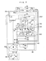
- Fig. 7 is a circuit diagram showing an example of a further practical embodiment;
- Fig. 8 shows waveform diagrams for explaining the circuit operation;
- Fig. 9 is a circuit diagram for explaining another embodiment of a temperature protecting circuit; and
- Fig. 10 is a circuit diagram showing an example of further another temperature protecting circuit.
- One embodiment of the present invention will now be described hereinbelow with reference to Fig. 1. A
reference numeral 3 denotes a full wave rectifier connected to an AC power supply 1 for commercial use, and 40 is a capacitor connected between the output terminals of thefull wave rectifier 3 and consitutes aDC power supply 80. Anumeral 11 is an output transformer whose center tap is coupled to one end of thecapacitor 40. One end of the winding of theoutput transformer 11 is connected to the collector of atransistor 20. The other end of the winding of theoutput transformer 11 is connected to one preheatingelectrode 30a of anelectric discharge lamp 30 such as a fluorescent lamp through aballast capacitor 41 as a ballast element for light-up. In addition, the preheatingelectrode 30a is connected to the other preheatingelectrode 30b through a preheatingcapacitor 42 as a preheating ballast element. The output terminal of thefull wave rectifier 3 is connected to one input terminal of a full wave rectifier 4. The preheatingelectrode 30b is further connected to the other input terminal of the full wave rectifier 4. Anumeral 43 is a capacitor connected between the output terminals of thefull wave rectifier 4, and 10 is an oscillator constituting a part of aninverter circuit 70. Theoscillator 10 uses an output electric power of the full wave rectifier 4 as a control power source. The output signal of repetitive width pulses of theoscillator 10 is inputted to the base of the main oscillatingtransistor 20. Lastly, the emitter of thetransistor 20 is connected to the output terminal of the full wave rectifier 4. - Next, the operation of the lighting apparatus for an electric discharge lamp constituted in this way will be explained. First, when the AC power supply 1 is turned on, the current rectified by the
full wave rectifier 3 is charged in thecapacitor 40 and is charged in thecapacitor 43 through theoutput transformer 11,ballast capacitor 41, preheatingelectrode 30a of thedischarge lamp 30, preheatingcapacitor 42, theother preheating electrode 30b of thedischarge lamp 30, and full wave rectifier 4. When the voltage across thecapacitor 43 increases to the operating voltage of theoscillator 10, theoscillator 10 starts oscillating, thereby making thetransistor 20 operative. As the result of the operation of thetransistor 20, the current is supplied to theoutput transformer 11. The current flows from the output transformer 11 through theballast capacitor 41, preheatingelectrode 30a of thedischarge lamp 30, preheatingcapacitor 42, preheatingelectrode 30b of thedischarge lamp 30, full wave rectifier 4, andcapacitor 43. The preheatingelectrodes discharge lamp 30 are preheated due to this current flow, and at the same time the control electric power which is enough to allow theoscillator 10 to operate stably is supplied to theoscillator 10. Further, when the preheatingelectrodes discharge lamp 30 are preheated and the voltage developed across the preheatingcapacitor 42 is simultaneously applied to both ends of thedischarge lamp 30, so that thedischarge lamp 30 is lit on after the preheatingelectrodes discharge lamp 30 has been lit on, the DC electric power is supplied to theoscillator 10 through theoutput transformer 11,ballast capacitor 41,discharge lamp 30, and full wave rectifier 4; therefore, the stable oscillation can be continued. - In this way, according to this embodiment, since there is no need to add a particular circuit for dropping the power supply voltage in order to supply the control electric power to the
oscillator 10, the electrical circuit section can be made small and there is also an effect such that the electric power loss can be made small since the control electric power can be supplied to theoscillator 10 without passing through a resistor. Further, in this embodiment, the control electric power is all supplied through thedischarge lamp 30 to theoscillator 10; consequently, when thedischarge lamp 30 is removed from the circuit, the supply of the control power to theoscillator 10 completely stops, thereby enabling the oscillation to be certainly stopped. In addition, no control power is supplied to theoscillator 10 even when the AC power source 1 is applied to the inverter circuit in the state whereby thedischarge lamp 30 is not connected to the circuit or whereby either one of the preheatingelectrodes discharge lamp 30 is disconnected. Therefore, theoscillator 10 does not oscillate and theinverter circuit 70 is held stopped. Thus, this embodiment has an effect such that the loadless state in that an excessive burden is imparted to the circuit element does not exist. - The full wave rectifier 4 in the embodiment of Fig. 1 serves to rectify the current which is supplied to the
oscillator 10 through thedischarge lamp 30. This rectifier 4 may be substituted by a half wave rectifier consisting ofdiodes diode 33 is connected in parallel to thecapacitor 43 as shown in Fig. 2, the voltage across thecapacitor 43 becomes stable at the voltage level that is determined by the Zener voltage of theZener diode 33, so that it is possible to supply to thetransistor 20 the base signal which repeats at a constant period irrespective of the variation in power supply voltage. - As shwon in Fig. 3, when a
capacitor 44 is connected between the plus terminal of thefull wave rectifier 3 and the power supply input terminal of theoscillator 10, the control electric power is supplied to theoscillator 10 through theoutput transformer 11,ballast capacitor 41,discharge lamp 30, preheatingcapacitor 42, anddiode 32 and also through thecapacitor 44 at the time of turn-on of the AC power supply 1. Thus, this makes it possible to allow the start-up of theoscillator 10 to be certainly performed. When theoscillator 10 has once started operating, the amount of power source current that is supplied through thecapacitor 44 to theoscillator 10 decreases because thefull wave rectifier 3 outputs the DC voltage and the impedance of thecapacitor 44 increases. Thus, almost of the power source current is supplied to theoscillator 10 through theoutput transformer 11,ballast capacitor 41,discharge lamp 30,preheating capacitor 42, anddiode 32. - In the case where the
discharge lamp 30 is removed from the circuit when theinverter 70 is operating in the embodiment of Fig. 1, a high voltage is developed between the collector and emitter of thetransistor 20 due to the electromagnetic energy stored in theoutput transformer 11. Therefore, a transistor having a high withstanding voltage is needed as thetransistor 20. Thus, in order to allow a transistor having a low withstanding voltage to be used as thetransistor 20, it is also possible to constitute a circuit such that anavalanche diode 34 is connected between the collector and emitter of thetransistor 20 as indicated by a broken line in Fig. 3 and the electromagnetic energy of theoutput transformer 11 is absorbed by thisavalanche diode 34. On the other hand, in place of connecting theavalanche diode 34, it is also possible to connect acapacitor 45 between the center tap of theoutput transformer 11 and thetransistor 20 as likewise indicated by the broken line, thereby to absorb the electromagnetic energy of theoutput transformer 11. - As shown in Fig. 4, with respect to the circuit in which the
transistors oscillator 10 through theoutput transformer 11,ballast capacitor 41,discharge lamp 30, preheatingcapacitor 42, anddiode 32, there will be no need to add a circuit to supply the control power tQ theoscillator 10 and the electric power loss of the circuit can be also made small. - In the foregoing embodiment, the output transformer is constituted by the autotransformer having no secondary winding. However, in the case where the insulating type output transformer is used, as shown in Fig. 5, the control electric power may be supplied to the
oscillator 10 through thecapacitor 44 when the AC power supply 1 is turned on and after the oscillation started, the control power may be supplied through theoutput transformer 11,ballast capacitor 41,discharge lamp 30, preheatingcapacitor 42, and afeedback transformer 13 and then through a full wave rectifier 5. - Next, Fig. 6 shows a lighting apparatus for an electric discharge lamp whereby an emitter-coupled stable multivibrator using a transistor is used in the
oscillator 10 and a positivecharacteristic thermistor 60 is connected in series to the preheatingcapacitor 42. In such an apparatus, it is assumed that in spite of the fact that an inverter circuit 77 started oscillating due to the turn-on of the AC power supply 1, thedischarge lamp 30 does not change to the lighting state due to some reason but holds the preheating state. Due to the continuation of the preheating state, the resistance value of the positivecharacteristic thermistor 60 increases due to the self-exothermic since the preheating current flows through thetermistor 60. The voltage across thecapacitor 43, which is the power supply voltage of theoscillator 10, decreases with an increase in that resistance value. When the voltage across thecapacitor 43 decreases and therefore the voltage across aresistor 52 becomes a voltage less than the base-emitter voltage at which thetransistor 22 can operate, thetransistor 22 cannot be driven; consequently, theoscillator 10 stops oscillating and the inverter circuit 77 stops. In this way, if the circuit which stops the oscillation in association with the reduction of the power supply voltage is used in theoscillator 10, the oscillating operation of theoscillator 10 can be stopped by reducing the power supply current without cutting the power supply current to theoscillator 10, thereby enabling the operation of the discharge lamp inverter to be stopped. - According to the above-described embodiment, there is no need to provide a circuit to drop the power supply voltage to the voltage level necessary for the oscillator in order to supply the power source to the oscillator. Also, the electric power loss that is necessary for the voltage stepdown can be made small. Therefore, there is an effect such that the miniaturization and high efficiency of the lighting apparatus for an electric discharge lamp can be realized.
- In addition, according to the foregoing embodiment, the operation of the inverter for the discharge lamp can be stopped by removing the discharge lamp from the circuit, so that a high voltage is not generated in the discharge lamp socket and the safety is assured. When the discharge lamp is not connected to the circuit or when the preheating electrode of the discharge lamp is disconnected, the circuit is not made operative, so that the electric power is not consumed in vain. Further, since the circuit does not operate in the loadless state whereby an excessive burden is imparted to the circuit element, there is also another effect such that the burden to the circuit element can be reduced.
- Next, a further practical embodiment shown in Fig. 7 will be explained, in which the same parts and components as those shown in the foregoing embodiment are designated by the same reference numerals and they perform the same functions; therefore, their descriptions are omitted. Further,
numerals capacitor 40. When thepower switch 84 is turned off, the resistor 85 serves to discharge the charges stored in thecapacitor 40, thereby improving the safety of the circuit. TheDC power supply 80 is constituted by rectifying these AC power supply 1 for commercial use. A numeral 110 denotes a semiconductor integrated circuit (e.g., NE555 made by Signetics, Co. Ltd., or the like) for a timer equipped with a voltage comparator, SR flip flop circuit, etc. therein. In the embodiment, the oscillator is,constituted using the semiconductor integrated circuit 110 as a principal component.Numerals diodes 3l and 32 through thedischarge lamp 30.Numerals power supply circuit 90 of the oscillating circuit. A numeral 100 is an oscillation time constant circuit to determine the oscillating condition (operational condition) of the oscillating element 110 and comprises the following elements. Namely, one end of acapacitor 101 is connected to a threshold terminal E of the oscillating element 110.Resistors diode 103 is connected in series to theresistor 102, thereby making the conditions for charge and discharge into and from thecapacitor 101 different. Furher, aresistor 104 is connected between the discharge terminal F and the operating power supply. A power terminal A of the oscillating element 110 is connected to the operating power supply, while an earth terminal D is connected to a grouding electrode side of theDC power supply 80, respectively. A numeral 120 is a temperature protecting circuit to detect the overheat of thetransistor 20 and stop the operation of the oscillating element 110. Namely, thetemperature protecting circuit 120 utilizes a reset terminal C of the oscillating element 110 and a-series circuit consisting of aresistor 123, aZener diode 122 and aresistor 121 is connected between the power terminal A and the grounding terminal D of the oscillating element 110. The node of theresistor 123 andZener diode 122 is connected to the grounding terminal D through athermistor 124. The node of theZener diode 122 andresistor 121 is connected to the reset terminal C of the oscillating element 110. An output terminal B of the oscillating element 110 is connected to the base of thetransistor 20 through acapacitor 132 for improvement of the waveform and through aresistor 131. Aresistor 133 is for the base bias of thetransistor 20.Numerals electric discharge lamp 30. The shields of these shielding wires are grounded through anearth capacitor 203. - On the other hand, the
output transformer 11 consisting of the autotransformer and thetransistor 20 as the switching element constitute electric power supply means 130 for converting the DC electric power to the high frequency AC electric power. In addition, one end of theballast capacitor 41 for light-up is connected to oneend 30a1 of the preheatingelectrode 30a of thedischarge lamp 30 having a pair of preheating elements; theballast capacitor 42 for preheating is connected between theother end 30a2 of the preheatingelectrode 30a and oneend 30b1 of the other preheatingelectrode 30b; further, theother end 30b2 of the preheatingelectrode 30b is connected to the negative electrode side of theDC power supply 80 through the controlpower supply circuit 90, respectively; and thereby constituting the lighting circuit for thedischarge lamp 30. At this time, it is also possible to regard the controlpower supply circuit 90 as the converter for converting the lighting current which flows through the lighting circuit to the voltage signal and to regard the oscillating element 110 as the power control circuit which receives the voltage signal from the converter and controls the electric power supply means 130. - The operation of the circuit according to the embodiment constituted as described above will now be simply explained. When the AC power supply 1 is turned on, the DC electric power is fed to the oscillating element 110 through the
full wave rectifier 3 andcapacitor 44, so that the oscillating element 110 immediately starts the time operation and sets the output thereof into a Hi level. This makes thetransistor 20 conductive. Thecapacitor 101 is charged through theresistors capacitor 101 are discharged through theresistor 105 and discharge terminal F. When the charges in thecapacitor 101 are discharged, the charging operation of thecapacitor 101 is restarted, so that the output of the oscillating element 110 is set into a Hi level. Namely, by assembling thediode 103 in the charging/discharging circuit of thecapacitor 101, it is possible to obtain from the oscillator the width pulse signal as shown in Fig. 8 whereby the interval A when the output is at a Hi level and the interval B when the output is at a Lo level are repeated at irregular intervals. - In addition, in Fig. 8, (a) denotes an output signal of the oscillator and (b) and (c) respectively represent a switching current Ic and a resonance voltage Vce at the lighting and preheating times. First, when the DC electric power is supplied, the oscillator starts the oscillating operation and holds its output signal at a Hi level during the predetermined interval A. Thus, the switching current Ic flows into the
transistor 20 through theoutput transformer 11. When the output signal of the oscillator becomes a Lo level (this interval is shown by the interval B) after the elapse of the interval A, the switching current Ic of thetransistor 20 is shut off, so that this causes the series resonance due to theoutput transformer 11 and time constant of each ballast element 41 (or 42) connected in series thereto. Namely, while the lamp is in the lighting state ((b) in the diagram), the series resonance that is determined by theoutput transformer 11 and time constant due to the ballast capacitor 41 (the resonance voltage waveform is indicated by Vceb) occurs, so that the lighting current in association with this series resonance flows through theoutput transformer 11,ballast capacitor 41 anddischarge lamp 30. On the other hand, during the preheating state ((c) in the diagram), the series resonance that is determined by theoutput transformer 11 and time constant due to theballast capacitor 41 and preheating capacitor 42 (the resonance voltage waveform is indicated by Vcec) occurs, so that the preheating current in association with this series resonance flows through theoutput transformer 11,ballast capacitor 41, preheatingelectrode 30a of thedischarge lamp 30, preheatingcapacitor 42, and preheatingelectrode 30b. In this way, the series resonance occurs on the basis of the output signal of the oscillator and the necessary preheating current and lighting current are fed to the electric discharge lamp. - In the embodiment, since the preheating
capacitor 42 is connected in series to theballast capacitor 41 at the preheating time, the resonance frequency thereof becomes higher than that during the lighting state; however, the oscillating period of the oscillator is set to be constant. Thus, even if the resonance frequency increases at the preheating time, the capacity of the preheatingcapacitor 42 is selected such that the conduction timing of the switchingelement 20 and the rising timing of the resonance voltage do not overlap. Practically speaking, the circuit constant is selected such that the switchingelement 20 is made conductive immediately before the second positive leading edge of the resonance voltage at the preheating time. This is because, as shown in Fig. 8(d), when theswtiching element 20 is rendered conductive at the leading time of the resonance voltage, the increasing rate of current of the switching element becomes large, causing a risk of thermal breakdown of the switchingelement 20. - On the other hand, in the case where each constant is selected such that free oscillation due to the series resonance by the
output transformer 11 andballast capacitors element 20 is off, a higher starting voltage of thedischarge lamp 30 can be derived. - Further, in the embodiment, when the temperature of the
transistor 20 is low, the resistance value of thethermistor 124 is high and the voltage across the ther- .mistor 124 exceeds the Zener voltage of theZener diode 122, so that the current flows through theZener diode 122 and the voltage drop of theresistor 121 is insufficient. Therefore, the reset siganl is not supplied to the oscillating element 110 and the oscillating element 110 continues the oscillating operation. On the contrary, when the temperature of thetransistor 20 increases, the resistance value of thethermistor 124 decreases and the potential across thethermistor 124 decreases, so that no current flows through theZener diode 122. Thus, the voltage drop of theresistor 121, i.e., the potential at the reset terminal C becomes low and the reset signal is supplied to the reset terminal C, causing the oscillating element l10 to stop the oscillating operation. - Other embodiments of the temperature protecting circuit will now be explained with reference to Figs. 9 and 10. Fig. 9 shows an example whereby the increase in temperature of the
transistor 20 is detected by thethermistor 124 and athyristor 300 is made conductive, thereby short-circuiting the control power supply of the oscillating element 110 and stopping the oscillating operation of the oscillating element 110. Fig. 10 shows an example whereby thethermistor 124 is built in the oscillation time constant circuit and when the increase in temperature of thetransistor 20 is detected, the oscillator is controlled such that the ON-interval of thetransistor 20 is shortened. In addition, in Fig. 9, the protecting operation can be also similarly performed when the protecting circuit is constituted in the manner such that the reset terminal C of the oscillating element 110 is short-circuited onto the negative polarity side of the DC power supply when the increase in temperature of thetransistor 20 is detected by thethermistor 124.
Claims (20)
and wherein said oscillating circuit (110) has a flip flop circuit for outputting a width pulse signal to a base terminal of said transistor (20) of said electric power supply means (130) at every constant period.
and wherein said oscillating circuit repeatedly outputs a width pulse signal for controlling the conducting interval so as to be shorter than the turn-off interval of the transistor (20) of said electric power supply means (130).
and wherein said power supply control circuit (10) uses the DC output electric power of said full wave rectifying bridge circuit as a control power source and shuts off the supplying operation of the lighting electric power by said electric power supply means (70) due to the voltage drop of said control power source.
Applications Claiming Priority (2)
| Application Number | Priority Date | Filing Date | Title |
|---|---|---|---|
| JP58194226A JPH07105272B2 (en) | 1983-10-19 | 1983-10-19 | Separately excited inverter type discharge lamp lighting device |
| JP194226/83 | 1983-10-19 |
Publications (2)
| Publication Number | Publication Date |
|---|---|
| EP0142063A1 true EP0142063A1 (en) | 1985-05-22 |
| EP0142063B1 EP0142063B1 (en) | 1992-01-15 |
Family
ID=16321053
Family Applications (1)
| Application Number | Title | Priority Date | Filing Date |
|---|---|---|---|
| EP84112573A Expired - Lifetime EP0142063B1 (en) | 1983-10-19 | 1984-10-18 | Lighting apparatus for an electric discharge lamp |
Country Status (4)
| Country | Link |
|---|---|
| US (1) | US4694224A (en) |
| EP (1) | EP0142063B1 (en) |
| JP (1) | JPH07105272B2 (en) |
| DE (1) | DE3485453D1 (en) |
Cited By (6)
| Publication number | Priority date | Publication date | Assignee | Title |
|---|---|---|---|---|
| EP0346405B1 (en) * | 1987-10-26 | 1993-08-04 | MAURER, Ingo | Circuit arrangement for controlling the brightness of a lamp |
| CN101702853A (en) * | 2009-11-20 | 2010-05-05 | 周尧达 | Intelligent terminal controller |
| CN103220841A (en) * | 2012-01-19 | 2013-07-24 | 东芝照明技术株式会社 | Dimming device and lighting system |
| CN104582208A (en) * | 2015-02-15 | 2015-04-29 | 北京经纬恒润科技有限公司 | Illuminating circuit and illuminating circuit control method |
| CN103220841B (en) * | 2012-01-19 | 2016-11-30 | 东芝照明技术株式会社 | Light modulating device |
| CN108235525A (en) * | 2013-04-10 | 2018-06-29 | 乌鲁木齐九品芝麻信息科技有限公司 | Led drive circuit |
Families Citing this family (9)
| Publication number | Priority date | Publication date | Assignee | Title |
|---|---|---|---|---|
| JPS63175393A (en) * | 1987-01-14 | 1988-07-19 | 松下電工株式会社 | Discharge lamp lighter |
| JPH0180799U (en) * | 1987-11-18 | 1989-05-30 | ||
| GB2223893A (en) * | 1988-08-20 | 1990-04-18 | Kwei Chun Shek | Oscillator circuit for lighting supply |
| US5170099A (en) * | 1989-03-28 | 1992-12-08 | Matsushita Electric Works, Ltd. | Discharge lamp lighting device |
| US5444333A (en) * | 1993-05-26 | 1995-08-22 | Lights Of America, Inc. | Electronic ballast circuit for a fluorescent light |
| US6885114B2 (en) | 1999-10-05 | 2005-04-26 | Access Business Group International, Llc | Miniature hydro-power generation system |
| US7675188B2 (en) * | 2003-10-09 | 2010-03-09 | Access Business Group International, Llc | Miniature hydro-power generation system |
| US20070291885A1 (en) * | 2006-06-15 | 2007-12-20 | Marlin Viss | Asynchronous sampling system |
| CN106793417A (en) * | 2017-01-17 | 2017-05-31 | 中惠创智(深圳)无线供电技术有限公司 | Wireless power electric light |
Citations (5)
| Publication number | Priority date | Publication date | Assignee | Title |
|---|---|---|---|---|
| US3629648A (en) * | 1969-07-31 | 1971-12-21 | Brent W Brown | Transistorized fluorescent tube operating circuit |
| DE2802218A1 (en) * | 1977-01-31 | 1978-08-03 | Philips Nv | ELECTRONIC STARTER TO IGNITE A DISCHARGE LAMP |
| US4259614A (en) * | 1979-07-20 | 1981-03-31 | Kohler Thomas P | Electronic ballast-inverter for multiple fluorescent lamps |
| EP0043112A2 (en) * | 1980-07-01 | 1982-01-06 | GTE Products Corporation | Discharge lamp operating circuit |
| EP0065794A1 (en) * | 1981-05-14 | 1982-12-01 | Koninklijke Philips Electronics N.V. | Electric arrangement for starting and supplying a gas and/or vapour discharge lamp comprising two preheatable electrodes |
Family Cites Families (13)
| Publication number | Priority date | Publication date | Assignee | Title |
|---|---|---|---|---|
| US2300429A (en) * | 1941-11-19 | 1942-11-03 | Bell Telephone Labor Inc | Protective circuit for oscillators |
| US3566199A (en) * | 1968-08-08 | 1971-02-23 | Meridian Industries Inc | Protective means for transistorized load circuit |
| US3863125A (en) * | 1972-04-14 | 1975-01-28 | Philips Corp | Safety circuit for rapidly switching off oscillators, particularly transistor DC-DC converters, when the output voltages or output current exceed or full below the required values |
| US4005335A (en) * | 1975-07-15 | 1977-01-25 | Iota Engineering Inc. | High frequency power source for fluorescent lamps and the like |
| US4045711A (en) * | 1976-03-19 | 1977-08-30 | Gte Sylvania Incorporated | Tuned oscillator ballast circuit |
| US4051445A (en) * | 1976-11-22 | 1977-09-27 | Boschert Assoc. | Inverter converter circuit for maintaining oscillations throughout extreme load variations |
| JPS543313A (en) * | 1977-06-10 | 1979-01-11 | Takechi Komusho Kk | Method of construction of economizing pile and its execution device |
| US4189685A (en) * | 1978-03-14 | 1980-02-19 | The United States Of America As Represented By The United States Department Of Energy | Self-protecting transistor oscillator for treating animal tissues |
| JPS5627180A (en) * | 1979-08-10 | 1981-03-16 | Canon Inc | Image forming unit |
| JPS56109497A (en) * | 1980-02-01 | 1981-08-29 | Daiko Electric | Device for firing fluorescent lamp |
| JPS56109498A (en) * | 1980-02-01 | 1981-08-29 | Daiko Electric | Device for firing fluorescent lamp |
| JPS57130399A (en) * | 1981-02-04 | 1982-08-12 | Toshiba Electric Equip | Device for firing discharge lamp |
| DE3137940C2 (en) * | 1981-09-24 | 1985-08-29 | Trilux-Lenze Gmbh + Co Kg, 5760 Arnsberg | Electronic ballast for at least one fluorescent lamp |
-
1983
- 1983-10-19 JP JP58194226A patent/JPH07105272B2/en not_active Expired - Lifetime
-
1984
- 1984-10-18 DE DE8484112573T patent/DE3485453D1/en not_active Expired - Fee Related
- 1984-10-18 EP EP84112573A patent/EP0142063B1/en not_active Expired - Lifetime
- 1984-10-19 US US06/662,944 patent/US4694224A/en not_active Expired - Fee Related
Patent Citations (5)
| Publication number | Priority date | Publication date | Assignee | Title |
|---|---|---|---|---|
| US3629648A (en) * | 1969-07-31 | 1971-12-21 | Brent W Brown | Transistorized fluorescent tube operating circuit |
| DE2802218A1 (en) * | 1977-01-31 | 1978-08-03 | Philips Nv | ELECTRONIC STARTER TO IGNITE A DISCHARGE LAMP |
| US4259614A (en) * | 1979-07-20 | 1981-03-31 | Kohler Thomas P | Electronic ballast-inverter for multiple fluorescent lamps |
| EP0043112A2 (en) * | 1980-07-01 | 1982-01-06 | GTE Products Corporation | Discharge lamp operating circuit |
| EP0065794A1 (en) * | 1981-05-14 | 1982-12-01 | Koninklijke Philips Electronics N.V. | Electric arrangement for starting and supplying a gas and/or vapour discharge lamp comprising two preheatable electrodes |
Cited By (9)
| Publication number | Priority date | Publication date | Assignee | Title |
|---|---|---|---|---|
| EP0346405B1 (en) * | 1987-10-26 | 1993-08-04 | MAURER, Ingo | Circuit arrangement for controlling the brightness of a lamp |
| CN101702853A (en) * | 2009-11-20 | 2010-05-05 | 周尧达 | Intelligent terminal controller |
| CN101702853B (en) * | 2009-11-20 | 2014-06-04 | 周尧达 | Intelligent terminal controller |
| CN103220841A (en) * | 2012-01-19 | 2013-07-24 | 东芝照明技术株式会社 | Dimming device and lighting system |
| CN103220841B (en) * | 2012-01-19 | 2016-11-30 | 东芝照明技术株式会社 | Light modulating device |
| CN108235525A (en) * | 2013-04-10 | 2018-06-29 | 乌鲁木齐九品芝麻信息科技有限公司 | Led drive circuit |
| CN108235525B (en) * | 2013-04-10 | 2019-07-26 | 深圳市祥硕光电有限公司 | LED drive circuit |
| CN104582208A (en) * | 2015-02-15 | 2015-04-29 | 北京经纬恒润科技有限公司 | Illuminating circuit and illuminating circuit control method |
| CN104582208B (en) * | 2015-02-15 | 2017-03-22 | 北京经纬恒润科技有限公司 | Illuminating circuit and illuminating circuit control method |
Also Published As
| Publication number | Publication date |
|---|---|
| JPS6086800A (en) | 1985-05-16 |
| EP0142063B1 (en) | 1992-01-15 |
| US4694224A (en) | 1987-09-15 |
| JPH07105272B2 (en) | 1995-11-13 |
| DE3485453D1 (en) | 1992-02-27 |
Similar Documents
| Publication | Publication Date | Title |
|---|---|---|
| US5049790A (en) | Method and apparatus for operating at least one gas discharge lamp | |
| SU1574187A3 (en) | Device for operation of one or several gas-discharge low-pressure lamps under high-frequency conditions | |
| US4132925A (en) | Direct current ballasting and starting circuitry for gaseous discharge lamps | |
| US4857806A (en) | Self-ballasted screw-in fluorescent lamp | |
| US4694224A (en) | Lighting apparatus for an electric discharge lamp | |
| US5142202A (en) | Starting and operating circuit for arc discharge lamp | |
| KR20030051377A (en) | An Electronic Ballast System Having Emergency Lighting Provisions | |
| WO1990000830A1 (en) | Conversion circuit for limiting inrush current | |
| EP1122987A1 (en) | Gas discharge lamp ballast circuit with starter circuit arrangement | |
| EP0392834B1 (en) | Ballast circuits for gas discharge lamps | |
| US4933612A (en) | Excitation circuit for gas discharge lamp | |
| US4117373A (en) | Emergency/normal lighting circuit for a gaseous discharge lamp | |
| US4587463A (en) | Absorbance monitor | |
| US4961029A (en) | Discharge lamp lighting device | |
| EP0371439B1 (en) | Discharge lamp lighting apparatus for controlling voltage of switching transistor by raising starting voltage | |
| EP0060519A2 (en) | Power source device | |
| JPH11144860A (en) | High frequency heating equipment | |
| JPS6412188B2 (en) | ||
| US5343123A (en) | Series-resonant inverter ballast | |
| US6492780B1 (en) | Lamp ballast system | |
| JPS644312Y2 (en) | ||
| CA1109516A (en) | Direct current ballasting and starting circuitry for gaseous discharge lamps | |
| KR100446990B1 (en) | Electronic ballast circuit | |
| CA1125839A (en) | Emergency/normal lighting circuit for a gaseous discharge lamp | |
| JP2721522B2 (en) | Inverter circuit |
Legal Events
| Date | Code | Title | Description |
|---|---|---|---|
| PUAI | Public reference made under article 153(3) epc to a published international application that has entered the european phase |
Free format text: ORIGINAL CODE: 0009012 |
|
| AK | Designated contracting states |
Designated state(s): DE GB NL |
|
| 17P | Request for examination filed |
Effective date: 19850625 |
|
| 17Q | First examination report despatched |
Effective date: 19870305 |
|
| GRAA | (expected) grant |
Free format text: ORIGINAL CODE: 0009210 |
|
| AK | Designated contracting states |
Kind code of ref document: B1 Designated state(s): DE GB NL |
|
| REF | Corresponds to: |
Ref document number: 3485453 Country of ref document: DE Date of ref document: 19920227 |
|
| PLBE | No opposition filed within time limit |
Free format text: ORIGINAL CODE: 0009261 |
|
| STAA | Information on the status of an ep patent application or granted ep patent |
Free format text: STATUS: NO OPPOSITION FILED WITHIN TIME LIMIT |
|
| 26N | No opposition filed | ||
| PGFP | Annual fee paid to national office [announced via postgrant information from national office to epo] |
Ref country code: DE Payment date: 19961230 Year of fee payment: 13 |
|
| PG25 | Lapsed in a contracting state [announced via postgrant information from national office to epo] |
Ref country code: DE Free format text: LAPSE BECAUSE OF NON-PAYMENT OF DUE FEES Effective date: 19980701 |
|
| PGFP | Annual fee paid to national office [announced via postgrant information from national office to epo] |
Ref country code: NL Payment date: 20001031 Year of fee payment: 17 |
|
| REG | Reference to a national code |
Ref country code: GB Ref legal event code: IF02 |
|
| PG25 | Lapsed in a contracting state [announced via postgrant information from national office to epo] |
Ref country code: NL Free format text: LAPSE BECAUSE OF NON-PAYMENT OF DUE FEES Effective date: 20020501 |
|
| NLV4 | Nl: lapsed or anulled due to non-payment of the annual fee |
Effective date: 20020501 |
|
| PGFP | Annual fee paid to national office [announced via postgrant information from national office to epo] |
Ref country code: GB Payment date: 20021008 Year of fee payment: 19 |
|
| PG25 | Lapsed in a contracting state [announced via postgrant information from national office to epo] |
Ref country code: GB Free format text: LAPSE BECAUSE OF NON-PAYMENT OF DUE FEES Effective date: 20031018 |
|
| GBPC | Gb: european patent ceased through non-payment of renewal fee |
Effective date: 20031018 |