EP0141571A2 - Verfahren zum Herstellen eines CMOS mit einer Zwei-Ebenen-Metallisierung unter Verwendung einer verringerten Anzahl von Masken - Google Patents
Verfahren zum Herstellen eines CMOS mit einer Zwei-Ebenen-Metallisierung unter Verwendung einer verringerten Anzahl von Masken Download PDFInfo
- Publication number
- EP0141571A2 EP0141571A2 EP84307075A EP84307075A EP0141571A2 EP 0141571 A2 EP0141571 A2 EP 0141571A2 EP 84307075 A EP84307075 A EP 84307075A EP 84307075 A EP84307075 A EP 84307075A EP 0141571 A2 EP0141571 A2 EP 0141571A2
- Authority
- EP
- European Patent Office
- Prior art keywords
- conductivity type
- devices
- layer
- active devices
- mask
- Prior art date
- Legal status (The legal status is an assumption and is not a legal conclusion. Google has not performed a legal analysis and makes no representation as to the accuracy of the status listed.)
- Withdrawn
Links
- 238000000034 method Methods 0.000 title claims abstract description 53
- 239000002184 metal Substances 0.000 title claims abstract description 49
- 230000000873 masking effect Effects 0.000 claims abstract description 15
- 238000009792 diffusion process Methods 0.000 claims abstract description 11
- 239000000758 substrate Substances 0.000 claims description 13
- 229910052581 Si3N4 Inorganic materials 0.000 claims description 9
- HQVNEWCFYHHQES-UHFFFAOYSA-N silicon nitride Chemical compound N12[Si]34N5[Si]62N3[Si]51N64 HQVNEWCFYHHQES-UHFFFAOYSA-N 0.000 claims description 9
- 239000004065 semiconductor Substances 0.000 claims description 8
- 229910052710 silicon Inorganic materials 0.000 claims description 7
- 239000010703 silicon Substances 0.000 claims description 7
- 239000000463 material Substances 0.000 claims description 6
- 230000015572 biosynthetic process Effects 0.000 claims description 2
- 238000010438 heat treatment Methods 0.000 claims description 2
- 238000009413 insulation Methods 0.000 claims 10
- 239000002019 doping agent Substances 0.000 claims 4
- 210000000746 body region Anatomy 0.000 claims 3
- 238000000151 deposition Methods 0.000 claims 3
- 239000012535 impurity Substances 0.000 claims 2
- 238000000059 patterning Methods 0.000 claims 2
- VYPSYNLAJGMNEJ-UHFFFAOYSA-N Silicium dioxide Chemical compound O=[Si]=O VYPSYNLAJGMNEJ-UHFFFAOYSA-N 0.000 claims 1
- 238000001802 infusion Methods 0.000 claims 1
- 238000002955 isolation Methods 0.000 claims 1
- 230000000979 retarding effect Effects 0.000 claims 1
- 229910052814 silicon oxide Inorganic materials 0.000 claims 1
- ZOXJGFHDIHLPTG-UHFFFAOYSA-N Boron Chemical compound [B] ZOXJGFHDIHLPTG-UHFFFAOYSA-N 0.000 abstract description 9
- 229910052796 boron Inorganic materials 0.000 abstract description 9
- 238000005530 etching Methods 0.000 abstract description 3
- 239000007943 implant Substances 0.000 description 19
- 229910052698 phosphorus Inorganic materials 0.000 description 13
- OAICVXFJPJFONN-UHFFFAOYSA-N Phosphorus Chemical compound [P] OAICVXFJPJFONN-UHFFFAOYSA-N 0.000 description 10
- 239000011574 phosphorus Substances 0.000 description 10
- 229910021420 polycrystalline silicon Inorganic materials 0.000 description 7
- 229920005591 polysilicon Polymers 0.000 description 7
- 229920002120 photoresistant polymer Polymers 0.000 description 6
- 150000004767 nitrides Chemical class 0.000 description 5
- XUIMIQQOPSSXEZ-UHFFFAOYSA-N Silicon Chemical compound [Si] XUIMIQQOPSSXEZ-UHFFFAOYSA-N 0.000 description 4
- 230000003647 oxidation Effects 0.000 description 4
- 238000007254 oxidation reaction Methods 0.000 description 4
- 238000011109 contamination Methods 0.000 description 3
- SYQQWGGBOQFINV-FBWHQHKGSA-N 4-[2-[(2s,8s,9s,10r,13r,14s,17r)-10,13-dimethyl-17-[(2r)-6-methylheptan-2-yl]-3-oxo-1,2,6,7,8,9,11,12,14,15,16,17-dodecahydrocyclopenta[a]phenanthren-2-yl]ethoxy]-4-oxobutanoic acid Chemical compound C1CC2=CC(=O)[C@H](CCOC(=O)CCC(O)=O)C[C@]2(C)[C@@H]2[C@@H]1[C@@H]1CC[C@H]([C@H](C)CCCC(C)C)[C@@]1(C)CC2 SYQQWGGBOQFINV-FBWHQHKGSA-N 0.000 description 2
- 230000001934 delay Effects 0.000 description 2
- 101100269850 Caenorhabditis elegans mask-1 gene Proteins 0.000 description 1
- QVGXLLKOCUKJST-UHFFFAOYSA-N atomic oxygen Chemical compound [O] QVGXLLKOCUKJST-UHFFFAOYSA-N 0.000 description 1
- 230000007423 decrease Effects 0.000 description 1
- 239000003989 dielectric material Substances 0.000 description 1
- 230000009977 dual effect Effects 0.000 description 1
- 238000002513 implantation Methods 0.000 description 1
- 150000002500 ions Chemical class 0.000 description 1
- 238000004519 manufacturing process Methods 0.000 description 1
- 230000001590 oxidative effect Effects 0.000 description 1
- 229910052760 oxygen Inorganic materials 0.000 description 1
- 239000001301 oxygen Substances 0.000 description 1
- 229920000642 polymer Polymers 0.000 description 1
- 230000002441 reversible effect Effects 0.000 description 1
- 239000007858 starting material Substances 0.000 description 1
Images


Classifications
-
- H—ELECTRICITY
- H10—SEMICONDUCTOR DEVICES; ELECTRIC SOLID-STATE DEVICES NOT OTHERWISE PROVIDED FOR
- H10D—INORGANIC ELECTRIC SEMICONDUCTOR DEVICES
- H10D84/00—Integrated devices formed in or on semiconductor substrates that comprise only semiconducting layers, e.g. on Si wafers or on GaAs-on-Si wafers
- H10D84/01—Manufacture or treatment
- H10D84/0123—Integrating together multiple components covered by H10D12/00 or H10D30/00, e.g. integrating multiple IGBTs
- H10D84/0126—Integrating together multiple components covered by H10D12/00 or H10D30/00, e.g. integrating multiple IGBTs the components including insulated gates, e.g. IGFETs
- H10D84/0165—Integrating together multiple components covered by H10D12/00 or H10D30/00, e.g. integrating multiple IGBTs the components including insulated gates, e.g. IGFETs the components including complementary IGFETs, e.g. CMOS devices
- H10D84/0186—Manufacturing their interconnections or electrodes, e.g. source or drain electrodes
-
- H—ELECTRICITY
- H10—SEMICONDUCTOR DEVICES; ELECTRIC SOLID-STATE DEVICES NOT OTHERWISE PROVIDED FOR
- H10D—INORGANIC ELECTRIC SEMICONDUCTOR DEVICES
- H10D84/00—Integrated devices formed in or on semiconductor substrates that comprise only semiconducting layers, e.g. on Si wafers or on GaAs-on-Si wafers
- H10D84/01—Manufacture or treatment
- H10D84/02—Manufacture or treatment characterised by using material-based technologies
- H10D84/03—Manufacture or treatment characterised by using material-based technologies using Group IV technology, e.g. silicon technology or silicon-carbide [SiC] technology
- H10D84/038—Manufacture or treatment characterised by using material-based technologies using Group IV technology, e.g. silicon technology or silicon-carbide [SiC] technology using silicon technology, e.g. SiGe
Definitions
- This invention is related to the area of semiconductor device processing and specifically to a fast two layer metal CMOS process using a reduced number of masks.
- CMOS gate delays can be greatly reduced, by using very short channel lengths and very thin gate oxides, to the point that signal delays in a CMOS integrated circuit will be dominated by chip intraconnection RC time constants.
- chip intraconnection RC time constants Just as in high speed bipolar circuits, in order not to have this limitation, it becomes necessary to use two layers of metal for CMOS chip intraconnection.
- CMOS processing is fairly complex already; with the addition of more steps, cost and yield of two layer metal chips can be expected to suffer, specifically for very fine line high performance circuits.
- This invention relates to a new two layer metal CMOS process designed not as an add on to existing processes, but designed specifically around the goal of having a high speed two layer metal process that is as simple as possible.
- the result is a complete process flow that has only eight masking steps including pad mask.
- a second objective is to provide a more planar surface for critical gate length delineations, and for better intra- connect step coverage.
- a third objective is to have a very high performance "scaled” CMOS process that allows (1) gate lengths of less than 2 pcrons, 2) gate dielectric thicknesses of less than 150A, and 3) is self aligned for gate to drain capacitance reduction.
- a fourth objective is to have a process that is free of field inversion for both P channel and N channel devices even though no field implants are used.
- the process according to the present invention is initiated using a substrate 1 comprising material of either 1-0-0 or 1-1-1 orientation, and having an epi layer 2 of 1-2 ohm-cm resistivity and 6-10 microns in thickness grown thereon.
- a substrate 1 comprising material of either 1-0-0 or 1-1-1 orientation, and having an epi layer 2 of 1-2 ohm-cm resistivity and 6-10 microns in thickness grown thereon.
- an N type substrate material with an N epi layer is utilized.
- the process is, of course, reversible to use P type substrate material.
- Epi is preferred, but the process can also be run on non-epi material of 1-2 ohm-cm.
- an oxide layer 4 preferably of about 3,OOOA thickness is grown on the entire upper surface 5 of the substrate.
- the first mask operation is performed to define the P wells where N channel devices will eventually be defined.
- This masking step is followed by an etch through the oxide to define the location where the wells will be formed as shown in Fig. 1B.
- the P well 6 is established preferably using a boron implant, followed by a long, high temperature drive in an oxidizing ambient.
- the wells are preferably of a final depth of about 6 microns so that they extend partially but not entirely through the depth of the epi layer 2.
- the oxide layer 4 is stripped off. It should be noted that after this stripping there will be an outline on the surface of the wafer defining for future alignment purposes the outline of the area of the boron well implant. These outlines are visible as very shallow steps 7 in the surface 5 of the epi layer.
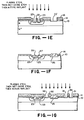
- a thin silicon nitride layer 14 of about 200A to 400A is deposited. This layer is also left in place in the finished device gate structure.
- the second masking step is carried out. That is, a photoresist mask 16 is put in place ( Figure lE), allowing for a plasma etch of the silicon nitride and a wet etch of the oxide to define where N diffusions will go, with the area 22 defining the eventual gate region. It should be noted that because of the processing steps taken to this point, the surface of the entire device has remained quite flat compared to known processes, providing easier fine line masking such as required to define area 22 (this will be less than two microns).
- a further advantage of this process is that the layers of oxide 10 and silicon nitride 14 are very thin, allowing good etch definition without undercutting. In contrast, in polysilicon gate processes, the gate etching must be carried out through layers 3,000 to 5,000A thick, which is about 10 times as thick as the layers used here.
- a phosphorus implant is carried out establishing the sources and drains 23.
- This is a major step saving because the photoresist 16 can be used both as an etch mask to define the junctions 23, and gate region 22; it is left in place, and can also be later used as an implant mask. It is important to note that this procedure specifically keeps phosphorus contamination out of the gate dielectric, which allows the possible use of very thin gate dielectrics, without fear of contamination diffusing thru the dielectric into the underlying channel.
- Channel stoppers 25 for P channel devices may be simultaneously defined with N channel devices, as shown in Figure lE.
- the photoresist layer 16 is stripped off.
- an oxygen ambient there is now a very controlled heating step to minimize lateral diffusion of the source and drain regions 23.
- oxide regions 26, 27 and 28 of about 1,000A are also grown over the source, drain and channel stop regions, the silicon nitride 14 effectively acting as an oxidation mask for the remainder of the surface, as shown in Figure 1F.
- the next, and only the third mask is the boron masking step which is used to define the adjacent P channel device having source, drain and gate regions 31 and 30.
- the photoresist 35 is used to mask against plasma etch, wet etch and boron implant, keeping contamination out of gate regions.
- lG channel stoppers 36 for N channel devices are simultaneously defined.
- Phosphorus is preferably implanted at a level of 2x10 15 /cm at 60 kev; and Boron at 1x10 /cm at 30 kev.
- first contact mask (Cl) is used to define and etch oxide where the first metal (Ml) layer will connect N or P diffusions.
- the resist is now cleaned off and first metal is deposited.
- This metal 46 is patterned to contact the source and drain junctions and span the gate regions as shown in Figure 1H.
- This process is self aligned because the oxide over the junctions is about 5 times thicker than the oxide-nitride sandwich over the channels (2000A vs 400A).
- M1 carries a signal from a P channel transister to an N channel transistor it will traverse channel stop regions 25 and 36 that are covered with about 2000A of oxide, and will traverse thin dielectric regions 47 of 400A thickness. To minimize stray capacitance of Ml traces, even though they might not be very long, it is important in the layout to have channel stop diffusions under Ml intraconnects wherever possible.
- a dielectric layer 48 of about 8000A is deposited. This can be oxide, nitride, a polymer, or a combination.
- the second contact mask (C2) is used to define and etch vias 49 through this dielectric in those places where it is desired that second metal (M2) should connect M1.
- the resist is cleaned off and M2 is deposited, patterned and etched. This metal is usually made thicker than the first metal (10,000A vs 5,OOOA) to help ensure reliable traversing of Ml steps by M2.
- guard bands 36 around the N channel devices are implanted.
- the result is the efficient use of process steps with guard bands encircling adjacent channel devices of both N and P types, providing high field thresholds in a scaled, self-aligned dual metal gate process.
- the gate regions get no doping, boron or phosphorus, and are kept clean so that there is no possibility of doping into the channel.
- diffusion is carried out at reduced temperatures so that short channels can be achieved.
Landscapes
- Metal-Oxide And Bipolar Metal-Oxide Semiconductor Integrated Circuits (AREA)
- Element Separation (AREA)
Applications Claiming Priority (2)
| Application Number | Priority Date | Filing Date | Title |
|---|---|---|---|
| US54395583A | 1983-10-20 | 1983-10-20 | |
| US543955 | 1995-10-17 |
Publications (2)
| Publication Number | Publication Date |
|---|---|
| EP0141571A2 true EP0141571A2 (de) | 1985-05-15 |
| EP0141571A3 EP0141571A3 (de) | 1987-01-07 |
Family
ID=24170210
Family Applications (1)
| Application Number | Title | Priority Date | Filing Date |
|---|---|---|---|
| EP84307075A Withdrawn EP0141571A3 (de) | 1983-10-20 | 1984-10-16 | Verfahren zum Herstellen eines CMOS mit einer Zwei-Ebenen-Metallisierung unter Verwendung einer verringerten Anzahl von Masken |
Country Status (2)
| Country | Link |
|---|---|
| EP (1) | EP0141571A3 (de) |
| JP (1) | JPS60143657A (de) |
Cited By (3)
| Publication number | Priority date | Publication date | Assignee | Title |
|---|---|---|---|---|
| US4925806A (en) * | 1988-03-17 | 1990-05-15 | Northern Telecom Limited | Method for making a doped well in a semiconductor substrate |
| GB2447136A (en) * | 2007-02-27 | 2008-09-03 | Ceres Ip Co Ltd | Fuel Cell Stack Hood |
| CN111584485A (zh) * | 2020-05-12 | 2020-08-25 | 杰华特微电子(杭州)有限公司 | 半导体器件及其制作方法 |
Family Cites Families (5)
| Publication number | Priority date | Publication date | Assignee | Title |
|---|---|---|---|---|
| US3983620A (en) * | 1975-05-08 | 1976-10-05 | National Semiconductor Corporation | Self-aligned CMOS process for bulk silicon and insulating substrate device |
| US4043025A (en) * | 1975-05-08 | 1977-08-23 | National Semiconductor Corporation | Self-aligned CMOS process for bulk silicon and insulating substrate device |
| US4047284A (en) * | 1975-05-08 | 1977-09-13 | National Semiconductor Corporation | Self-aligned CMOS process for bulk silicon and insulating substrate device |
| US4047285A (en) * | 1975-05-08 | 1977-09-13 | National Semiconductor Corporation | Self-aligned CMOS for bulk silicon and insulating substrate device |
| US4217149A (en) * | 1976-09-08 | 1980-08-12 | Sanyo Electric Co., Ltd. | Method of manufacturing complementary insulated gate field effect semiconductor device by multiple implantations and diffusion |
-
1984
- 1984-10-16 EP EP84307075A patent/EP0141571A3/de not_active Withdrawn
- 1984-10-19 JP JP59220340A patent/JPS60143657A/ja active Pending
Cited By (6)
| Publication number | Priority date | Publication date | Assignee | Title |
|---|---|---|---|---|
| US4925806A (en) * | 1988-03-17 | 1990-05-15 | Northern Telecom Limited | Method for making a doped well in a semiconductor substrate |
| GB2447136A (en) * | 2007-02-27 | 2008-09-03 | Ceres Ip Co Ltd | Fuel Cell Stack Hood |
| GB2447136B (en) * | 2007-02-27 | 2009-02-18 | Ceres Ip Co Ltd | Fuel cell stack flow hood |
| US8642227B2 (en) | 2007-02-27 | 2014-02-04 | Ceres Intellectual Property Company | Fuel cell stack flow hood |
| CN111584485A (zh) * | 2020-05-12 | 2020-08-25 | 杰华特微电子(杭州)有限公司 | 半导体器件及其制作方法 |
| CN111584485B (zh) * | 2020-05-12 | 2023-06-23 | 杰华特微电子股份有限公司 | 半导体器件及其制作方法 |
Also Published As
| Publication number | Publication date |
|---|---|
| JPS60143657A (ja) | 1985-07-29 |
| EP0141571A3 (de) | 1987-01-07 |
Similar Documents
| Publication | Publication Date | Title |
|---|---|---|
| US4244752A (en) | Single mask method of fabricating complementary integrated circuits | |
| US4312680A (en) | Method of manufacturing submicron channel transistors | |
| US4319395A (en) | Method of making self-aligned device | |
| US4422885A (en) | Polysilicon-doped-first CMOS process | |
| EP0894339B1 (de) | Siliciumkarbid-cmos und herstellungsverfahren | |
| US5688722A (en) | CMOS integrated circuit with reduced susceptibility to PMOS punchthrough | |
| US4825278A (en) | Radiation hardened semiconductor devices | |
| US6010929A (en) | Method for forming high voltage and low voltage transistors on the same substrate | |
| US4943537A (en) | CMOS integrated circuit with reduced susceptibility to PMOS punchthrough | |
| KR900008207B1 (ko) | 반도체기억장치 | |
| US4891328A (en) | Method of manufacturing field effect transistors and lateral bipolar transistors on the same substrate | |
| EP0104233A1 (de) | Verfahren zur herstellung komplementärer halbleitervorrichtungen | |
| US4663825A (en) | Method of manufacturing semiconductor device | |
| JP2010500765A (ja) | Soi又はバルクシリコンの何れか内の内蔵バックゲートを有するjfet | |
| EP0399231B1 (de) | Verfahren zur Herstellung eines Halbleiterbauteils | |
| US4471523A (en) | Self-aligned field implant for oxide-isolated CMOS FET | |
| KR0128339B1 (ko) | Cmos 기술을 이용하는 바이폴라 트랜지스터 제조방법 | |
| US5242849A (en) | Method for the fabrication of MOS devices | |
| US4517731A (en) | Double polysilicon process for fabricating CMOS integrated circuits | |
| CA1191973A (en) | Process for making complementary transistors | |
| GB2078443A (en) | Fabricating memory cells in semiconductor integrated circuits | |
| KR930005508B1 (ko) | 반도체장치 및 그 제조방법 | |
| KR950008257B1 (ko) | 모스(mos) 트랜지스터 및 그 제조방법 | |
| US4720739A (en) | Dense, reduced leakage CMOS structure | |
| KR19980018188A (ko) | 비정질화된 폴리실리콘을 사용하는 서브미크론 마이크로일렉트로닉스 응용을 위한 자기 정렬 POCl₃제조 방법 |
Legal Events
| Date | Code | Title | Description |
|---|---|---|---|
| PUAI | Public reference made under article 153(3) epc to a published international application that has entered the european phase |
Free format text: ORIGINAL CODE: 0009012 |
|
| AK | Designated contracting states |
Designated state(s): DE FR GB |
|
| PUAL | Search report despatched |
Free format text: ORIGINAL CODE: 0009013 |
|
| AK | Designated contracting states |
Kind code of ref document: A3 Designated state(s): DE FR GB |
|
| STAA | Information on the status of an ep patent application or granted ep patent |
Free format text: STATUS: THE APPLICATION IS DEEMED TO BE WITHDRAWN |
|
| 18D | Application deemed to be withdrawn |
Effective date: 19870430 |
|
| RIN1 | Information on inventor provided before grant (corrected) |
Inventor name: WANLASS, FRANK MARION |