EP0140158B1 - Dispositif et méthode pour la conversion d'un nombre binaire en un nombre sous un format décimal - Google Patents
Dispositif et méthode pour la conversion d'un nombre binaire en un nombre sous un format décimal Download PDFInfo
- Publication number
- EP0140158B1 EP0140158B1 EP84111464A EP84111464A EP0140158B1 EP 0140158 B1 EP0140158 B1 EP 0140158B1 EP 84111464 A EP84111464 A EP 84111464A EP 84111464 A EP84111464 A EP 84111464A EP 0140158 B1 EP0140158 B1 EP 0140158B1
- Authority
- EP
- European Patent Office
- Prior art keywords
- decimal
- partial sum
- bit
- binary
- digit
- Prior art date
- Legal status (The legal status is an assumption and is not a legal conclusion. Google has not performed a legal analysis and makes no representation as to the accuracy of the status listed.)
- Expired
Links
Images


Classifications
-
- H—ELECTRICITY
- H03—ELECTRONIC CIRCUITRY
- H03M—CODING; DECODING; CODE CONVERSION IN GENERAL
- H03M7/00—Conversion of a code where information is represented by a given sequence or number of digits to a code where the same, similar or subset of information is represented by a different sequence or number of digits
- H03M7/02—Conversion to or from weighted codes, i.e. the weight given to a digit depending on the position of the digit within the block or code word
- H03M7/06—Conversion to or from weighted codes, i.e. the weight given to a digit depending on the position of the digit within the block or code word the radix thereof being a positive integer different from two
- H03M7/08—Conversion to or from weighted codes, i.e. the weight given to a digit depending on the position of the digit within the block or code word the radix thereof being a positive integer different from two the radix being ten, i.e. pure decimal code
Definitions
- This invention relates to an apparatus and method for converting a number in binary format to a decimal format for data processing systems.
- the other method of representing numbers is to represent them in some type of decimal format.
- the decimal format commonly used is to have each decimal digit represented by four or more bits with the bits being binary encoded to represent the values of 0 to 9 decimal.
- Representing numbers in the decimal format has two disadvantages. First, as the number gets larger, more bits are required to represent a number in a decimal format than in a binary format. Second, performing decimal arithmetic operations is more complex and generally slower than binary operations because there are discontinuities at the boundaries between decimal digits which are not present between binary digits.
- using the binary coded decimal notation system allows the data processing system to work in the same number base as the user. To combine advantages an efficient method for converting binary numbers into decimal numbers is needed.
- the apparatus shown in this article uses shift registers for storing and shifting the binary number and the partial decimal result, respectively. This method, however, is ineffective as it must work through all bits of the binary number and, for each bit, all the decimal digits of the partial result including zero digits at the high end of the decimal partial sum must be doubled. Thus, this method does not allow to take into account leading zeros of the binary number and the development, digit for digit, of the decimal partial result.
- the invention eliminates leading zeros of the binary number. Therefore, all conversions steps related to these leading zeros are avoided.
- a further speed advantage is achieved by directing the doubling process of the decimal partial result for each examined bit only to the active decimal digits of the partial result that is only to the digit positions which store values that have already been developed during the conversion process. More significant decimal digits of the partial result are only comprised in the doubling process when a carry from the lower digit has been stored into them.
- Figure 1 illustrates the overall data processing system in which the present invention may be used. More particularly, Figure 1 shows a main memory subsystem 10, a central processing unit (CPU) 20 and an input/output (I/O) unit 40.
- the main memory subsystem 10 consists of three metal oxide semiconductor modules 12, 14 and 16. The three modules are interfaced to the central processor unit 20 and the input/output unit 40 via main bus 26.
- the main bus 26 gives the capability of providing access to and control of all memory modules and input/output units.
- the central processing unit 20 executes word oriented software instructions that operate on fixed and variable length fields.
- the basic unit of information in the central processor is a 16-bit word consisting of two 8-bit bytes (see Figure 5).
- a 16-bit word can also be broken into four 4-bit nibbles (see Figure 6).
- These words of information are used in groups of one, two or more for basic instructions (see Figure 7 for an example of one of the instruction formats) or fixed or floating point binary operands (data).
- These words are also used in groups of one or more words for commercial instructions (see Figures 8C-1 thru 8C-3).
- Bytes are also used in variable length fields as decimal or alphanumeric operands (data).
- CPU 20 is comprised of microprocessor (MPU) 30, monitor logic 22, Read Only Storage (ROS) 24 and commercial instruction logic (CIL) 28.
- Microprocessor 30 is an NMOS, 16-bit chip capable of arithmetic, logic, and control operations, driven by a 48-bit external microinstruction words which in the preferred embodiment are contained in ROS 24.
- the MPU 30 design permits the execution of the CPU 20 basic software instruction repertoire which operates on fixed and floating point binary data.
- Commercial instruction logic (CIL) 28 is used in conjunction with MPU 30 to permit the execution of the CPU 20 commercial software instruction repertoire which operates on decimal and alphanumeric data with the MPU 30 under the control of bits 0-47 of a 56-bit external microinstruction word contained in ROS 24.
- Microprocessor 30 is designed to directly control input/output (I/O) and memory operation for ease in integrated system designs.
- the MPU 30 design permits greater control and integration by use of a 48-bit external microinstruction word that provides true horizontal microprogramming allowing up to 12 simultaneous micro-operations per 48-bit microinstruction word.
- the MPU 30 design also permits 8 external hardware interrupts which generate vectors to microprogram routines as well as allowing 5 external software interrupts that are handled under firmware control.
- MPU 30 provides for 10 external monitor bits originated in monitor logic 22 that are sensed and controlled by sophisticated test branch and major branch operations by logic within microprocessor control area 36 which allows for sophisticated branching operations to be performed within the firmware. Four of these ten external monitor bits are set by CIL 28 to control test branch and major branch operations of MPU 30 when it and CIL 28 are used together to execute a commercial software instruction of CPU 20.
- Microprocessor 30 is comprised of 5 major internal hardware logic areas as shown in Figure 1.
- the five major logic areas are the data manipulation area 32 which includes the arithmetic logic unit (ALU), the memory management unit (MMU 34), the control area 36, the processor bus 37, and internal bus 38.
- ALU arithmetic logic unit
- MMU 34 memory management unit
- control area 36 the control area 36
- processor bus 37 the processor bus 37
- internal bus 38 internal bus
- the bus 37 consists of 20 address/data lines, one memory address violation line and three general purpose control lines. Bus 37 is connected to main bus 26 and is used to provide addresses to the main memory 10 and input/output unit 40 and to receive and send data to main memory 10 and input/output unit 40.
- Internal bus 38 is the major path for communications of information between the other four areas of the microprocessor chip. Internal bus 38 is 20-bit wide. There are 12 sources of information to internal bus 38 under control of the 11 micro-ops within the 48-bit microinstruction word. The ALU is the default source to internal bus 38 if none of the eleven defined micro-ops are used.
- the data manipulation area 32 performs arithmetic and logic operations on data and does memory address generation.
- the control area 36 of MPU 30 is logically divided into 3 areas: input latches for control, testable registers, and the next address generation.
- the MMU 34 section of MPU 30 is comprised primarily of: a register file, a 12-bit address for base relocation, a 9-bit comparator for checking the size of a memory segment, several 2-bit ring comparators for evaluating access rights to a given segment, and storage flip-flops for indicating potential memory violations.
- the MMU 34 translates the software logical address containing a segment number, a block number and an offset value presented by internal bus 38 into a physical address which is placed on bus 37 which in turn is transmitted to main memory 10 via main bus 26.
- CPU 20 executes software programs, the instructions of which are fetched from main memory 10, and performs arithmetic and logical operations on data also contained in main memory 10.
- the software program executed by CPU 20 has the ability to manipulate general and base address registers that are software visible and the current software instruction is pointed to by a program counter. These general registers, base address registers and program counter, which are visible to the software being executed by CPU 20, are physically contained within the data manipulation area 32 of MPU 30.
- CPU 20 of Figure 1 Detailed operation of CPU 20 of Figure 1 is controlled by MPU 30 under the control of microinstructions stored in ROS 24.
- Each location in ROS 24 can be interpreted as controlling one microprocessor machine cycle.
- the contents are decoded by control area 36 resulting in a specific operation within MPU 30.
- microinstruction sequences are obtained that can perform a specific operation or software instruction associated with CPU 20.
- certain bits within the operation code field of the software instruction are used to determine the starting address of the microinstruction routine contained within ROS 24.
- MPU 30 The testing of certain flip-flops which are set or reset by software instruction decoding done by MPU 30 allow the microprocessor to branch to a more specific microinstruction sequence within ROS 24 when necessary.
- MPU 30 branches to that portion of ROS 24 which contains 56-bit microinstruction words so that bits 0-47 are used to control the operation of microprocessor 30 and bits 48-55 are used to control the operation of CIL 28.
- CIL 28 is described in greater detail with reference to Figure 2 below.
- the input/output controller 42 is that portion of the input/output unit 40 which completes a data path from a peripheral device 44 to main memory 10 via main bus 26. I/O controller 42 provides a path thru which the peripheral commands are initiated, in addition to controlling resulting data transfers.
- the MPU 30 has the ability to perform various shift operations (i.e., open/closed, arithmetic/logical, left/right) on either 16-bit or 32-bit operands.
- ROS 24 may be a read only memory (ROM) or a random access memory (RAM) or any other form of memory device capable of holding microinstructions.
- the ROS 24 contains the microinstructions (or control words) which are used by MPU 30 and CIL 28 to control the operation of central processing unit and more particularly to execute the software instructions of CPU 20. For each microprocessor machine cycle, a control word is fetched out of ROS 24.
- ROS 24 is coupled to a ROS data register which receives bits 0-47 of the microinstruction word fetched from read only storage 24.
- Each microinstruction contains an address portion and a command portion.
- the address portion in the microinstruction word identifies the address of the next location to be read from read only storage 24 which will be the next microinstruction to be executed by MPU 30.
- the command portion of the microinstruction identifies the operations to be performed by the MPU 30 and CIL 28 during the execution of the current microinstruction.
- the address portion of the microinstruction word may be contained in a predetermined number of bits, for example, in the preferred embodiment it is contained in bits 0 thru 12 of the microinstruction word (see Figure 3).
- the command portion of the microinstruction may also be contained in a predetermined number of bits, for example, in the preferred embodiment it is contained in bits 13 thru 47 which control the operation of MPU 30 and in bits 48 thru 55 which, when present, along with bits 35 thru 47 control the operation of CIL 28 (see Figure 3).
- the command portion may be further broken down into a number of fields which comprise subcommands of the microinstruction.
- FIG 3 illustrates the microinstruction word fields of MPU 30 of the preferred embodiment.
- This microinstruction word is comprised of 56 bits (bits 0-55). Bits 0-47 which control MPU 30 will be discussed now and bits 48-55 which control commercial instruction 28 will be discussed later with reference to Figure 2.
- Bits 0 thru 12 are used as the ROS address field
- bits 13 thru 17 are used to select registers in a register file
- bits 18 thru 22 are used to control the arithmetic and logic functions of the ALU and the inputs to its ports
- bits 23 thru 25 are used as bus control
- bits 26 thru 30 are used as a register modification field
- bits 31 thru 33 are used as memory management unit control
- bit 34 is used to inhibit the occurrence of a hardware interrupt
- bits 35 thru 47 are used as a special control field.
- the special control field (RDDT bits 35 thru 47) is used to modify as well as supplement certain of the other fields in the microinstruction word.
- the special control field provides up to three simultaneous microcommands during a given microcycle.
- the special control field is divided into 4 subfields (Athru D) as illustrated in Figure 3. With the interpretation of some of the subfields dependent upon the contents of other subfields.
- the 48 bits of the microinstructions are loaded into the ROS data register at the beginning of the execution of the microinstruction. These 48 bits are referred to as signals RDDTOO thru RDDT47.
- the ROS address field contains 13 bits (RDDTOO thru RDDT12) and is used to generate the address of the next firmware step in a given microprogram sequence.
- Figure 2 illustrates the CIL 28, of Figure 1 in greater detail.
- Figure 2 also illustrates MPU 30, read-only storage 24 and monitor logic 22.
- the number next to the upper right-hand corner of the blocks represents the number of bits of information contained in the register represented by the block and the numbers within parentheses next to signal lines represents the number of parallel signals transmitted over the signal path.
- CIL 28 is used in conjunction with MPU 30 to perform the commercial software instructions of CPU 20 which do decimal arithmetic operations on decimal data and editing operations on alphanumeric data strings.
- CIL 28 consists primarily of random access memory (RAM) 1 81, RAM 2 96 and decimal adder/subtractor PROM (DALU) 84, all of which operate under the control of CIL control area 100.
- RAM random access memory
- DALU decimal adder/subtractor PROM
- CIL control area 100 is used to decode the bits within the microinstruction word which control CIL 28.
- CIL control area receives bits 35 thru 47 of the microinstruction word shown as the special control field in Figure 3, which are also used to control the operation of MPU 30 and in addition it receives bits 48 thru 55 which are dedicated to the control of CIL 28. Decoding of these microinstruction bits associated with the commercial instruction logic is performed by CIL control area 100 which produces control signals which are distributed thruout CIL 28 to control the enabling and disabling and the selection of the various registers, gates and multiplexers.
- Data is transmitted between microprocess 30 and CIL 28 over a 16-bit wide data path which connects bus 37 of MPU 30 to transceivers (XCVR) 97.
- XCVR transceivers
- the output of XCVR 97 can be latched into data-in register 98 which is also 16 bits wide.
- XCVR 97 can not only load data-in register 98 from the output of bus 37, but can also be used to transfer the output of RAM 2 data register 88 from XCVR 97 to bus 37.
- This data path from the output of RAM 2 data register 88 which is 16 bits wide, besides being connected into XCVR 97 can also be used to load data-in register 98 and thereby provide the means for loading the output of RAM 2 96 into RAM 1 81 or back into RAM 2 96.
- CIL 28 is used to perform a commercial software instruction which requires two operands, operand 1 is usually stored in RAM 1 81 and operand 2 is stored in RAM 2 96 and the output of the operation is stored back into RAM 2 96.
- DALU 84 As indicated, the arithmetic and logic unit functions of CIL 28 are performed by DALU 84.
- DALU 84 generates the result by using its four inputs (2 4-bit operands, 1 bit of carry-in and a 1-bit indicator indicating whether this is an add or subtract operation) to form a 10-bit address which is used to fetch and 8-bit data word which contains a 4-bit arithmetic result of the addition or subtraction and four indicators (one bit of carry-out, one bit to indicate whether one of the operands is an illegal value, a bit indicating whether the result is equal to zero, and a bit indicating whether the result is equal to nine).
- Table 1 The coding of DALU 84 is shown in Table 1.
- Table 1 shows the encoding of the 10-bit address.
- the most significant bit in the 10-bit address which has a value of 512, is used as an indicator as to whether the operation being performed is an addition or subtraction.
- address bit 512 is equal to a binary ZERO
- a subtraction is to be performed
- binary ONE an addition is to be performed.
- the next address bit having a value of 256, is used to indicate whether a carry in from the previous decimal digit is to be used in calculating the result and when a binary ZERO indicates that the previous digit did not generate a carry-out and when a binary ONE indicates that the previous digit did generate a carry-out.
- the next four address bits bits having a value of 128, 64, 32 and 16, are used to represent the four bits of operand 2 at the B port of DALU 84 and the last four bits having values of 8,4,2 and 1 are used to indicate the values of operand 1 at the A port of DALU 84.
- the 8-bit data word retrieved from PROM 1 as addressed by the 10-bit address is coded with the result as indicated in Table 1.
- the four lower bits of the data word (bits 3 thru 0) contain the 4-bit decimal result of the addition or subtraction.
- the other four bits of the data word contain the four indicators which are output by DALU 84.
- the 4-bit indicators are encoded such that bit 7 of the data word (labelled "CRO” in Table 1), when a binary ZERO, indicates that there is no carry-out and, when a binary ONE, indicates that there was a carry-out.
- Bit 6 (labelled “ILL” in Table 1), when a binary ZERO, indicates that both operand 1 and operand 2 were legal decimal values and when a binary ONE, indicates that one or the other of operand 1 or operand 2 contained an illegal decimal value (i.e., a hexadecimal value of from A thru F)
- bit 5 (labelled “EO” in Table 1) indicates when a binary ONE that the arithmetic result is equal to zero and when a binary ZERO that the arithmetic result is not equal to zero
- bit 4 (labelled “E9” in Table 1) when a binary ONE indicates that the arithmetic result equal nine and when a binary ZERO indicates that the arithmetic result does not equal nine.
- the four indicator bits are held by indicators 85 and are also an input into monitor MUX 80 and the carry-out bit is input into DALU 84 as the carry-in bit.
- the 4-bit decimal arithmetic result is one input into result/zone MUX 91.
- the ability to detect whether either of the two operands contains a value greater than 9 is very useful in that it allows the DALU 84 to detect the case of an illegal operand which has a decimal digit which is represented by four bits and therefore can have values of from A thru F hexadecimal which are illegal.
- the ability for the DALU 84 to detect illegal decimal operands as part of the addition/subtraction process eliminates the need for a separate precheck of the operands by a prescan of the operands prior to introducing them into the ALU.
- Sign detector PROM 78 is similar in operation to DALU 84. Sign PROM 78 uses the nine input bits to address a 4-bit data word which indicates the sign of the operands used in an arithmetic operation. Of the nine bits used to address the 4-bit data words of the PROM 78, three bits come from data-in register 98, 4 bits from sign multiplexer 77, and two bits (PACKD) and overpunch (OVPUN) from CIL control area 100. The output of PROM 78 can be gated to monitor logic 22 for inputting input MPU 30 via monitor MUX 80.
- the four bits output by PROM 78 indicate whether the sign is positive or negative, whether it is an illegal sign atom whether the sign is an overpunch sign, and whether it is an overpunched zero.
- the resultant sign can be .tested by the MPU 30 firmware examining the four monitor bits.
- the generation of the sign result is complex in that the CPU 20 allows decimal numbers to be represented in either a packed or unpacked format with trailing or leading signs and overpunch signs.
- RAM 1 zero MUX 82 at the output of RAM 1 81 and RAM 2 zero MUX 90 at the output of RAM 2 96 are used to allow the commercial instruction logic firmware to effectively zero out the output of RAM 1 and RAM 2 respectively so that the operand in the other RAM can effectively be added or subtracted from zero.
- RAM 2 data register 88 holds the 16-bit output of RAM 296.
- RAM 2 nibble MUX 89 is used to select the one of the four 4-bit nibbles held in RAM 2 data register 88 so that the appropriate nibble can be gated into RAM 2 zero MUX 90 or into double MUX 83 in preparation of adding or subtracting a nibble from RAM 296 with a nibble from RAM 1 81 in DALU 84.
- Nibble 0 MUX 92, nibble 1 MUX 93, nibble 2 MUX 94, and nibble 3 MUX 95 are used to either allow a 16-bit quantity to be loaded in from data-in register 98 into RAM 2 96 or to allow a 4-bit nibble from result/zone MUX 91 into the appropriate 4-bit nibble of the 16-bit word stored in RAM 2 96 under firmware control.
- Result/zone MUX 91 is used to determine whether the 4-bit result from DALU 84 or the four zone bits are to be written into a nibble within RAM 2 96.
- each four bits of data in the decimal value represent a decimal digit having the value from zero thru nine.
- each decimal digit is represented by an eight bits in which the most significant (left) four bits of the 8-bit field represent a zone field having a value of 3 hexadecimal and the least significant (right) four bits represent the decimal values 0 thru 9.
- each decimal digit is represented by an 8-bit field which contains the ASCII code for the decimal digit. Therefore, result/zone MUX 91 can select between the 4-bit result from DALU 84 (which can have a value from 0 thru 9) or the four zone bits which are preset to 0011 binary (3 hexadecimal). For example, the decimal value 76 when stored in a packed field is stored in eight bits with the most significant 4-bit nibble containing the value 7 and the least significant 4-bit nibble containing the value 6.
- 76 decimal When the same value of 76 decimal is stored in an unpacked field, it is stored in two 8-bit bytes with the left most 4-bit nibble of each byte being a 4-bit zone field which contains the hexadecimal value of three and the right 4-bit nibble in each byte containing the decimal value of 7 in the left byte and 6 in the right byte. Therefore, the value of 76 decimal in a packed decimal field is represented by the 8-bit field of 76 hexadecimal and in an unpacked field it is represented by a 16-bit field containing 3736 hexadecimal.
- Double MUX 83 allows one input of DALU 84 to be selected between four bits from RAM 1 81 or four bits from RAM 2 96.
- double MUX 83 selects one input of DALU 84 to be four bits from RAM 2 96, the effect is that the output of DALU 84 is double the value of the four bits from RAM 2 because in this case both inputs to the DALU 84 will be from RAM 2. This provides a very convenient method of multiplying by two the operand stored in RAM 2 96.
- RAM 1 81 and RAM 2 96 contain 16-bit data words, with RAM 1 containing 16 such 16-bit words and RAM 2 containing 256 16-bit words, there are other distinctions between these two RAMs.
- RAM 1 normally holds operand 1 and may be written into only on a 16-bit word basis. That is, when information is written into RAM 1 from data-in register 98, all four nibbles of the 16-bit word are written to.
- the output of RAM 1 is always a single 4-bit nibble which is presented at one of two inputs to RAM 1 zero MUX 82.
- the word which is read from RAM 1 81 is controlled by RAM 1 address counter 75 and the nibble which is enabled into one input of RAM 1 zero MUX 82 is controlled by nibble out control 76.
- RAM 1 address counter 75 also receives inputs from nibble out control 76 such that consecutive decimal digits may be accessed from RAM 1 by either incrementing or decrementing a nibble counter in nibble out control 76 which in turn either increments or decrements the word counter in RAM 1 address counter 75 each time that four nibbles have been accessed.
- RAM 2 96 has the ability to be written into as one 16-bit word or the ability to write any one of the four individual nibbles.
- the 16-bit word to be written into RAM 2 96 comes from data-in register 98 which can be loaded from bus 37 or from the output of RAM 2 data register 88.
- Individual nibbles are written into RAM 2 96 from the output of result/zone MUX 91 with the value of the nibble being either the result of the DALU 84 or a 4-bit zone field containing the hexadecimal value of 3.
- Nibble write control 86 determines whether a 16-bit word is written into RAM 2 96 or whether one or four individual nibbles is written into RAM 2 96.
- RAM 2 address counter 87 determines the 8-bit word address that is used to address RAM 2 96 for either a read or write operation.
- RAM 2 address counter 87 receives an input from nibble write control 86 so that consecutive nibbles may be accessed from RAM 2 96. Each time the four nibbles have been accessed, RAM 2 address counter 87 is either incremented or decremented to get to the next word which contains the next consecutive nibble.
- a read from RAM 2 96 results in a 16-bit data word being read out and latched into RAM 2 data register 88.
- the particular nibble to be accessed in a 16-bit data word is controlled by RAM 2 nibble MUX 89 which selects one of the four nibbles to be output into RAM 2 zero MUX 90 and double MUX 83.
- a read in RAM 1 results in only four bits of one nibble being output with the other twelve bits of the three nibbles not being enabled.
- the enabling of the nibble which is read from RAM 1 81 is controlled by nibble out control 76.
- the 16-bit word read from RAM 2 96 into RAM 2 data register 88 can be written back into RAM 2 96 via data-in register 98 or it can be written into RAM 1 81 via data-in register 98 under firmware control.
- nibble write control 86 besides controlling which one of four nibbles is write enabled into RAM 2 when a single nibble is being written into, also controls the selection of which one of four nibbles will be output by RAM 2 nibble MUX 89. When a 16-bit word is written into RAM 2 96, all four nibbles are write enabled by nibble write control 86.
- RAM 1 81 and RAM 2 96 are determined by their use by the firmware.
- RAM 1 81 is used primarily to hold operand 1 which, in the CPU of the preferred embodiment, may be a decimal number of from 1 thru 31 decimal digits including the sign. Therefore, to accommodate a 31 digit decimal number, sixteen words of 16 bits each are required in order to be able to hold the 31 bytes of the maximum decimal number if the number is an unpacked decimal number having zone bits associated with each decimal digit.
- RAM 2 96 besides normally holding operand 2 is divided into eight segments with each segment being used to either hold an operand or as a working register. For example, in the case of a decimal divide, the segments of RAM 2 96 are used to hold an original copy of operand 1, an original copy of operand 2, a packed copy of operand 2, the quotient and partial products.
- microinstruction word which control the operation of CIL 28 will now be described with reference to Figure 2 and Figure 3 and Table 2 thru Table 6.
- a microinstruction word is read from ROS 24 either 48 bits or 56 bits are retrieved. If the address is within the first 2K of ROS (i.e., addressed 0 thru 2047) a 48-bit microinstruction word is retrieved and if the address is from 2048 thru 4095 a 56-bit microinstruction word is retrieved.
- bits 0 thru 47 of microinstruction word are always latched into a ROS data register in control area 36 for decoding and controlling the operations of MPU 30.
- the special control field of the microinstruction word bits 35 thru 47, are also latched into ROS SCF register 101 of CIL control area 100 (see Figure 2).
- subfield A of the special control field is used to enable some of the mops controlled by subfields B and C.
- the requirement that certain of the mops specified in subfields B and C of the special control field are enabled only if subfield A contains a binary 110 is necessary in order to inhibit CIL 28 from performing certain mops which would otherwise interfere with the mops being performed by MPU 30.
- Zero MUX 102 is used to force binary ZEROs into ROS CIL register 103 when the MPU 30 addresses a firmware location in the lower 2K of ROS 24 (see Table 5 and Table 6) thereby inhibiting CIL 28 from performing any operation when a microinstruction word has been retrieved from ROS 24 which does not contain bits RDDT48 thru RDDT55 (see Figure 3).
- CIL control area 100 the various control signals from CIL control area 100 are applied to the various logic elements of CIL 28 during each microinstruction execution cycle. It will also be understood that the clock signals from MPU 30 provide appropriate timing signals in a conventional manner to the CIL 28 to provide appropriate timing therefor. In order not to confuse the drawings, the particular timing and control signals fed to various elements are not shown in Figures 1 and 2, but are assumed to be provided where appropriate.
- RDDT42 thru RDDT44 control the following mops.
- a binary 000 no operation is performed by CIL 28.
- the PACKD signal input into sign detection PROM 78 is made a binary ZERO and is used to address the portion of the sign PROM 78 which contains the coding for packed decimal sign types.
- signal OVPUN becomes a binary ZERO and is used to address the portion of the PROM 78 which contains the encoding for overpunched signs.
- DALU 84 When a binary 011, a subtract operation is performed by DALU 84 by forcing the signal ADD/SUB which is one of its inputs to be a binary ZERO.
- the equal zero and equal nine indicators in indicators 85 are reset to zero.
- RAM 1 address counter 75 When a binary 101, the address counter in RAM 1 address counter 75 is incremented by one such that the next word in RAM 1 81 is addressed thereby allowing one of four new nibbles to be input into RAM 1 zero MUX 82.
- the nibble enabled into RAM 1 zero MUX 82 is determined by nibble out control 76.
- RAM 1 address counter 75 When a binary 110, RAM 1 address counter 75 is decremented by one, addressing the next lower word in RAM 1 81 and making available at its output one of four new nibbles with the enabled nibble again being under the control of nibble output control 76.
- all four indicators in decimal indicators 85 are reset to binary ZERO thereby indicating that there is no carry, that the result is not equal to zero, that the result is not equal to nine, and that the result is not an illegal digit.
- the mops controlled by subfield E are illustrated in Table 5.
- nibble write control 86 When a binary 0011, a word address is loaded into RAM 1 address counter 75 and a nibble count is loaded into nibble output control 76 from data-in register 98 thereby allowing the specifying as to the word and the nibble which will be read from RAM 1 81.
- an initial address is loaded into RAM 2 address counter 87 from data-in register 98 thereby controlling which word will be written into or read from RAM 2 96.
- an initial nibble count is loaded into nibble write control 86 thereby controlling which nibble will be write enabled into RAM 2 96.
- the nibble counter within nibble write control 86 also controls which of the four nibbles from RAM 2 data register 88 is enabled onto the outputs of RAM 2 nibble MUX 89.
- the address counter in RAM 2 address counter 87 and the nibble counter in nibble write control 86 are loaded from data in register 98 thereby controlling the word that is addressed within RAM 2 and the nibble which is write enabled into RAM 2 and the nibble which is selected at the output of RAM 2 nibble MUX 89.
- the word address contained in data-in register 98 is loaded into RAM 1 address counter 75 and RAM 2 address counter 87.
- the nibble count and data-in register 98 is loaded into the nibble out control 76 and into nibble write control 86 thereby allowing the selection of one of four nibbles in RAM 1 and RAM 2.
- the word address and the nibble count from data-in register 98 are loaded into RAM 1 address counter 75 and RAM 2 address counter 87 and nibble out control 76 and nibble write control 86 respectively.
- the nibble counter in nibble out control, 76 is incremented by one and if it changes from a nibble count of three to a nibble count of zero, the word counter in RAM 1 address counter 75 is also incremented by one. This allows nibbles to be consecutively addressed and after the four nibbles have been addressed from one word, the first nibble is addressed in the next word.
- the nibble counter in nibble out control 76 is decremented by one and if the count changes from zero to three, the word counter in RAM 1 address counter 75 is decremented by one thereby allowing consecutive nibbles to be addressed from right to left.
- the nibble counter in write control 86 When a binary 1100, the nibble counter in write control 86 is incremented by one and if the nibble counter goes from three to zero, the word counter in RAM 2 address counter 87 is also incremented by one thereby allowing consecutive nibbles to be addressed from left to right.
- the nibble counter in nibble write control 86 When a binary 1101, the nibble counter in nibble write control 86 is decremented by one and if the count goes from zero to three, the word counter in RAM 2 address counter 87 is also decremented by one to point to the next word in RAM 2 96. This decrementing of the nibble counter associated with RAM 2 by one allows consecutive nibbles in RAM 2 to be addressed from right to left.
- the nibble counter in nibble out control 76 is incremented by one as is the nibble counter in nibble write control 86 and when a counter go from three to zero, the corresponding word counter in RAM 1 address counter 75 and RAM 2 address counter 87 is also incremented by one thereby allowing consecutive nibbles to be addressed from left to right in RAM 1 and RAM 2.
- nibble counter in nibble out control 76 is decremented by one
- the nibble counter in nibble write control 86 is decremented by one
- RDDT52 thru RDDT55 is a binary 0000
- no operation is performed by CIL 28.
- XCVR 97 are enabled such that the data on bus 37 is available to data-in register 98 and data-in register 98 is clocked such that the information becomes available to CIL 28 at the output of data-in register 98.
- the XCVR 97 are enabled to transmit data from CIL 28 to MPU 30 such that the information in RAM 2 data register 98 is passed to bus 37.
- this mop clocks data-in register 98 such that the data from RAM 2 data register 88 is loaded into data-in register 98.
- the word address counter in RAM 2 address counter 87 is incremented by one thereby pointing to the next word within RAM 2 96. It should be noted that the incrementing and decrementing of the address counter for RAM 2 is controlled by subfield F and the incrementing and decrementing of the address counter for RAM 1 is controlled by subfield C so that the address counters of RAM 2 and RAM 1 can be incremented and decremented in parallel.
- the carry indicator in indicators 85 is set to a binary ONE.
- a test mode flop is set to indicate that a fault condition has occurred within CIL 28.
- XCVR 97 are enabled to receive data from bus 37 and data-in register 98 is clocked such that the data is latched in it and at the same time the word address counter in RAM 2 address counter 87 is incremented by one.
- XCVR 97 are enabled to receive the data from bus 37 and it is latched into data-in register 98.
- the address counter in RAM 2 address counter 87 is decremented by one such that the next lower word in RAM 2 96 is addressed. As in the previous mop, it is useful for allowing consecutive words in RAM 2 to be loaded from bus 37.
- XCVR 97 When a binary 1011, XCVR 97 are enabled to transmit the data from the output of RAM 2 data register 88 to bus 37 and at the same time this data is loaded into data-in register 98. In addition, the address counter in RAM 2 address counter 87 is incremented by one. When a binary 1100, XCVR 97 are enabled to to bus 37 to allow the outputting of data in RAM 2 data register 88 and at the same time the data is loaded into data-in register 98. In addition, the address counter in RAM 2 address counter 87 is decremented by one such that the next lower word in RAM 296 is pointed to. The mops specified by binary 1101, 1110 and 1111 are not used.
- the three different data types handled by the CIL 28 are: decimal data, alphanumeric data, and binary data.
- the decimal and binary data types are used to represent fixed point integer numeric values.
- the alphanumeric data type is used to represent alphabetic, numeric and punctuation of text information.
- the commercial software instructions of the CPU permit arithmetic operations on the decimal data and editing operations on alphanumeric data. These commercial software instructions are performed by CIL 28 in conjunction with MPU 30.
- Table 7 gives the size of an atom in bits as a function of the data type.
- Eight-bit atoms are also referred to as “bytes” and 4-bit atoms are also referred to as “nibbles”.
- Figure 5 illustrates the position of byte 0 and byte 1 within the 16-bit words of the preferred embodiment.
- Figure 6 illustrates the positions of nibble 0 thru nibble 3 in a 16-bit word.
- the bits are numbered 0 thru 15 with bit 0 being the most significant bit (MSB) and bit 15 being the least significant bit (LSB) as illustrated in Figures 5 and 6.
- Decimal data can be represented in either string (also referred to as unpacked) or packed form.
- the maximum length of a decimal operand is 31 atoms (i.e., if separate sign, then 30 digits plus sign).
- Decimal numbers are treated as integers with the decimal point assumed to be to the right of the least significant digit.
- a decimal operand can be signed or unsigned and when unsigned it is assumed to be positive.
- Zone bits are not checked by the hardware on input but will be set to 3 hexadecimal (0011 binary) on output.
- String decimal data can be signed or unsigned. When unsigned the operand is considered to be positive and its length refers only to digits. When signed, the operand can have either: leading separate sign, trailing separate sign, or trailing overpunched sign.
- the length of the operand also includes the sign character.
- decimal digits occupy four bits or one-half a byte position in memory (also referred to as nibbles). These digits can start and/or end on any half byte boundaries. The only valid codes for packed decimal digits are 0-9 otherwise an illegal character trap will result.
- Packed decimal data can be signed or unsigned.
- the operand When unsigned, the operand is considered to be positive and its length refers only to digits. When signed, the sign will be the least significant atom of the operand. The length of the operand will include the sign atom. Sign, when specified, can only be separate trailing; i.e., the rightmost atom of the operand field.
- Alphanumeric operands consist of ASCII 7-bit characters. Their maximum size is 255 characters except as specified otherwise. Each alphanumeric character atom occupies one 8-bit byte.
- Alphanumeric strings in memory can start and/or end or both on either odd or even byte boundaries.
- Binary operands can be either 16 bits long or 32 bits long (i.e., one or two words). They are 2's complement numbers and thus the most significant bit is the sign bit and the binary point is assumed to be to the right of the least significant bit.
- Binary operands in memory can start and/or end on either odd or even byte boundaries.
- the commercial software instructions of CPU 20 are classified as follows: numeric, alphanumeric, edit and branch.
- DISPLACEMENT specifies the software instruction by its displacement in number of words forward or backward.
- DDn D at a descriptor specifies the type, size and location of the operand.
- DD1 refers to the first data descriptor;
- DD2 refers to the second and
- DD3 refers to the third.
- Label 1 refers to the first data descriptor: Label 2 refers to the second and Label 3 refers to the third.
- a commercial software instruction can have from 1 to 3 operands which are defined by data descriptors.
- Data descriptors DDs are used to define the operand type, size and location in memory.
- Figure 8C-1 illustrates the format of a commercial software instruction using in-line data descriptors which describe the 1 to 3 operands used by the instruction.
- Figure 8C-2 illustrates the format of a commercial software instruction using remote data descriptors and
- Figure 8C-3 shows the format of a commercial software instruction using a combination of in-line and remote data descriptors.
- bits 12 thru 15 are binary ZEROs.
- a data descriptor can be either a; decimal DD, alphanumeric DD, or binary DD.
- Decimal DDs are implied by all numeric software instructions and the numeric edit instruction. Decimal DDs can refer to either string decimal or packed decimal data. The format of the DD is as shown in Figure 9 where:
- L specifies the length-of the operand in number of atoms.
- T specifies the data type: string or packed.
- CAS specifies the commercial address syllable.
- Alphanumeric DDs are implied by all alphanumeric software instructions and the alphanumeric edit software instruction.
- the format of the alphanumeric DD is somewhat similar to that shown in Figure 9 but need not be further described.
- EA effective address
- the CAS is a seven bit field of a data descriptor in which bits 9 thru 11 are used as an address modifier, bit 12 is generally used to indicate whether direct or indirect addressing is to be used, and bits 13 thru 15 are used to indicate a base register number.
- the definition of the commercial software instructions supports post indexing of data at the atom level.
- the index value is in atoms and it is automatically adjusted to correspond to the data type specified in the DD.
- Convert binary to decimal moves and converts the contents of binary DD1 and places the decimal string or packed result in the contents of DD2 (i.e., [DD1] converted and stored in [DD2]).
- DD2 i.e., [DD1] converted and stored in [DD2]
- the OV and SF commercial indicators are set as a function of the result.
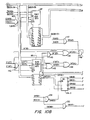
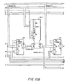
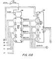
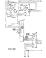
- Figure 10A primarily shows the structure of RAM 1 81 and its associated addressing logic
- Figure 10B primarily shows the structure of RAM 2 and its associated addressing logic
- Figure 10C primarily shows the structure of DALU 84 along with its inputs and outputs and indicators 85
- Figure 10D primarily shows the structure of CIL control area 100.
- the decimal arithmetic operations that are performed by CPU 20 are microprogrammed to take advantage of CIL 28 to reduce the execution time of the decimal commercial software instructions.
- the convert decimal to binary commercial software instruction is sped up by using the ability to address RAM 1 81 for left to right to strip leading zeros.
- the convert binary to decimal commercial software instruction is sped up by using the ability of the DALU 84 to have the same data fed to both inputs and by presetting the converted value receiving field to a zero digit and increasing the receiving field length as necessary (when a carry occurs) as the conversion progresses.
- microprocessor 30 and CIL 28 operate in parallel to perform the necessary mops under the control of microinstructions stored in ROS 24.
- Microinstruction bits 0 thru 47 are used to control the operation of MPU 30 and microinstruction bits 35 thru 55 be used to control the operation of CIL 28.
- the use of microinstruction bits 35 thru 47 to control MPU 30 or commercial instruction logic 29 depend on the value of special control field subfield A.
- MPU 30 is used to: read the software instructions from main memory 10, to decode the software instructions, to read the operands from main memory 10, to perform arithmetic, shifting and logical operations on binary data, and write the results of the operation back into main memory 10.
- CIL 28 is used to perform logic and shifting operations on decimal and alphanumeric data.
- the decimal partial sum is added to itself each time a bit within the binary number is examined with the carry into the least significant digit of the decimal partial sum being set equal to the bit of the binary number that is being examined.
- this process works, it can be time consuming because the decimal add of the partial sum must be performed for each digit within the binary number being converted such that if a binary number is a 32-bit binary number, 32 decimal adds of the partial sum must be performed.
- These additions can be quite long if the addition is performed on a partial sum that has as many decimal digits in it as required to hold the largest possible number represented by the length of the binary number (i.e. 2 to the 31 power plus a sign bit).
- an improved method is used which first strips off the leading zeros within the binary number such that if a binary number is represented in 16 bits and the most significant 8 bits are all zeros, the 8 first bits are stripped off thereby reducing the total number of decimal additions which need to take place on the partial sum.
- the length of the partial sum is initially set equal to one decimal digit and the length is adjusted only as the number of digits within the partial sum increases so that each addition of the partial sum only is required to do a decimal add on as many digits as required to hold the partial sum at any given instance.
- the binary to decimal conversion commercial software instruction takes the binary number given to it as operand 1 and it converts it to a decimal number and stores the result in the field specified for operand 2.
- a binary number of -37 will be converted to a decimal number which is to be placed in a packed decimal field with a trailing sign.
- negative binary numbers are represented in a two's complement form
- CBD Software Instruction Data descriptors DD1 and DD2 are decoded as follows (see Figure 9):
- Figure 11 is a flow chart of the microroutines used by CPU 20 to execute a CBD software instruction.
- the blocks in Figure 11 which are referred to by the names next to them, such as CBD-001, show at a gross level the functions performed by MPU 30 and CIL 28 to perform the software instruction. Some of these blocks may represent the execution of more than one 48 or 56-bit microinstruction, the form of which is shown in Figure 3.
- the CPU 20 examines the first word of the software instruction which is being executed to determine the type of operation to be performed.
- the CPU 20 then proceeds to decode the address syllable associated with data descriptor 1 to determine the main memory word address and the position within the word in which operand 1 begins. This front end processing of the software instruction then continues with the microprocessor branching to the CBD routine at block CBD-000.
- the binary to decimal conversion routine When the binary to decimal conversion routine is entered at CBD-000, it determines whether this is a first pass in which operand 1 is to be brought into the CPU or the second pass in which operand 2 is to be brought into the CPU. If it is the first pass, the firmware then branches to block CBD-001 which fetches operand 1 (the binary number to be converted) into MPU 30. Block CBD-001 then exits to the instruction front end routine which eventually returns to block CBD-000 to perform the second pass in which case block CBD-002 is entered. Block CBD-002 analyzes the data descriptor 2 to determine the starting and end positions of the operand 2 field which is to hold the converted number and the length of the field.
- Block CBD-003 then brings in operand 2 so that the neighbors may be saved when the converted number is stored into that field in main memory.
- Operand 2 which is the field in which the converted number is to be stored, is brought into segment 1 of RAM 2 such that at the end of block CBD-003, RAM 2 segment 1 contains the converted number field as follows:
- Block CBD-004 is then entered and a test of the sign of operand 1 binary is made. If the sign of the binary number to be converted is negative, block CBD-004 branches to block CBD-005 to perform a two's complement on the binary operand and to note that the sign of the result should be negative. Block CBD-005 then exits to block CBD-006 which sets up the appropriate bit counter to equal either 16-bits, if a single precision binary number containing 16 bits is to be converted, or equal to 32, if a double precision number containing 32 bits is to be converted. Block CBD-006 then exits to block CBD-009.
- block CBD-005 determines that the binary number is to be converted is a positive number
- block CBD-007 is entered and a flag is set to indicate that the result is positive.
- Block CBD-007 then exits to block CBD-008 which sets up a bit counter equal to 16, if it is a single precision binary number to be converted, to 32, if a double position binary number is to be converted.
- Block CBD-009 is then entered and the binary number within MPU 30 is then shifted to the left until the first non-zero binary bit is encountered and the length of the binary field which has to be converted, either 16 or 32, is adjusted to reflect the number of non-zero bits remaining in the binary number. If block CBD-009 determines that all bits within the binary number to be converted are zeros, block CBD-009 exits to the zero result routine, which is routine CBD-020. If the binary number to be converted is not zero, block CBD-009 after stripping off all leading zero bits then exits to block CBD-010 which puts a binary ZERO into the unit's position of the operand 2 field which will contain the converted binary number in a decimal format. At the end of block CBD-010, the operand 2 field in RAM 2 segment 1 is as follows:
- Block CBD-011 then exits to ADD BIT, which is block CBD-019.
- Block CBD-019 then sets the carry-out indicator within indicators 85 such that when the addition of the partial sum to itself is performed, the carry-out indicator will have a binary ONE in it which will be used as the carry-in when the unit's digit of the partial sum is added to itself during the decimal partial sum doubling operation.
- the carry-out indicator can be unconditionally set to indicate a carry-out because binary number to be converted in block CBD-009 such that it is known that the bit currently being worked on at the left end of the binary number is a binary ONE.
- the current decimal partial sum is doubled by adding it to itself.
- the carry-in bit, of the unit's position of the partial sum is set equal to the bit within the binary number which is currently being converted.
- this doubling of the decimal partial sum is done by initializing the address counter and nibble counter to point to the word and nibble containing the unit's digit within the partial sum.
- the word address counter is set equal to 20 which is word 0 of segment 1 and the nibble counter is set equal to 3 so that it points to the third nibble which is the unit's position in the partial sum.
- the indicators 85 are initialized such that the illegal indicator is set equal to zero and the equal nine and equal zero indicators are set equal to binary ONEs.
- the carry-out indicator of indicators 85 is set equal to the binary state of the bit which is being examined in the binary number and will be set equal to a binary ONE if the bit is a binary ONE and will be set equal to a binary ZERO if the bit is a binary ZERO.
- a microinstruction is then executed which contains a CIPDUB, a CWRES2, a CLDFLD, and a CTDCT2 mop.
- These mops have the effect of bringing the nibble pointed to by the address and nibble counters of RAM 2 out of RAM 2 nibble MUX 89 and thru double MUX 83 into the A port of DALU 84 and the same nibble from RAM 2 out of RAM 2 zero MUX 90 and into the B port of DALU 84 and from there the decimal digit 4-bit result is written back into the same nibble within RAM 2 and the indicator bits from DALU 84 are stored in indicators 85.
- nibble counter within nibble write control 86 is then decremented by one to point to the next more significant digit within RAM 2 which contains the decimal partial sum and the address counter is decremented by one if the nibble counter decrements thru 0.
- This microinstruction is repeated depending upon the number of active digits there are in the partial sum.
- the first time thru block CBD-012 there will only be one digit active within the partial sum so that this microinstruction is only executed one time.
- the ability of the preferred embodiment to feed both the A and the B ports of DALU 84 from the output of RAM 2 provides a very efficient method of doubling the partial sum contained in RAM 2.
- the partial sum stored in RAM 2 segment 1 is as follows:
- CBD-012 also includes a microinstruction to write and skip the zone nibbles if the operand 2 is of the string decimal type such that they have zone nibbles equal to a binary 0011.
- block CBD-012 After adding all digits in the decimal partial sum, block CBD-012 exits to block CBD-013 which branches depending upon whether there is any digits left within operand 2 field length which are not currently being used in the partial sum. This branch is done by examining a counter which contains a value equal to the length, of operand 2 minus the current length of the partial sum. If the length of the partial sum is less than the length of the operand 2 block CBD-013 branches to block CBD-027 which tests whether there was a carry-out of the most significant digit when the decimal partial sum was added to itself. If there was no carry-out, then block CBD-027 branches to block CBD-028.
- block CBD-027 branches to block CBD-029.
- block CBD-029 a decimal one is written into the next more significant digit in the decimal partial sum by feeding DALU 84 with a decimal zero from RAM 1 zero MUX 82 into the A port and by feeding the B port with a decimal zero from RAM 2 zero MUX 90 while adding in the binary ONE as a carry-in.
- This writing of a decimal 1 in the next more significant digit of the decimal partial sum is performed by a microinstruction containing CINOP1, CINOP2, CWRES2, CLDLFP and CTDCT2 mops which write the out of DALU 84 into RAM 2.
- Block CBD-029 then increments the length of the decimal partial sum so that the increased length will be used the next time the decimal partial sum is added to itself.
- Block CBD-030 then decrements the count of available digits by 1 so that a comparison can be made in block CBD-013 to determine if there is any room left in operand 2 to expand the decimal partial sum by 1 digit.
- Block CBD-030 then exits to block CBD-027 which then decrements the count of bits in the binary number that remains to be converted.
- Block CBD-016 is then entered and shifts the binary number one position to the left to move the next lesser significant bit into position to be converted.
- block CBD-016 branches to block CBD-017, if the bit counter indicates that there are more bits to convert, or to block CBD-020, if all bits have been converted.
- block CBD-017 sets up the counter that indicates the number of decimal digits in the partial sum so that counter can be used when doubling the decimal partial sum.
- Block CBD-017 then branches to block CBD-018, if the current bit to be converted in the binary number is a binary ZERO, or to block CBD-019 if the current bit to be converted is a binary ONE.
- Block CBD-018 resets the carry-out indicator of DALU 84 to a binary ZERO because the current bit to be converted is a binary ZERO.
- Block CBD-019 sets the carry-out indicator of DALU 84 to a binary ONE because the current bit to be converted is a binary ONE.
- Blocks CBD-018 and CBD-019 both exit to block CBD-012 which doubles the decimal partial sum as discussed above and adds in the carry-out indicator into the unit's position.
- block CBD-012 After doubling the partial sum, block CBD-012 then exits to block CBD-013 to again test if there are any unused digits left within the operand 2 field length. This test branches as indicated before and the process is continued until all bits within the binary number have been converted. If, during this conversion process, the length of the partial sum reaches the length of the operand 2 as indicated by the available digit counter being ZERO, block CBD-013 will branch to block CBD-014.
- the bit counter which indicates the counter of binary bits yet to be converted is decremented by one and then a test is made to see whether there was a carry-out of the most significant bit of the partial sum. If there was no carry-out, then block CBD-014 exits to block CBD-016.
- Block CBD-016 sets an overflow indicator which is checked later. Block CBD-016 is then entered and the next bit within the binary number being converted is shifted into position and the process continued. When block CBD-016 determines that all bits have been converted, it branches to block CBD-020.
- Block CBD-020 then fills the rest of the operand 2 field from the most significant digit in the partial sum thru the most significant digit of operand 2 with leading zeros (and zone nibbles as necessary if the operand 2 is the string decimal type). Block CBD-020 is also entered if it was earlier determined that the binary number being converted contained all binary zeros such that the converted number will contain all decimal zeros. Upon leaving block CBD-020, the converted number as stored in RAM 2 segment 1 is as follows:
- Block CBD-021 is then entered and the commercial instruction indicators are gotten and the overflow (OV) and sign fault (SF) indicator bits are cleared. A branch is then made to determine whether an overflow condition was encountered during the binary conversion process such that the result in RAM 2 only contains the truncated value with the most significant digits being truncated. If the overflow indicator is set, block CBD-021 branches to block CBD-022 which sets the overflow indicator in the commercial instruction indicators and does a branch depending upon whether traps are enabled or not. If traps are enabled, block CBD-023 is entered and the commercial instruction indicators are stored with the overflow indicators set.
- OV overflow
- SF sign fault
- block CBD-024 is entered and the sign of the converted decimal number is set into the sign nibble within the operand 2 field in segment 1 of RAM 2.
- the contents of RAM 2 segment 1, which is the final converted decimal number are as follows:
- Block CBD-025 is then entered and the commercial instruction indicators are stored in their hardware register.
- Block CBD-026 is then entered and the converted binary number that has been converted to the decimal format and stored in segment 1 of RAM 2 with its neighbor nibbles is now transferred into main memory into the operand 2 field as described by data descriptor 2. This transfer is done one word at a time by moving a word from RAM 2 into MPU 30 and from there into main memory.
- the stripping of leading zero bits in the binary number before beginning the conversion process can greatly reduce the number of times in which the decimal partial sum must be added to itself. Further, by using a decimal partial sum which has a length only sufficiently long to hold the current decimal partial sum, the number of decimal digits which must be added when doubling the partial sum is greatly reduced. The length of the partial sum is increased by one digit each time there is a carry out of the most significant digit of the decimal partial sum.
- the preferred embodiment takes further advantage of the CIL 28 by using the ability to feed both the A and B ports of the DALU 84 with the same operand thereby eliminated the necessity of copying the partial sum from the place where the sum is stored to the other memory so that both the memory holding the sum and the other memory can be fed into the B and A ports respectively.
- the commercial instruction logic can be adapted to work on words that have fewer or more than 16 bits and decimal data formats using different representations with different nibbles and atom sizes.
- the commercial instruction logic can be used with the CPU having different microprocessors or combinatorial logic.
- the control of the commercial instruction logic can be done using different mops or combinatorial logic.
- the methods used to perform the various arithmetic operations can be adapted to use different hardware.
Claims (3)
Applications Claiming Priority (2)
| Application Number | Priority Date | Filing Date | Title |
|---|---|---|---|
| US537902 | 1983-09-30 | ||
| US06/537,902 US4672360A (en) | 1983-09-30 | 1983-09-30 | Apparatus and method for converting a number in binary format to a decimal format |
Publications (3)
| Publication Number | Publication Date |
|---|---|
| EP0140158A2 EP0140158A2 (fr) | 1985-05-08 |
| EP0140158A3 EP0140158A3 (en) | 1986-04-23 |
| EP0140158B1 true EP0140158B1 (fr) | 1989-05-17 |
Family
ID=24144586
Family Applications (1)
| Application Number | Title | Priority Date | Filing Date |
|---|---|---|---|
| EP84111464A Expired EP0140158B1 (fr) | 1983-09-30 | 1984-09-26 | Dispositif et méthode pour la conversion d'un nombre binaire en un nombre sous un format décimal |
Country Status (12)
| Country | Link |
|---|---|
| US (1) | US4672360A (fr) |
| EP (1) | EP0140158B1 (fr) |
| JP (1) | JPS60150135A (fr) |
| AU (1) | AU577061B2 (fr) |
| CA (1) | CA1219678A (fr) |
| DE (1) | DE3478257D1 (fr) |
| DK (1) | DK467684A (fr) |
| ES (1) | ES8606686A1 (fr) |
| FI (1) | FI843750L (fr) |
| MX (1) | MX159001A (fr) |
| NO (1) | NO167068C (fr) |
| YU (1) | YU167884A (fr) |
Families Citing this family (8)
| Publication number | Priority date | Publication date | Assignee | Title |
|---|---|---|---|---|
| US4899146A (en) * | 1987-04-30 | 1990-02-06 | R. R. Donnelley & Sons Company | Method of and apparatus for converting digital data between data formats |
| US6587070B2 (en) * | 2001-04-03 | 2003-07-01 | Raytheon Company | Digital base-10 logarithm converter |
| JP2005209060A (ja) * | 2004-01-26 | 2005-08-04 | Hitachi Ltd | アドレス生成装置を含むシステムおよびそのアドレス生成装置 |
| US8514875B2 (en) * | 2005-11-10 | 2013-08-20 | Broadcom Corporation | Processing of multiple cells in a network device with two reads and two writes on one clock cycle |
| US8078658B2 (en) * | 2008-02-01 | 2011-12-13 | International Business Machines Corporation | ASCII to binary decimal integer conversion in a vector processor |
| JP2012209755A (ja) * | 2011-03-29 | 2012-10-25 | Fujitsu Ltd | 演算回路及び2進数の変換方法 |
| US9710227B2 (en) | 2012-09-15 | 2017-07-18 | John W. Ogilvie | Formatting floating point numbers |
| CN114465826B (zh) * | 2022-04-11 | 2022-07-15 | 深圳市天兴诚科技有限公司 | 编码技术的数据加密方法、系统及储存介质 |
Family Cites Families (12)
| Publication number | Priority date | Publication date | Assignee | Title |
|---|---|---|---|---|
| US3064894A (en) * | 1956-10-09 | 1962-11-20 | Charles A Campbell | Decimal to binary and binary-decimal to binary converter |
| US3064889A (en) * | 1961-01-03 | 1962-11-20 | Eldorado Electronics Company | Decimal readout for binary numbers |
| BE754349A (fr) * | 1969-08-07 | 1971-01-18 | Burroughs Corp | Procede et appareil de cadrage et de conversion de numeration |
| JPS5761333A (en) * | 1980-09-30 | 1982-04-13 | Toshiba Corp | Binary and decimal system conversion device |
| US4426680A (en) * | 1980-12-24 | 1984-01-17 | Honeywell Information Systems Inc. | Data processor using read only memories for optimizing main memory access and identifying the starting position of an operand |
| US4384340A (en) * | 1980-12-24 | 1983-05-17 | Honeywell Information Systems Inc. | Data processor having apparatus for controlling the selection of decimal digits of an operand when executing decimal arithmetic instructions |
| US4384341A (en) * | 1980-12-24 | 1983-05-17 | Honeywell Information Systems Inc. | Data processor having carry apparatus supporting a decimal divide operation |
| US4390961A (en) * | 1980-12-24 | 1983-06-28 | Honeywell Information Systems Inc. | Data processor performing a decimal multiply operation using a read only memory |
| US4484300A (en) * | 1980-12-24 | 1984-11-20 | Honeywell Information Systems Inc. | Data processor having units carry and tens carry apparatus supporting a decimal multiply operation |
| US4423483A (en) * | 1980-12-24 | 1983-12-27 | Honeywell Information Systems Inc. | Data processor using a read only memory for selecting a part of a register into which data is written |
| JPS5858645A (ja) * | 1981-09-30 | 1983-04-07 | Fujitsu Ltd | 10進数と2進数の変換方式 |
| DE3202757A1 (de) * | 1982-01-28 | 1983-08-04 | Jurij Egorovič Moskva Čičerin | Mikrocomputer-prozessor |
-
1983
- 1983-09-30 US US06/537,902 patent/US4672360A/en not_active Expired - Fee Related
-
1984
- 1984-09-20 MX MX202776A patent/MX159001A/es unknown
- 1984-09-25 NO NO843840A patent/NO167068C/no unknown
- 1984-09-25 FI FI843750A patent/FI843750L/fi not_active Application Discontinuation
- 1984-09-26 EP EP84111464A patent/EP0140158B1/fr not_active Expired
- 1984-09-26 DE DE8484111464T patent/DE3478257D1/de not_active Expired
- 1984-09-28 DK DK467684A patent/DK467684A/da not_active Application Discontinuation
- 1984-09-28 CA CA000464264A patent/CA1219678A/fr not_active Expired
- 1984-09-28 ES ES536350A patent/ES8606686A1/es not_active Expired
- 1984-09-28 AU AU33652/84A patent/AU577061B2/en not_active Ceased
- 1984-09-28 YU YU01678/84A patent/YU167884A/xx unknown
- 1984-10-01 JP JP59206111A patent/JPS60150135A/ja active Pending
Also Published As
| Publication number | Publication date |
|---|---|
| NO167068B (no) | 1991-06-17 |
| DE3478257D1 (en) | 1989-06-22 |
| DK467684D0 (da) | 1984-09-28 |
| FI843750A0 (fi) | 1984-09-25 |
| YU167884A (en) | 1987-12-31 |
| EP0140158A2 (fr) | 1985-05-08 |
| AU3365284A (en) | 1985-06-13 |
| NO167068C (no) | 1991-09-25 |
| JPS60150135A (ja) | 1985-08-07 |
| US4672360A (en) | 1987-06-09 |
| NO843840L (no) | 1985-04-01 |
| FI843750L (fi) | 1985-03-31 |
| EP0140158A3 (en) | 1986-04-23 |
| ES536350A0 (es) | 1986-04-01 |
| DK467684A (da) | 1985-03-31 |
| AU577061B2 (en) | 1988-09-15 |
| MX159001A (es) | 1989-04-05 |
| ES8606686A1 (es) | 1986-04-01 |
| CA1219678A (fr) | 1987-03-24 |
Similar Documents
| Publication | Publication Date | Title |
|---|---|---|
| EP0136656B1 (fr) | Mémoire adressable par mi-octet et par mot pour l'accès d'unités de données consécutives pour supporter des opérations arithmétiques décimales | |
| US4449184A (en) | Extended address, single and multiple bit microprocessor | |
| US5390307A (en) | Apparatus for a multi-data store or load instruction for transferring multiple contiguous storage locations in one transfer operation | |
| KR100239029B1 (ko) | 가산기와 함께 사용하기 위한 결과 정규화기 및 결과 정규화 방법과 그를 포함하는 데이터 프로세서 | |
| US4272828A (en) | Arithmetic logic apparatus for a data processing system | |
| US4638450A (en) | Equal nine apparatus for supporting absolute value subtracts on decimal operands of unequal length | |
| US4390961A (en) | Data processor performing a decimal multiply operation using a read only memory | |
| US3675214A (en) | Processor servicing external devices, real and simulated | |
| US5542060A (en) | Data processor including a decoding unit for decomposing a multifunctional data transfer instruction into a plurality of control codes | |
| EP0140158B1 (fr) | Dispositif et méthode pour la conversion d'un nombre binaire en un nombre sous un format décimal | |
| US5421029A (en) | Multiprocessor including system for pipeline processing of multi-functional instructions | |
| US5034880A (en) | Apparatus and method for executing a conditional branch instruction | |
| US4691282A (en) | 16-bit microprocessor system | |
| US4224668A (en) | Control store address generation logic for a data processing system | |
| US4423483A (en) | Data processor using a read only memory for selecting a part of a register into which data is written | |
| US4309753A (en) | Apparatus and method for next address generation in a data processing system | |
| US4615016A (en) | Apparatus for performing simplified decimal multiplication by stripping leading zeroes | |
| US5870596A (en) | Data processor allowing multifunctional instruction execution | |
| US4245328A (en) | Binary coded decimal correction apparatus for use in an arithmetic unit of a data processing unit | |
| US5396610A (en) | Register address specifying circuit for simultaneously accessing two registers | |
| US4608659A (en) | Arithmetic logic unit with outputs indicating invalid computation results caused by invalid operands | |
| US4604722A (en) | Decimal arithmetic logic unit for doubling or complementing decimal operand | |
| US5349681A (en) | Bit searching circuit and data processor including the same | |
| EP0936537B1 (fr) | Contrôle de redondance cyclique dans un système informatique | |
| GB2039109A (en) | Computer system with subordinate cip processor |
Legal Events
| Date | Code | Title | Description |
|---|---|---|---|
| PUAI | Public reference made under article 153(3) epc to a published international application that has entered the european phase |
Free format text: ORIGINAL CODE: 0009012 |
|
| AK | Designated contracting states |
Designated state(s): BE CH DE FR GB IT LI NL SE |
|
| PUAL | Search report despatched |
Free format text: ORIGINAL CODE: 0009013 |
|
| AK | Designated contracting states |
Kind code of ref document: A3 Designated state(s): BE CH DE FR GB IT LI NL SE |
|
| 17P | Request for examination filed |
Effective date: 19861023 |
|
| RAP1 | Party data changed (applicant data changed or rights of an application transferred) |
Owner name: HONEYWELL BULL INC. |
|
| 17Q | First examination report despatched |
Effective date: 19871215 |
|
| ITF | It: translation for a ep patent filed |
Owner name: BARZANO' E ZANARDO ROMA S.P.A. |
|
| GRAA | (expected) grant |
Free format text: ORIGINAL CODE: 0009210 |
|
| AK | Designated contracting states |
Kind code of ref document: B1 Designated state(s): BE CH DE FR GB IT LI NL SE |
|
| REF | Corresponds to: |
Ref document number: 3478257 Country of ref document: DE Date of ref document: 19890622 |
|
| ET | Fr: translation filed | ||
| PLBE | No opposition filed within time limit |
Free format text: ORIGINAL CODE: 0009261 |
|
| STAA | Information on the status of an ep patent application or granted ep patent |
Free format text: STATUS: NO OPPOSITION FILED WITHIN TIME LIMIT |
|
| 26N | No opposition filed | ||
| PGFP | Annual fee paid to national office [announced via postgrant information from national office to epo] |
Ref country code: SE Payment date: 19900613 Year of fee payment: 7 Ref country code: FR Payment date: 19900613 Year of fee payment: 7 Ref country code: DE Payment date: 19900613 Year of fee payment: 7 Ref country code: CH Payment date: 19900613 Year of fee payment: 7 |
|
| PGFP | Annual fee paid to national office [announced via postgrant information from national office to epo] |
Ref country code: GB Payment date: 19900626 Year of fee payment: 7 |
|
| PGFP | Annual fee paid to national office [announced via postgrant information from national office to epo] |
Ref country code: BE Payment date: 19900829 Year of fee payment: 7 |
|
| ITTA | It: last paid annual fee | ||
| PGFP | Annual fee paid to national office [announced via postgrant information from national office to epo] |
Ref country code: NL Payment date: 19900930 Year of fee payment: 7 |
|
| PG25 | Lapsed in a contracting state [announced via postgrant information from national office to epo] |
Ref country code: GB Effective date: 19910926 |
|
| PG25 | Lapsed in a contracting state [announced via postgrant information from national office to epo] |
Ref country code: SE Effective date: 19910927 |
|
| PG25 | Lapsed in a contracting state [announced via postgrant information from national office to epo] |
Ref country code: LI Effective date: 19910930 Ref country code: CH Effective date: 19910930 Ref country code: BE Effective date: 19910930 |
|
| BERE | Be: lapsed |
Owner name: HONEYWELL BULL INC. Effective date: 19910930 |
|
| PG25 | Lapsed in a contracting state [announced via postgrant information from national office to epo] |
Ref country code: NL Effective date: 19920401 |
|
| NLV4 | Nl: lapsed or anulled due to non-payment of the annual fee | ||
| GBPC | Gb: european patent ceased through non-payment of renewal fee | ||
| PG25 | Lapsed in a contracting state [announced via postgrant information from national office to epo] |
Ref country code: FR Effective date: 19920529 |
|
| REG | Reference to a national code |
Ref country code: CH Ref legal event code: PL |
|
| PG25 | Lapsed in a contracting state [announced via postgrant information from national office to epo] |
Ref country code: DE Effective date: 19920602 |
|
| REG | Reference to a national code |
Ref country code: FR Ref legal event code: ST |
|
| EUG | Se: european patent has lapsed |
Ref document number: 84111464.8 Effective date: 19920408 |