EP0140155A2 - Test device for error detection in redundant circuits, especially in the control processors of a telephone switching system - Google Patents
Test device for error detection in redundant circuits, especially in the control processors of a telephone switching system Download PDFInfo
- Publication number
- EP0140155A2 EP0140155A2 EP84111432A EP84111432A EP0140155A2 EP 0140155 A2 EP0140155 A2 EP 0140155A2 EP 84111432 A EP84111432 A EP 84111432A EP 84111432 A EP84111432 A EP 84111432A EP 0140155 A2 EP0140155 A2 EP 0140155A2
- Authority
- EP
- European Patent Office
- Prior art keywords
- circuits
- binary signals
- edc
- edc1
- output lines
- Prior art date
- Legal status (The legal status is an assumption and is not a legal conclusion. Google has not performed a legal analysis and makes no representation as to the accuracy of the status listed.)
- Ceased
Links
Images
Classifications
-
- G—PHYSICS
- G06—COMPUTING; CALCULATING OR COUNTING
- G06F—ELECTRIC DIGITAL DATA PROCESSING
- G06F11/00—Error detection; Error correction; Monitoring
- G06F11/07—Responding to the occurrence of a fault, e.g. fault tolerance
- G06F11/16—Error detection or correction of the data by redundancy in hardware
- G06F11/1629—Error detection by comparing the output of redundant processing systems
- G06F11/1641—Error detection by comparing the output of redundant processing systems where the comparison is not performed by the redundant processing components
-
- G—PHYSICS
- G06—COMPUTING; CALCULATING OR COUNTING
- G06F—ELECTRIC DIGITAL DATA PROCESSING
- G06F11/00—Error detection; Error correction; Monitoring
- G06F11/07—Responding to the occurrence of a fault, e.g. fault tolerance
- G06F11/08—Error detection or correction by redundancy in data representation, e.g. by using checking codes
- G06F11/10—Adding special bits or symbols to the coded information, e.g. parity check, casting out 9's or 11's
-
- H—ELECTRICITY
- H04—ELECTRIC COMMUNICATION TECHNIQUE
- H04Q—SELECTING
- H04Q3/00—Selecting arrangements
- H04Q3/42—Circuit arrangements for indirect selecting controlled by common circuits, e.g. register controller, marker
- H04Q3/54—Circuit arrangements for indirect selecting controlled by common circuits, e.g. register controller, marker in which the logic circuitry controlling the exchange is centralised
- H04Q3/545—Circuit arrangements for indirect selecting controlled by common circuits, e.g. register controller, marker in which the logic circuitry controlling the exchange is centralised using a stored programme
- H04Q3/54508—Configuration, initialisation
- H04Q3/54516—Initialization, software or data downloading
-
- H—ELECTRICITY
- H04—ELECTRIC COMMUNICATION TECHNIQUE
- H04Q—SELECTING
- H04Q3/00—Selecting arrangements
- H04Q3/42—Circuit arrangements for indirect selecting controlled by common circuits, e.g. register controller, marker
- H04Q3/54—Circuit arrangements for indirect selecting controlled by common circuits, e.g. register controller, marker in which the logic circuitry controlling the exchange is centralised
- H04Q3/545—Circuit arrangements for indirect selecting controlled by common circuits, e.g. register controller, marker in which the logic circuitry controlling the exchange is centralised using a stored programme
- H04Q3/54541—Circuit arrangements for indirect selecting controlled by common circuits, e.g. register controller, marker in which the logic circuitry controlling the exchange is centralised using a stored programme using multi-processor systems
- H04Q3/5455—Multi-processor, parallelism, distributed systems
-
- H—ELECTRICITY
- H04—ELECTRIC COMMUNICATION TECHNIQUE
- H04Q—SELECTING
- H04Q3/00—Selecting arrangements
- H04Q3/42—Circuit arrangements for indirect selecting controlled by common circuits, e.g. register controller, marker
- H04Q3/54—Circuit arrangements for indirect selecting controlled by common circuits, e.g. register controller, marker in which the logic circuitry controlling the exchange is centralised
- H04Q3/545—Circuit arrangements for indirect selecting controlled by common circuits, e.g. register controller, marker in which the logic circuitry controlling the exchange is centralised using a stored programme
- H04Q3/54575—Software application
- H04Q3/54591—Supervision, e.g. fault localisation, traffic measurements, avoiding errors, failure recovery, monitoring, statistical analysis
-
- H—ELECTRICITY
- H04—ELECTRIC COMMUNICATION TECHNIQUE
- H04Q—SELECTING
- H04Q2213/00—Indexing scheme relating to selecting arrangements in general and for multiplex systems
- H04Q2213/1305—Software aspects
-
- H—ELECTRICITY
- H04—ELECTRIC COMMUNICATION TECHNIQUE
- H04Q—SELECTING
- H04Q2213/00—Indexing scheme relating to selecting arrangements in general and for multiplex systems
- H04Q2213/13109—Initializing, personal profile
-
- H—ELECTRICITY
- H04—ELECTRIC COMMUNICATION TECHNIQUE
- H04Q—SELECTING
- H04Q2213/00—Indexing scheme relating to selecting arrangements in general and for multiplex systems
- H04Q2213/13376—Information service, downloading of information, 0800/0900 services
Definitions
- the invention is based on the test device mentioned in the preamble of claim 1.
- the invention was developed in particular for controlling the shutdown of a faulty processor pair and replacement by another processor pair in a multiprocessor central control unit of a telephone switching system according to the type of the unpublished patent applications () 83P 1722, source 83P 1724 to 1727)
- the additional measures specified in claim 2 allow a faulty processor in a multiprocessor computer in a particularly simple manner to be able to disconnect a few from the bus system with little effort compared to the reliability achieved.
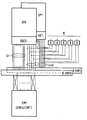
- the figure shows a section of a multiprocessor central control unit, in which e.g. Work twelve processors CP via the bus system B: CMY with the main memory CMY.
- the bus system B CMY doubled
- cf. B CMYO / B: CMY1
- possibly also the receiver unit CMY i.e. the central memory CMY, cf. CMYO / CMY1, whose two twin parts can be reached for each of the processors CP and bus systems B: CMY, cf. the line crossings.
- the processors CP which are preferably essentially identical to one another, perform, at least if there are sufficient connection requirements, simultaneous or quasi-simultaneous functions relating to switching, security and / or operation.
- Each processor can also contain its own processor-specific local memory in order to be temporarily independent of the central memory CMY, e.g. for a few data and program steps that he is currently processing or executing, and e.g. generally for frequently used program sections.
- the example shown is therefore a test device for error detection of the double circuits or processors CP of the central control unit of a telephone switching system that operate in parallel and supply binary signals.
- the test device contains, in each case a multiplicity of, parity networks per processor CP which generate test bits from the binary signals of the processors CP, namely in the EDC circuits EDCO, EDC1 of the pro
- the central memory CMY receives the binary signals and the test bits via the bus system B: CMY, cf. the special application example for test bit-secured memory addressing in the aforementioned DE-OS 33 19 710.
- the test device shown also contains a number of, here five, comparator devices VE which check bit-by-bit the identity of test bits on the relevant mutually corresponding output lines Ledc of both processors CP.
- comparator devices VE formed by AND elements for bitwise checking of the EDC code of both EDC- Circuits EDCO, EDC1 connected, but no longer for bit-wise checking of the binary signals of both processors CP.
- test bits are such a reliable image of the binary signal that even simple errors can be corrected automatically, which is why the test device structure according to the invention, despite its mostly considerable savings in hardware, is completely sufficiently reliable in a large number of applications, such as in telephone switching systems in order to recognize errors in the binary signals of one of the two circuits / processors CP immediately, that is, for example to be able to initiate the test programs for these circuits and / or e.g. in order to be able to completely switch off these circuits CP from the bus system B: CMY.
- the comparator circuits VE are connected to the output lines Ledc between the EDC circuits EDCO, EDC1 and the bus system B: CMY, the bus system B: CMY can even be disconnected particularly quickly; in principle even before it is used to initiate the acknowledgment or There is no acknowledgment of the receipt of the binary signals and the check bits.
Landscapes
- Engineering & Computer Science (AREA)
- Theoretical Computer Science (AREA)
- Computer Networks & Wireless Communication (AREA)
- Quality & Reliability (AREA)
- Physics & Mathematics (AREA)
- General Engineering & Computer Science (AREA)
- General Physics & Mathematics (AREA)
- Monitoring And Testing Of Exchanges (AREA)
- Hardware Redundancy (AREA)
- Detection And Correction Of Errors (AREA)
- Multi Processors (AREA)
Abstract
Description
Die Erfindung geht von der im Oberbegriff des Patentanspruchs 1 genannten Prüfeinrichtung aus. Die Erfindung wurde insbesondere zur Steuerung der Abschaltung eines fehlerbehafteten Prozessorpaares und Ersatz durch ein anderes Prozessorpaar in einer Multiprozessor-Zentralsteuereinheit eines Fernsprech-Vermittlungssystems nach Art der nicht vorveröffentlichten Patentanmeldungen ()83P 1722, source 83P 1724 bis 1727)The invention is based on the test device mentioned in the preamble of
entwickelt. Die Erfindung eignet sich aber für die im Oberbegriff des Patentanspruchs 1 definierten gedoppelten Schaltungen schlechthin.developed. The invention is, however, absolutely suitable for the double circuits defined in the preamble of
Die Aufgabe der Erfindung ist, die im Oberbegriff des Patentanspruchs 1 angegebenen Prüfeinrichtung so weiterzubilden, daß
- - einerseits der Hardwareaufwand gering ist und
- - andererseits die Sicherheit bzw. Zuverlässigkeit der Erkennung eines Fehlers sehr hoch ist, wobei im Prinzip sogar Einfachfehler nachträglich korrigierbar und die so korrigierten Daten nachträglich nochmals in der Prüfeinrichtung bei Bedarf auf Fehler geprüft werden können.
- - On the one hand, the hardware expenditure is low and
- - On the other hand, the security or reliability of the detection of an error is very high, in principle even simple errors can be subsequently corrected and the data corrected in this way can subsequently be checked again in the test facility for errors if necessary.
Diese Aufgabe wird durch die im Patentanspruch 1 genannten Maßnahmen gelöst.This object is achieved by the measures mentioned in
Die in dem Patentanspruch 2 angegebenen zusätzlichen Maßnahmen gestatten, zusätzlich in einem Multiprozessor-Rechner besonders einfach ein fehlerbehaftetes Prozessorpaar vom Bussystem, mit im Vergleich zur erreichten Zuverlässigkeit geringem Aufwand, abtrennen zu können.The additional measures specified in claim 2 allow a faulty processor in a multiprocessor computer in a particularly simple manner to be able to disconnect a few from the bus system with little effort compared to the reliability achieved.
Die Erfindung wird anhand von einem Ausführungsbeispiel näher erläuterte welches in der Figur gezeigt ist.The invention is explained in more detail by means of an embodiment which is shown in the figure.
Die Figur zeigt einen Ausschnitt aus einer Multiprozessor-Zentralsteuereinheit, bei der z.B. zwölf Prozessoren CP über das Bussystem B:CMY mit dem Hauptspeicher CMY zusammenarbeiten. Aus Sicherheitsgründen ist nicht nur der Prozessor CPO, vgl. COP/CP1, sondern auch das Bussystem B:CMY gedoppelt, vgl. B:CMYO/B:CMY1, evtl. auch die Empfängereinheit CMY, d.h. der zentrale Speicher CMY, vgl. CMYO/CMY1,dessen beide Zwillingsteile für jeden der Prozessoren CP und Bussysteme B:CMY erreichbar sind,vgl. die Leitungsauskreuzungen. Die - bevorzugt im wesentlichen untereinander gleichaufgebauten - Prozessoren CP führen, zumindest wenn genügend Verbindungsanforderungen vorliegen, simultan bzw. quasisimultan jeweils vermittlungstechnische, sicherungstechnische und/ oder betriebstechnische Funktionen aus. Jeder Prozessor kann dazu auch noch einen eigenen prozessorindividuellen lokalen Speicher enthalten, um zeitweise unabhängig vom zentralen Speicher CMY zu sein, z.B. für einige wenige Daten und Programmschritte, die er derzeit verarbeitet bzw. durchführt, und z.B. generell für häufig benutzte Programmabschnitte.The figure shows a section of a multiprocessor central control unit, in which e.g. Work twelve processors CP via the bus system B: CMY with the main memory CMY. For security reasons, not only the processor is CPO, cf. COP / CP1, but also the bus system B: CMY doubled, cf. B: CMYO / B: CMY1, possibly also the receiver unit CMY, i.e. the central memory CMY, cf. CMYO / CMY1, whose two twin parts can be reached for each of the processors CP and bus systems B: CMY, cf. the line crossings. The processors CP, which are preferably essentially identical to one another, perform, at least if there are sufficient connection requirements, simultaneous or quasi-simultaneous functions relating to switching, security and / or operation. Each processor can also contain its own processor-specific local memory in order to be temporarily independent of the central memory CMY, e.g. for a few data and program steps that he is currently processing or executing, and e.g. generally for frequently used program sections.
Es handelt sich also beim gezeigten Beispiel um eine Prüfeinrichtung zur Fehlererkennung der gedoppelten, parallel betriebenen und Binärsignale liefernden Schaltungen bzw. Prozessoren CP der Zentralsteuereinheit eines Fernsprech-Vermittlungssystems. Die Prüfeinrichtung enthält, jeweils eine Vielzahl von,Prüfbits aus den Binärsignalen der Prozessoren CP erzeugenden,Paritätsnetzwerke pro Prozessor CP,nämlich in den EDC-Schaltungen EDCO,EDC1 der Pro-The example shown is therefore a test device for error detection of the double circuits or processors CP of the central control unit of a telephone switching system that operate in parallel and supply binary signals. The test device contains, in each case a multiplicity of, parity networks per processor CP which generate test bits from the binary signals of the processors CP, namely in the EDC circuits EDCO, EDC1 of the pro
zessoren CP(Error Detection and Correction-Schaltungen, vgl. z.B. die käuflichen Bausteine Am 2960 und die nicht vorveröffentlichte DE-OS 33 19 710),wobei die die Binärsignale liefernden Leitungen der Prozessoren CP jeweils mit den Eingängen der EDC-Schaltungen EDCO, EDC1 verbunden sind. Beide EDC-Schaltungen EDCO, EDC1 erzeugen mittels ihrer Paritätsnetzwerke jeweils einen EDC-Code als Prüfbits der Binärsignale der mit ihnen verbundenen Prozessoren CP.cessors CP (E rr or detection and correction circuits, cf. for example the commercially available modules Am 2960 and the unpublished DE-OS 33 19 710), the lines of the processors CP providing the binary signals each having the inputs of the EDC circuits EDCO , EDC1 are connected. Both EDC circuits EDCO, EDC1 use their parity networks to generate an EDC code as test bits of the binary signals of the processors CP connected to them.
Es gibt zweierlei vieladrige Ausgangsleitungen Li, Ledc der EDC-Schaltungen bzw:der Prozessoren, nämlich Ausgangsleitungen Li für die Binärsignale, also für die von den Prozessoren CP gelieferten Ausgangsinformationen und/ oder Adressen für den zentralen Speicher CMY, sowie Ausgangsleitungen Ledc für die Prüfbits der EDC-Schaltungen EDCO/EDC1 der Prozessoren CP. Der zentrale Speicher CMY erhält über das Bussystem B:CMY die Binärsignale und die Prüfbits, vgl. das spezielle Anwendungsbeispiel für prüfbitgesicherte Speicheradressierungen in der bereits erwähnten DE-OS 33 19 710.There are two types of multi-core output lines Li, Ledc of the EDC circuits or: the processors, namely output lines Li for the binary signals, i.e. for the output information and / or addresses supplied by the processors CP and / or addresses for the central memory CMY, and output lines Ledc for the test bits of the EDC circuits EDCO / EDC1 of the processors CP. The central memory CMY receives the binary signals and the test bits via the bus system B: CMY, cf. the special application example for test bit-secured memory addressing in the aforementioned DE-OS 33 19 710.
Die gezeigte Prüfeinrichtung enthält ferner etliche, hier fünf,Vergleichereinrichtungen VE, welche bitweise die Identität von Prüfbits auf den betreffenden, einander entsprechenden Ausgangsleitungen Ledc beider Prozessoren CP überprüfen. Hierbei sind aber nur die Ausgangsleitungen Ledc für die Prüfbits beider EDC-Schaltungen EDCO, EDC1, aber nicht mehr die die Ausgangsbits weiterleitenden Ausgangsleitungen Li für die Binärsignale, mit den durch UND-Glieder gebildeten Vergleichereinrichtungen VE zur bitweisen Überprüfung des EDC-Code beider EDC-Schaltungen EDCO, EDC1 verbunden, aber nicht mehr zur bitweisen Überprüfung der Binärsignale beider Prozessoren CP.The test device shown also contains a number of, here five, comparator devices VE which check bit-by-bit the identity of test bits on the relevant mutually corresponding output lines Ledc of both processors CP. Here, however, only the output lines Ledc for the test bits of both EDC circuits EDCO, EDC1, but no longer the output lines Li forwarding the output bits for the binary signals, with the comparator devices VE formed by AND elements for bitwise checking of the EDC code of both EDC- Circuits EDCO, EDC1 connected, but no longer for bit-wise checking of the binary signals of both processors CP.
Dies bedeutet eine wesentliche Einsparung von Hardware für die Vergleichereinrichtungen VE, im Vergleich zu einer bitweisen Überprüfung des gesamten Binärsignals, erst recht zu einer bitweisen Überprüfung sowohl des gesamten Binärsignals als auch sämtlicher Prüfbits. Die Prüfbits sind ein so zuverlässiges Abbild des Binärsignals, daß sogar Einfachfehler automatisch korrigierbar sind.Daher ist der erfindungsgemäße Aufbau der Prüfeinrichtung, trotz seiner meistens sehr beachtlichen Einsparung von Hardware, in einer hohen Vielzahl von Anwendungsfällen - wie in Fernsprech-Vermittlungssystemen - völlig ausreichend zuverlässig, um Fehler in den Binärsignalen eines der beiden Schaltungen/Prozessoren CP sofort zu erkennen, also um z.B. die Testprogramme für diese Schaltungen anstoßen zu können und/oder z.B. um diese Schaltungen CP ganz vom Bussystem B:CMY abschalten zu können. Besonders falls vorsorglich die Vergleicherschaltungen VE an die Ausgangsleitungen Ledc zwischen den EDC-Schaltungen EDCO, EDC1 und dem Bussystem B:CMY angeschlossen sind, kann das Bussystem B:CMY sogar besonders rasch abgetrennt werden;-im Prinzip sogar bevor es zur Einleitung der Quittierung bzw. Nichtquittierung des Empfangs der Binärsignale und der Prüfbits kommt.This means a substantial saving in hardware for the comparator devices VE, in comparison to a bit-wise check of the entire binary signal, especially for a bit-wise check of both the entire binary signal and all check bits. The test bits are such a reliable image of the binary signal that even simple errors can be corrected automatically, which is why the test device structure according to the invention, despite its mostly considerable savings in hardware, is completely sufficiently reliable in a large number of applications, such as in telephone switching systems in order to recognize errors in the binary signals of one of the two circuits / processors CP immediately, that is, for example to be able to initiate the test programs for these circuits and / or e.g. in order to be able to completely switch off these circuits CP from the bus system B: CMY. Especially if, as a precaution, the comparator circuits VE are connected to the output lines Ledc between the EDC circuits EDCO, EDC1 and the bus system B: CMY, the bus system B: CMY can even be disconnected particularly quickly; in principle even before it is used to initiate the acknowledgment or There is no acknowledgment of the receipt of the binary signals and the check bits.
Claims (2)
Applications Claiming Priority (2)
| Application Number | Priority Date | Filing Date | Title |
|---|---|---|---|
| DE19833334765 DE3334765A1 (en) | 1983-09-26 | 1983-09-26 | TEST DEVICE FOR DETECTING ERRORS IN DOUBLE CIRCUITS, IN PARTICULAR PROCESSORS OF A TELEPHONE SWITCHING SYSTEM |
| DE3334765 | 1983-09-26 |
Publications (2)
| Publication Number | Publication Date |
|---|---|
| EP0140155A2 true EP0140155A2 (en) | 1985-05-08 |
| EP0140155A3 EP0140155A3 (en) | 1988-02-10 |
Family
ID=6210074
Family Applications (1)
| Application Number | Title | Priority Date | Filing Date |
|---|---|---|---|
| EP84111432A Ceased EP0140155A3 (en) | 1983-09-26 | 1984-09-25 | Test device for error detection in redundant circuits, especially in the control processors of a telephone switching system |
Country Status (5)
| Country | Link |
|---|---|
| EP (1) | EP0140155A3 (en) |
| JP (1) | JPS6093558A (en) |
| DE (1) | DE3334765A1 (en) |
| FI (1) | FI843755L (en) |
| ZA (1) | ZA847564B (en) |
Cited By (2)
| Publication number | Priority date | Publication date | Assignee | Title |
|---|---|---|---|---|
| DE3629399A1 (en) * | 1986-08-29 | 1988-03-03 | Siemens Ag | Method for operating the central memory of a multiprocessor-type common control unit of a switching system |
| DE10131920A1 (en) * | 2001-07-02 | 2003-01-23 | Tenovis Gmbh & Co Kg | Communication installation with distributed control, has each equipment module provided with emergency operation-control unit for switching to emergency operation mode |
Families Citing this family (4)
| Publication number | Priority date | Publication date | Assignee | Title |
|---|---|---|---|---|
| DE3334765A1 (en) * | 1983-09-26 | 1985-04-11 | Siemens AG, 1000 Berlin und 8000 München | TEST DEVICE FOR DETECTING ERRORS IN DOUBLE CIRCUITS, IN PARTICULAR PROCESSORS OF A TELEPHONE SWITCHING SYSTEM |
| US4816990A (en) * | 1986-11-05 | 1989-03-28 | Stratus Computer, Inc. | Method and apparatus for fault-tolerant computer system having expandable processor section |
| SE463900B (en) * | 1989-06-16 | 1991-02-04 | Ericsson Telefon Ab L M | PROCEDURE AND DEVICE AT A MULTIPLE PLAN UNIT IN A DIGITAL TIMER SELECTOR TO DETECT AND LOCATE ERRORS |
| US5280487A (en) * | 1989-06-16 | 1994-01-18 | Telefonaktiebolaget L M Ericsson | Method and arrangement for detecting and localizing errors or faults in a multi-plane unit incorporated in a digital time switch |
Citations (4)
| Publication number | Priority date | Publication date | Assignee | Title |
|---|---|---|---|---|
| US3982111A (en) * | 1975-08-04 | 1976-09-21 | Bell Telephone Laboratories, Incorporated | Memory diagnostic arrangement |
| US4020459A (en) * | 1975-10-28 | 1977-04-26 | Bell Telephone Laboratories, Incorporated | Parity generation and bus matching arrangement for synchronized duplicated data processing units |
| JPS56124956A (en) * | 1980-03-06 | 1981-09-30 | Nec Corp | Double information processing equipment |
| DE3334765A1 (en) * | 1983-09-26 | 1985-04-11 | Siemens AG, 1000 Berlin und 8000 München | TEST DEVICE FOR DETECTING ERRORS IN DOUBLE CIRCUITS, IN PARTICULAR PROCESSORS OF A TELEPHONE SWITCHING SYSTEM |
Family Cites Families (2)
| Publication number | Priority date | Publication date | Assignee | Title |
|---|---|---|---|---|
| IT1209187B (en) * | 1980-02-11 | 1989-07-16 | Sits Soc It Telecom Siemens | CONTROL DEVICE FOR THE CORRECT OPERATION OF A COUPLE OF PROCESSORS OPERATING ONE AS THE HOT RESERVE OF THE OTHER. |
| IT8024701A0 (en) * | 1980-09-17 | 1980-09-17 | Italtel Spa | CIRCUIT ARRANGEMENT SUITABLE FOR DETECTING THE PRESENCE OF MALFUNCTIONS IN A DATA PROCESSING SYSTEM USING A COMMERCIAL TYPE MICROPROCESSOR. |
-
1983
- 1983-09-26 DE DE19833334765 patent/DE3334765A1/en not_active Withdrawn
-
1984
- 1984-09-20 JP JP59195893A patent/JPS6093558A/en active Pending
- 1984-09-25 EP EP84111432A patent/EP0140155A3/en not_active Ceased
- 1984-09-25 FI FI843755A patent/FI843755L/en not_active Application Discontinuation
- 1984-09-26 ZA ZA847564A patent/ZA847564B/en unknown
Patent Citations (4)
| Publication number | Priority date | Publication date | Assignee | Title |
|---|---|---|---|---|
| US3982111A (en) * | 1975-08-04 | 1976-09-21 | Bell Telephone Laboratories, Incorporated | Memory diagnostic arrangement |
| US4020459A (en) * | 1975-10-28 | 1977-04-26 | Bell Telephone Laboratories, Incorporated | Parity generation and bus matching arrangement for synchronized duplicated data processing units |
| JPS56124956A (en) * | 1980-03-06 | 1981-09-30 | Nec Corp | Double information processing equipment |
| DE3334765A1 (en) * | 1983-09-26 | 1985-04-11 | Siemens AG, 1000 Berlin und 8000 München | TEST DEVICE FOR DETECTING ERRORS IN DOUBLE CIRCUITS, IN PARTICULAR PROCESSORS OF A TELEPHONE SWITCHING SYSTEM |
Non-Patent Citations (1)
| Title |
|---|
| PATENT ABSTRACTS OF JAPAN, Band 5, Nr. 202 (P-95)[874], 22. Dezember 1981; & JP-A-56 124 956 (NIPPON DENKI K.K.) 30-09-1981 * |
Cited By (2)
| Publication number | Priority date | Publication date | Assignee | Title |
|---|---|---|---|---|
| DE3629399A1 (en) * | 1986-08-29 | 1988-03-03 | Siemens Ag | Method for operating the central memory of a multiprocessor-type common control unit of a switching system |
| DE10131920A1 (en) * | 2001-07-02 | 2003-01-23 | Tenovis Gmbh & Co Kg | Communication installation with distributed control, has each equipment module provided with emergency operation-control unit for switching to emergency operation mode |
Also Published As
| Publication number | Publication date |
|---|---|
| ZA847564B (en) | 1985-05-29 |
| DE3334765A1 (en) | 1985-04-11 |
| EP0140155A3 (en) | 1988-02-10 |
| JPS6093558A (en) | 1985-05-25 |
| FI843755L (en) | 1985-03-27 |
| FI843755A0 (en) | 1984-09-25 |
Similar Documents
| Publication | Publication Date | Title |
|---|---|---|
| EP0238841B1 (en) | Error-protected multiprocessor controller having a high availability to a switching system, and method for memory configuration operation of this centraller | |
| EP1352326B1 (en) | Method and device for monitoring a data processing and transmission | |
| DE3486148T2 (en) | Fault-tolerant transmission control system. | |
| DE3787393T2 (en) | Multi-address communication method. | |
| DE3689689T2 (en) | Highly reliable computer system. | |
| DE3122076C2 (en) | ||
| DE69613056T2 (en) | Interface device between a computer of redundant architecture and a means of communication | |
| DE2202231A1 (en) | PROCESSING SYSTEM WITH TRIPLE SYSTEM UNITS | |
| DE2258917A1 (en) | CONTROL DEVICE | |
| DE2813418A1 (en) | SETUP IN AN ELECTRONIC DATA PROCESSING SYSTEM FOR REPORTING ERROR AND OPERATING CONDITIONS | |
| EP0219917B1 (en) | Switching device with fault correction | |
| DE69317507T2 (en) | Fault-tolerant computer system with a fault detector provided in each processor module | |
| DE69625953T2 (en) | Method and device for achieving high integrity and availability in a multi-channel system | |
| DE19831720A1 (en) | Method for determining a uniform global view of the system status of a distributed computer network | |
| DE69508034T2 (en) | Fault detection system and method for mirrored storage between double disk storage controllers | |
| EP0140155A2 (en) | Test device for error detection in redundant circuits, especially in the control processors of a telephone switching system | |
| DE3801123A1 (en) | MEDIATION SYSTEM | |
| DE19983975B3 (en) | Programmable control system and reset control method for the programmable control system | |
| DE69534316T2 (en) | TELECOMMUNICATION SYSTEM WITH A PROCESSOR SYSTEM AND A PROCESSOR SYSTEM | |
| EP0182134A2 (en) | Method for operating a fail-safe multi-computer system with some not fail-safe input/output units | |
| DE10084752T5 (en) | Procedure for monitoring parallel processes | |
| EP1366416A1 (en) | Fault-tolerant computer cluster and a method for operating a cluster of this type | |
| DE19619886C2 (en) | Control and data transmission system with partially redundant bus system | |
| EP0271807A2 (en) | Fault-tolerant computing system and method for detecting, localising and eliminating failing units in such a system | |
| EP3971662B1 (en) | Method for operating a redundant automation system |
Legal Events
| Date | Code | Title | Description |
|---|---|---|---|
| PUAI | Public reference made under article 153(3) epc to a published international application that has entered the european phase |
Free format text: ORIGINAL CODE: 0009012 |
|
| AK | Designated contracting states |
Designated state(s): AT BE CH DE FR GB IT LI NL SE |
|
| PUAL | Search report despatched |
Free format text: ORIGINAL CODE: 0009013 |
|
| RHK1 | Main classification (correction) |
Ipc: H04Q 3/545 |
|
| AK | Designated contracting states |
Kind code of ref document: A3 Designated state(s): AT BE CH DE FR GB IT LI NL SE |
|
| 17P | Request for examination filed |
Effective date: 19880627 |
|
| 17Q | First examination report despatched |
Effective date: 19890703 |
|
| STAA | Information on the status of an ep patent application or granted ep patent |
Free format text: STATUS: THE APPLICATION HAS BEEN REFUSED |
|
| 18R | Application refused |
Effective date: 19900816 |
|
| APAF | Appeal reference modified |
Free format text: ORIGINAL CODE: EPIDOSCREFNE |
|
| RIN1 | Information on inventor provided before grant (corrected) |
Inventor name: HUMML, SIEGFRIED Inventor name: ENGL, WALTER, DIPL.-ING. Inventor name: SCHREIER, KLAUS, DIPL.-ING. Inventor name: BITZINGER, RUDOLF, DIPL.-ING. |