EP0134960A1 - Circuit arrangement for driving a semiconductor laser - Google Patents
Circuit arrangement for driving a semiconductor laser Download PDFInfo
- Publication number
- EP0134960A1 EP0134960A1 EP84107736A EP84107736A EP0134960A1 EP 0134960 A1 EP0134960 A1 EP 0134960A1 EP 84107736 A EP84107736 A EP 84107736A EP 84107736 A EP84107736 A EP 84107736A EP 0134960 A1 EP0134960 A1 EP 0134960A1
- Authority
- EP
- European Patent Office
- Prior art keywords
- laser
- transistor
- circuit arrangement
- arrangement according
- resistor
- Prior art date
- Legal status (The legal status is an assumption and is not a legal conclusion. Google has not performed a legal analysis and makes no representation as to the accuracy of the status listed.)
- Granted
Links
- 239000004065 semiconductor Substances 0.000 title claims abstract description 9
- 230000005855 radiation Effects 0.000 claims abstract description 20
- 230000003287 optical effect Effects 0.000 claims abstract description 8
- 230000033228 biological regulation Effects 0.000 claims abstract description 3
- 230000001681 protective effect Effects 0.000 claims description 2
- 239000003990 capacitor Substances 0.000 claims 1
- 238000005259 measurement Methods 0.000 claims 1
- 230000008878 coupling Effects 0.000 abstract description 2
- 238000010168 coupling process Methods 0.000 abstract description 2
- 238000005859 coupling reaction Methods 0.000 abstract description 2
- 230000032683 aging Effects 0.000 description 1
- 230000001419 dependent effect Effects 0.000 description 1
- 230000035945 sensitivity Effects 0.000 description 1
- 230000006641 stabilisation Effects 0.000 description 1
- 238000011105 stabilization Methods 0.000 description 1
Images


Classifications
-
- H—ELECTRICITY
- H01—ELECTRIC ELEMENTS
- H01S—DEVICES USING THE PROCESS OF LIGHT AMPLIFICATION BY STIMULATED EMISSION OF RADIATION [LASER] TO AMPLIFY OR GENERATE LIGHT; DEVICES USING STIMULATED EMISSION OF ELECTROMAGNETIC RADIATION IN WAVE RANGES OTHER THAN OPTICAL
- H01S5/00—Semiconductor lasers
- H01S5/06—Arrangements for controlling the laser output parameters, e.g. by operating on the active medium
- H01S5/068—Stabilisation of laser output parameters
- H01S5/0683—Stabilisation of laser output parameters by monitoring the optical output parameters
- H01S5/06832—Stabilising during amplitude modulation
-
- H—ELECTRICITY
- H01—ELECTRIC ELEMENTS
- H01S—DEVICES USING THE PROCESS OF LIGHT AMPLIFICATION BY STIMULATED EMISSION OF RADIATION [LASER] TO AMPLIFY OR GENERATE LIGHT; DEVICES USING STIMULATED EMISSION OF ELECTROMAGNETIC RADIATION IN WAVE RANGES OTHER THAN OPTICAL
- H01S5/00—Semiconductor lasers
- H01S5/06—Arrangements for controlling the laser output parameters, e.g. by operating on the active medium
- H01S5/068—Stabilisation of laser output parameters
- H01S5/0683—Stabilisation of laser output parameters by monitoring the optical output parameters
-
- H—ELECTRICITY
- H01—ELECTRIC ELEMENTS
- H01S—DEVICES USING THE PROCESS OF LIGHT AMPLIFICATION BY STIMULATED EMISSION OF RADIATION [LASER] TO AMPLIFY OR GENERATE LIGHT; DEVICES USING STIMULATED EMISSION OF ELECTROMAGNETIC RADIATION IN WAVE RANGES OTHER THAN OPTICAL
- H01S5/00—Semiconductor lasers
- H01S5/04—Processes or apparatus for excitation, e.g. pumping, e.g. by electron beams
- H01S5/042—Electrical excitation ; Circuits therefor
Abstract
Eine Schaltanordnung zur Ansteuerung von Halbleiter-Lasern mit Regelung der gesendeten optischen Leistung unter Verwendung einer mit der Laser-Strahlung optisch gekoppelten Fotodiode, deren verstärkter Fotostrom des Strom des Lasers so steuert, daß dessen Strahlungsleistung konstant bleibt, soll insbesondere dahigehend verbessert werden, daß der Schaltungsaufwand gering, die Bandbreite groß und der Arbeitspunkt des Lasers einfach einstellbar sind, und daß darüber hinaus eine problemlose Ankopplung eines digitalen oder HF-Signals für die Modulation der Laser-Strahlung ermöglicht wird.A switching arrangement for controlling semiconductor lasers with regulation of the transmitted optical power using a photodiode which is optically coupled to the laser radiation and whose amplified photocurrent controls the current of the laser in such a way that its radiation power remains constant should be improved in particular in that the Little circuitry required, the bandwidth is large and the operating point of the laser can be easily adjusted, and in addition a problem-free coupling of a digital or RF signal for the modulation of the laser radiation is made possible.
Description
Moderne Halbleiter-Laser sind als Strahlungs-Quellen im CW-Betrieb bis zu hohen Modulations-Frequenzen (einige GHz) geeignet.Modern semiconductor lasers are suitable as radiation sources in CW operation up to high modulation frequencies (a few GHz).
CW-Halbleiter-Laser werden so betrieben, daß in der Strom-Strahlungsleistungs-Kennlinie des Lasers, vorzugsweise oberhalb des Schwellenstromes Ith, durch einen Uorstrom IF ein bestimmter DC-Arbeitspunkt eingestellt wird. Darauf wird dann auf Bedarf ein digitales oder HF-Signal moduliert, oder der Laser wird einfach als DC-Strahlungsquelle verwendet. In jedem Fall ist es aus verschiedenen Gründen (Alterung, Temperaturabhängigkeit usw.) nötig, die optische Leistung des Lasers konstant zu halten bzw. zu stabilisieren.CW semiconductor lasers are operated in such a way that a specific DC operating point is set in the current-radiation power characteristic curve of the laser, preferably above the threshold current Ith, by a pre-current I F. A digital or RF signal is then modulated on demand, or the laser is simply used as a DC radiation source. In any case, it is necessary for various reasons (aging, temperature dependency, etc.) to keep or stabilize the optical power of the laser.
Für die Stabilisierung wird vorwiegend eine mit der Laser-Strahlung optisch gekoppelte Photodiode verwendet, die meist mit dem Laser-Chip auf dem gleichen Träger aufgebaut ist. Der Photostrom der Photodiode steuert dann verstärkt über eine Regelschaltung den Strom IF des Lasers so, daß die Strahlungsleistung konstant bleibt.For stabilization, a photodiode optically coupled with the laser radiation is mainly used, which is usually constructed on the same carrier with the laser chip. The photocurrent of the photodiode then controls the current I F of the laser via a control circuit so that the radiation power remains constant.
Der Erfindung liegt die Aufgabe zugrunde, eine Schaltungsanordnung zur Ansteuerung von Halbleiter-Lasern mit Regelung der gesendeten optischen Leistung unter Verwendung einer mit der Laser-Strahlung optisch gekoppelten Photodiode dahingehend zu verbessern, daß der Schaltungsaufwand sehr gering, die Bandbreite groß und der Arbeitspunkt des Lasers einfach einstellbar sind, und daß die Schaltungsanordnung des weiteren grundsätzlich nur eine Versorgungsspannung erforderlich macht sowie eine einfache Ankopplung eines digitalen oder HF-Signals für die Modulation der Laser-Strahlung ermöglicht.The invention has for its object to improve a circuit arrangement for controlling semiconductor lasers with regulation of the transmitted optical power using a photodiode optically coupled to the laser radiation in such a way that the circuit complexity is very low, the bandwidth large and the operating point of the laser are easily adjustable, and that the circuit arrangement furthermore basically only requires a supply voltage and enables a simple coupling of a digital or RF signal for the modulation of the laser radiation.
Diese Aufgabe ist erfindungsgemäß dadurch gelost, daß die Photodiode als Signalquelle auf einen aus(wenigstens) zwei Transistoren gebildeten Transimpedanzverstärker arbeitet, dessen Ausgangsstrom zugleich der Steuerstrom des Halbleiter-Lasers ist.This object is achieved in that the photodiode works as a signal source on a transimpedance amplifier formed from (at least) two transistors, the output current of which is also the control current of the semiconductor laser.
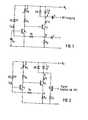
Die Erfindung wird im nachstehenden anhand einiger Schaltungsbeispiele erläutert.The invention is explained below using some circuit examples.
- Es zeigen: Fig.1 eine Laser-Ansteuerung in der erfindungsgemäßen Grundform,1 shows a laser control in the basic form according to the invention,
- Fig.2 eine hinsichtlich der Modulation der Laser-Strahlung durch Verwendung eines zusätzlichen Transistors modifizierte Schaltungsanordnung,2 shows a circuit arrangement modified with regard to the modulation of the laser radiation by using an additional transistor,
- Fig.3 eine Schaltungsanordnung mit Einstellung des Arbeitspunktes des Lasers mit Hilfe einer Referenzspannung und mit einem zusätzlichen Transistor zur Modulation der Laser-Strahlung mit einem digitalen oder HF-Signal,3 shows a circuit arrangement with adjustment of the operating point of the laser with the aid of a reference voltage and with an additional transistor for modulating the laser radiation with a digital or RF signal,
- Fig.4 eine Variante der Grundschaltung gemäß Fig. 1 mit einem zusätzlichen Transistor, der mit dem ersten Transistor des Transimpedanzverstärkers eine Stromspiegelschaltung bildet,4 shows a variant of the basic circuit according to FIG. 1 with an additional transistor which forms a current mirror circuit with the first transistor of the transimpedance amplifier,
- Fig.5 eine modifizierte Schaltungsanordnung, bei der die in der Schaltung nach Fig.1 vorgesehenen, den Laserstrom bestimmenden Widerstände durch eine aus zwei Transistoren gebildete Stromspiegelschaltung ersetzt sind.5 shows a modified circuit arrangement in which the resistors which determine the laser current and are provided in the circuit according to FIG. 1 are replaced by a current mirror circuit formed from two transistors.
In Fig.1 ist die Laser-Ansteuerschaltung in der Grundform dargestellt. Sie besteht aus den beiden Transistoren Q1,Q2, der Photodiode FD und vier Widerständen RE,RF,RO u d RV, wobei RV als Einstellwiderstand ausgebildet ist.The basic form of the laser control circuit is shown in FIG. It consists of the two transistors Q 1 , Q 2 , the photodiode FD and four resistors R E , R F , R O and R V , wherein R V is designed as an adjusting resistor.
Die Diode SD ist als Schutzdiode antiparallel zum Laser La geschaltet und hat keine weitere Funktion, außer den Laser vor negativen Spannungen zu schützen. Sie sollte deshalb eine schnelle Schaltdiode sein.The diode SD is connected as a protective diode antiparallel to the laser L a and has no other function, except to protect the laser from negative voltages. It should therefore be a fast switching diode.
Die Transistoren Q1 und Q2 bilden einen Transimpedanzverstärker mit der Photodiode FD als Signalquelle. Der Ausgangsstrom des Verstärkers, d.h. der Kollektorstrom von Q2, ist gleichzeitig der Steuerstrom IF des Halbleiter-Lasers La. Der Laserstrom IF steht somit über der Stromverstärkung Vi des Verstärkers mit dem Photostrom Ip direkt in Beziehung.The transistors Q 1 and Q 2 form a transimpedance amplifier with the photodiode FD as a signal source. The output current of the amplifier, ie the collector current of Q 2 , is also the control current I F of the semiconductor laser L a . The laser current I F is thus directly related to the photocurrent I p via the current gain V i of the amplifier.
Es gilt angenähert:

Der Photostrom Ip ist proportional zu der optischen Leistung P, die vom Laser ausgestrahlt wird:
Dabei bedeutet S die Empfindlichkeit der Photodiode.S means the sensitivity of the photodiode.
Somit ergibt sich:
Das heißt, für jede Änderung Δ P der Leistung tritt die Stromänderung Δ IF = -S.Ui.ΔP auf, die auf der Laser-Kennlinie den Arbeitspunkt so verschiebt, daß die Änderung der Leistung verkleinert wird und verschwindet.This means that for every change ΔP in power, the current change ΔI F = -SU i .ΔP occurs, which shifts the operating point on the laser characteristic curve in such a way that the change in power is reduced and disappears.
Da der Transimpedanzverstärker, der die Gegenkopplung durchführt, ein ausgesprochener Breitbandverstärker mit hoher Grenzfrequenz ist, bleibt auch die optische Gegenkopplung und Regelung bis zu sehr hohen Frequenzen wirksam.Since the transimpedance amplifier, which performs the negative feedback, is a pronounced broadband amplifier with a high cutoff frequency, the optical negative feedback and control up to very high frequencies also remain effective.
Genauer gesagt, bis zu der Grenzfrequenz fg des Verstärkers mit der Photodiode als Quelle.More specifically, up to the cut-off frequency f g of the amplifier with the photodiode as the source.
Für Frequenzen größer als die Grenzfrequenz fg der Regelstrecke wirkt die Regelung so, daß die optische Leistung auf einen bestimmten Mittelwert stabilisiert wird. Die Grenzfrequenz fg des Transimpedanzverstärkers ist bei der Verwendung von HF-Transistoren für Q1, Q2 angenähert umgekehrt proportional zu dem Produkt RF.CF 
Mit kapazitätsarmen schnellen Photodioden erreicht fg sehr hohe Werte. Andererseits ist sehr oft erwünscht, auf einen Mittelwert der optischen Leistung zu stabilisieren. In diesem Fall wird durch Zuschalten von externen Kapazitäten Ce am Eingang vom Verstärker die Grenzfrequenz auf dem gewünschten Wert herabgesetzt.With low-capacitance fast photodiodes, fg reaches very high values. On the other hand, it is very often desirable to stabilize on an average optical power. In this case, the cut-in frequency is reduced to the desired value by connecting external capacitances C e at the input of the amplifier.
Die Modulation der Lasr-Strahlung mit einem Signal kann am Punkt A oder Punkt B über eine Kapazität C erfolgen.The Lasr radiation can be modulated with a signal at point A or point B via a capacitance C.
Eine andere Möglichkeit, die Laser-Strahlung mit einem digitalen oder Hf-Signal zu modulieren, wird in Fig. 2 und Fig.3 gezeigt. Es wird hier ein zusätzlicher Transistor Q3 verwendet, der mit seinem Emitter am Punkt B, Fig.3, oder mit seinem Kollektor am Punkt A, Fig. 2, angeschlossen ist, wobei in diesem Fall der Emitter über einen Widerstand R3 am Minuspol der Speisespannungsquelle liegt. Über die Basis des Transistors Q3 kann dann in beiden Fällen der Laser La mit dem Nutzsignal moduliert werden .Another possibility of modulating the laser radiation with a digital or RF signal is shown in FIGS. 2 and 3. An additional transistor Q 3 is used here, which is connected with its emitter at point B, FIG. 3, or with its collector at point A, FIG. 2, in which case the emitter is connected to the negative pole via a resistor R 3 the supply voltage source. In both cases, the laser L a can then be modulated with the useful signal via the base of the transistor Q 3 .
Zur Modulation der Laser-Strahlung mit einem externen Signal am Punkt 8 eignet sich auch die in Fig. 5 dargestellte Schaltungsvariente. Hier wird ebenfalls ein zusätzlicher Tran- sistor Q3'verwendet, der mit dem Widerstand RB parallel zum Widerstand RE liegt. Der Transistor Q3' kann auch der Ausgang eines TTL-Gatters mit Open-Collector-Ausgängen sein.The circuit variant shown in FIG. 5 is also suitable for modulating the laser radiation with an external signal at point 8. Here, an additional transit is also istor s Q 3 'is used, which is connected to the resistor R B in parallel with resistor R E. The transistor Q 3 'can also be the output of a TTL gate with open collector outputs.
Die Beschaltung von Q3 in Fig. 3 entspricht dem Ausgang eines ECL-Gatters. Am Punkt B kann demnach der Laser direkt auch mit einem Gatter dieser schnellen Logik moduliert werden.The connection of Q 3 in Fig. 3 corresponds to the output of an ECL gate. At point B, the laser can therefore also be modulated directly with a gate of this fast logic.
Der Arbeitspunkt und der Arbeitsbereich des Lasers in der Strom-Leistungs-Kennlinie wird im Falle der Figuren 1,2 und 4 grob mit dem Widerstand RE und fein mit dem Widerstand RV eingestellt. Bei vorgegebenen Widerständen RF und RE bestimmt der Widerstand RO den maximalen Strom IFmax und die Summe RO+RVmax den minimalen Strom IFmin durch den Laser La.The working point and the working range of the laser in the current-power characteristic curve are set roughly with the resistor R E and fine with the resistor R V in the case of FIGS. With predetermined resistances R F and R E , the resistance R O determines the maximum current I Fmax and the sum R O + R Vmax determines the minimum current I Fmin through the laser L a .
Zwei weitere Möglichkeiten, den Arbeitspunkt des Lasers einzustellen, zeigen die Figuren 3 und 5. Bei der Schaltungsanordnung gemäß Fig. 3 wird der Arbeitspunkt mit Hilfe einer Re- ferenzspannung UREF an der Basis des Transistors Q3 festgelegt. In diesem Fall entfällat der Widerstand RV, so daß zwischen der Basis des ersten Transistors Q1 und dem Pluspol der Speisespannungsquelle lediglich noch der Widers stand RO liegt.Two other possibilities to adjust the operating point of the laser, shown in FIGS 3 and 5. In the circuit arrangement shown in FIG. 3 is set the operating point with the aid of a re p a retr ferenzs U REF at the base of the transistor Q 3. In this case, the resistor R V is omitted, so that between the base of the first transistor Q 1 and the positive pole of the supply voltage source, only the contradiction is R O.
Bei den Schaltungsanordnung nach Fig. 5 sind die Widerstände RV, RO durch eine Stromspiegelschaltung Q4,Q5 ersetzt. Die Feineinstellung des Arbeitspunktes geschieht hier mit dem variablen Widerstand Rp. Der Einstellwiderstand RV in Figur 1 ist hier zwischen den Minuspol und die miteinander verbundenen Kollektor-Basisanschlüsse des Transistors Q5 verlegt.In the circuit arrangement according to FIG. 5, the resistors R V , R O are replaced by a current mirror circuit Q 4 , Q 5 . The fine adjustment of the operating point is done here with the variable resistor Rp. The setting resistor R V in FIG. 1 is here laid between the negative pole and the interconnected collector base connections of the transistor Q 5 .
Der Vorteil der Schaltungsanordnung nach Fig. 5 gegenüber derjenigen gemäß Fig. 1 liegt darin, daß im Fall der Fig. 5 am Kollektor von Q1 jetzt der Kollektor von Q4 als Stromquelle angeschlossen ist. Diese Stromquelle (Kollektor von Q4) entspricht, fast unabhängig vom Strom, einem groBen Lastwiderstand für den Transistor Q1, so daß die innere Verstärkung des aus den Transistoren Q1 und Q2 bestehenden Transimpedanzverstärkers in einem weiten Streubereich groß und stabil bleibt. Damit werden auch die Eigenschaften des Transimpedanzverstärkers wenig abhängig vom eingestellten Arbeitspunkt und Strom. Die Emitter der PNP-Transistoren Q4 und Q5 sind jeweils über einen Widerstand R4 bzw. R5 mit der am Pluspol der Spannungsquelle liegenden Kathode der Photodiode FD leitend verbunden.The advantage of the circuit of Fig. 5 with respect to that of FIG. 1 is that 5 at the collector of Q 1 now the collector of Q 4 is connected as a current source in the case of FIG.. This current source (collector of Q 4 ) corresponds, almost independent of the current, to a large load resistance for the transistor Q 1 , so that the internal gain of the transimpedance amplifier consisting of the transistors Q 1 and Q 2 remains large and stable over a wide range. This means that the properties of the transimpedance amplifier are not very dependent on the set operating point and current. The emitters of the PNP transistors Q 4 and Q 5 are each conductively connected via a resistor R 4 or R 5 to the cathode of the photodiode FD located at the positive pole of the voltage source.
In Fig. 4 ist eine weitere Variante der Grundschaltung von Fig. 1 dargestellt. Es wird hier ein zusätzlicher Transistor QO verwendet, der mit dem Transistor Q1 eine Stromspiegelschaltung bildet. Q1 und Q2 sind immer noch als Transimpedanzverstärker beschaltet. Diese Schaltung hat als Vorteil eine sehr gute Temperaturstabilität, falls die Transistoren Q1 und QO miteinander thermisch gekoppelt sind.4 shows a further variant of the basic circuit of FIG. 1. An additional transistor Q O is used here, which forms a current mirror circuit with transistor Q 1 . Q 1 and Q 2 are still connected as transimpedance amplifiers. This circuit has the advantage of very good temperature stability if the transistors Q 1 and Q O are thermally coupled to one another.
Die Grenzfrequenz der Regelschaltung nach der Erfindung erreicht bei Verwendung geeigneter HF- oder UHF-Transistoren, Werte von einigen 100MHZ und ist primär nur durch die Grenzfrequenz der Photodiode FD'begrenzt. Im Bedarfsfall kann die Schaltung auch an zwei Versorgungsspannungen angeschlossen werden.The limit frequency of the control circuit according to the invention, when using suitable HF or UHF transistors, reaches values of a few 100 MHz and is primarily limited only by the limit frequency of the photodiode FD '. If necessary, the circuit can also be connected to two supply voltages.
Claims (15)
Applications Claiming Priority (2)
| Application Number | Priority Date | Filing Date | Title |
|---|---|---|---|
| DE3325420A DE3325420A1 (en) | 1983-07-14 | 1983-07-14 | CIRCUIT ARRANGEMENT FOR CONTROLLING SEMICONDUCTOR LASERS |
| DE3325420 | 1983-07-14 |
Publications (2)
| Publication Number | Publication Date |
|---|---|
| EP0134960A1 true EP0134960A1 (en) | 1985-03-27 |
| EP0134960B1 EP0134960B1 (en) | 1987-07-22 |
Family
ID=6203982
Family Applications (1)
| Application Number | Title | Priority Date | Filing Date |
|---|---|---|---|
| EP84107736A Expired EP0134960B1 (en) | 1983-07-14 | 1984-07-04 | Circuit arrangement for driving a semiconductor laser |
Country Status (3)
| Country | Link |
|---|---|
| US (1) | US4674093A (en) |
| EP (1) | EP0134960B1 (en) |
| DE (1) | DE3325420A1 (en) |
Cited By (5)
| Publication number | Priority date | Publication date | Assignee | Title |
|---|---|---|---|---|
| EP0213784A2 (en) * | 1985-08-21 | 1987-03-11 | THE GENERAL ELECTRIC COMPANY, p.l.c. | Apparatus for amplitude modulating the output of a laser diode or L.E.D. |
| EP0308058A2 (en) * | 1987-08-19 | 1989-03-22 | Plessey Overseas Limited | Power supply |
| WO1991004595A1 (en) * | 1989-09-22 | 1991-04-04 | Imatronic Limited | Laser diode supply circuit |
| WO1991015886A1 (en) * | 1990-04-03 | 1991-10-17 | Raynet Corporation | Thermal control for laser diode used in outside plant communications terminal |
| WO1992003860A1 (en) * | 1990-08-17 | 1992-03-05 | Linotype-Hell Ag | Process and circuitry for controlling a laser diode |
Families Citing this family (16)
| Publication number | Priority date | Publication date | Assignee | Title |
|---|---|---|---|---|
| US4709370A (en) * | 1985-06-17 | 1987-11-24 | Rca Corporation | Semiconductor laser driver circuit |
| DE3629349A1 (en) * | 1986-08-28 | 1988-03-10 | Theralux Lichttechnische Anlag | Triggerable pulse generator |
| JPS6381881A (en) * | 1986-09-25 | 1988-04-12 | Minolta Camera Co Ltd | Laser oscillator |
| US5036519A (en) * | 1988-12-05 | 1991-07-30 | Ricoh Company, Ltd. | Semiconductor laser controller |
| US5123023A (en) * | 1990-11-21 | 1992-06-16 | Polaroid Corporation | Laser driver with plural feedback loops |
| DE4110095C2 (en) * | 1991-03-27 | 1998-02-12 | Draegerwerk Ag | Method for gas spectroscopic measurement of the concentration of a gas component |
| US5402432A (en) * | 1993-06-01 | 1995-03-28 | Quarton, Inc. | Semi-conductor laser device constant power output controller |
| US5524015A (en) * | 1994-07-19 | 1996-06-04 | Spectra-Physics Lasers, Inc. | Optical noise reduction circuitry for laser systems |
| US5442648A (en) * | 1994-07-19 | 1995-08-15 | Spectra Physics Lasers, Inc. | Noise rejection circuitry and laser system using the same |
| JP2001505100A (en) * | 1996-11-21 | 2001-04-17 | ボストン サイエンティフィック コーポレイション | Mucosal detachment using light |
| US6444970B1 (en) | 1998-06-26 | 2002-09-03 | Scimed Life Systems, Inc. | Miniature low-noise photodiode system |
| KR100544204B1 (en) * | 2004-06-24 | 2006-01-23 | 삼성전자주식회사 | Optical output controller |
| US9312701B1 (en) | 2015-07-16 | 2016-04-12 | Wi-Charge Ltd | System for optical wireless power supply |
| EP3430738B1 (en) | 2016-03-14 | 2021-10-13 | Wi-Charge Ltd. | System for optical wireless power supply |
| KR102399819B1 (en) * | 2016-04-11 | 2022-05-18 | 위-차지 리미티드. | Systems for Optical Wireless Power Supplies |
| CN110995170B (en) * | 2019-12-25 | 2023-04-21 | 武汉邮电科学研究院有限公司 | High dynamic range transimpedance amplifier |
Citations (1)
| Publication number | Priority date | Publication date | Assignee | Title |
|---|---|---|---|---|
| GB2066557A (en) * | 1979-12-27 | 1981-07-08 | Western Electric Co | Injection laser output stabilisation |
Family Cites Families (8)
| Publication number | Priority date | Publication date | Assignee | Title |
|---|---|---|---|---|
| US3898583A (en) * | 1972-03-29 | 1975-08-05 | Xerox Corp | Laser stabilization technique |
| DE2218431C3 (en) * | 1972-04-17 | 1986-10-23 | Siemens AG, 1000 Berlin und 8000 München | Circuit arrangement to compensate for the non-linear relationship between applied voltage and light emission in luminescent diodes |
| US3909745A (en) * | 1974-10-17 | 1975-09-30 | Hughes Aircraft Co | Laser transmitter system |
| CA1062824A (en) * | 1975-02-10 | 1979-09-18 | Western Electric Company, Incorporated | Two-way telephone transmission system utilizing opto-couplers |
| US4109217A (en) * | 1976-12-10 | 1978-08-22 | Bell Telephone Laboratories, Incorporated | Stabilization circuit for junction lasers |
| DE2854000C2 (en) * | 1978-12-14 | 1982-04-01 | Fraunhofer-Gesellschaft zur Förderung der angewandten Forschung e.V., 8000 München | Circuit arrangement for a switchable constant current source for light transmitters |
| DE2911858C2 (en) * | 1979-03-26 | 1983-01-13 | Robert Bosch Gmbh, 7000 Stuttgart | Circuit for limiting the light output emitted by a semiconductor laser |
| US4339822A (en) * | 1979-08-08 | 1982-07-13 | Optical Information Systems, Inc. | Diode laser digital modulator |
-
1983
- 1983-07-14 DE DE3325420A patent/DE3325420A1/en active Granted
-
1984
- 1984-07-04 EP EP84107736A patent/EP0134960B1/en not_active Expired
- 1984-07-06 US US06/628,653 patent/US4674093A/en not_active Expired - Lifetime
Patent Citations (1)
| Publication number | Priority date | Publication date | Assignee | Title |
|---|---|---|---|---|
| GB2066557A (en) * | 1979-12-27 | 1981-07-08 | Western Electric Co | Injection laser output stabilisation |
Non-Patent Citations (2)
| Title |
|---|
| PATENTS ABSTRACTS OF JAPAN, Band 7, Nr. 204 (E-197)(1349), September 9, 1983; & JP - A - 58 100479 (OKI DENKI KOGYO K.K.) 15.06.1983 * |
| TECHNISCHES MESSEN, T.M., Band 50, Nr. 2, Februar 1983, Seiten 49-54, München, DE; W.S. LUDOLF: "Grundlagen der optischen Übertragungstechnik - Eine Einführung für Anwender" * |
Cited By (10)
| Publication number | Priority date | Publication date | Assignee | Title |
|---|---|---|---|---|
| EP0213784A2 (en) * | 1985-08-21 | 1987-03-11 | THE GENERAL ELECTRIC COMPANY, p.l.c. | Apparatus for amplitude modulating the output of a laser diode or L.E.D. |
| EP0213784A3 (en) * | 1985-08-21 | 1989-03-15 | THE GENERAL ELECTRIC COMPANY, p.l.c. | Apparatus for amplitude modulating the output of a laser diode or l.e.d. |
| EP0308058A2 (en) * | 1987-08-19 | 1989-03-22 | Plessey Overseas Limited | Power supply |
| EP0308058A3 (en) * | 1987-08-19 | 1991-04-03 | Plessey Overseas Limited | Power supply |
| WO1991004595A1 (en) * | 1989-09-22 | 1991-04-04 | Imatronic Limited | Laser diode supply circuit |
| WO1991015886A1 (en) * | 1990-04-03 | 1991-10-17 | Raynet Corporation | Thermal control for laser diode used in outside plant communications terminal |
| AU644169B2 (en) * | 1990-04-03 | 1993-12-02 | Raynet Corporation | Thermal control for laser diode used in outside plant communications terminal |
| US5319656A (en) * | 1990-04-03 | 1994-06-07 | Raynet Corporation | Thermal control for laser diode used in outside plant communications terminal |
| WO1992003860A1 (en) * | 1990-08-17 | 1992-03-05 | Linotype-Hell Ag | Process and circuitry for controlling a laser diode |
| US5303251A (en) * | 1990-08-17 | 1994-04-12 | Linotype-Hell Ag | Method and circuit arrangement for driving a laser diode |
Also Published As
| Publication number | Publication date |
|---|---|
| US4674093A (en) | 1987-06-16 |
| DE3325420A1 (en) | 1985-01-31 |
| DE3325420C2 (en) | 1989-08-10 |
| EP0134960B1 (en) | 1987-07-22 |
Similar Documents
| Publication | Publication Date | Title |
|---|---|---|
| EP0134960B1 (en) | Circuit arrangement for driving a semiconductor laser | |
| DE4225621B4 (en) | Apparatus and method for supplying a light beam of controllable intensity | |
| EP0421516B1 (en) | Power supply arrangement with voltage regulation and current limiting | |
| DE2923683A1 (en) | STABILIZING CIRCUIT OF A LASER | |
| DE2841433A1 (en) | PRE-CURRENT CONTROL OF LASER DIODES | |
| DE2653624B2 (en) | Color video signal amplifier | |
| EP1445843B1 (en) | Driver and operation method for semiconductor lasers | |
| EP0361342A2 (en) | Optical receiver with a widened dynamic range | |
| EP0169388B1 (en) | Integrated constant-current source | |
| EP0166973B1 (en) | Differential amplifier | |
| DE3317027A1 (en) | CIRCUIT ARRANGEMENT FOR CONVERTING AN ELECTRICAL INPUT SIGNAL TO AN OPTICAL OUTPUT SIGNAL | |
| DE3522416A1 (en) | Controllable broadband amplifier circuit | |
| DE3327249A1 (en) | TEMPERATURE COMPENSATING VOLTAGE CIRCUIT | |
| EP0462304B1 (en) | Arrangement for the amplitude regulation of an oscillator | |
| EP0163302A2 (en) | Drive circuit for a deflection power transistor | |
| DE2648080C3 (en) | Broadband amplifier with variable gain | |
| EP0028743A1 (en) | Circuit for generating a sine wave from a triangular wave | |
| DE4210215C2 (en) | Differential amplifier arrangement | |
| EP0792014A2 (en) | Circuit for controlling the output amplitude of a high frequency power amplifier | |
| DE1487395A1 (en) | Adjustable amplifier | |
| EP0658016B1 (en) | Optical transmitter with linearising termination network | |
| DE3902871A1 (en) | Automatic control of the operating point of radio-frequency field-effect transistors in keyed pulse mode | |
| DE2032682A1 (en) | Push-pull amplifier | |
| DE4317686C2 (en) | Current mirror circuit | |
| DE4030995A1 (en) | Laser-diode for fast data transmission with servo output - uses photodiode to monitor and set threshold and modulator currents |
Legal Events
| Date | Code | Title | Description |
|---|---|---|---|
| PUAI | Public reference made under article 153(3) epc to a published international application that has entered the european phase |
Free format text: ORIGINAL CODE: 0009012 |
|
| AK | Designated contracting states |
Designated state(s): FR GB IT NL |
|
| 17P | Request for examination filed |
Effective date: 19850813 |
|
| 17Q | First examination report despatched |
Effective date: 19860722 |
|
| GRAA | (expected) grant |
Free format text: ORIGINAL CODE: 0009210 |
|
| AK | Designated contracting states |
Kind code of ref document: B1 Designated state(s): FR GB IT NL |
|
| ET | Fr: translation filed | ||
| ITF | It: translation for a ep patent filed |
Owner name: DE DOMINICIS & MAYER S.R.L. |
|
| PLBE | No opposition filed within time limit |
Free format text: ORIGINAL CODE: 0009261 |
|
| STAA | Information on the status of an ep patent application or granted ep patent |
Free format text: STATUS: NO OPPOSITION FILED WITHIN TIME LIMIT |
|
| 26N | No opposition filed | ||
| PGFP | Annual fee paid to national office [announced via postgrant information from national office to epo] |
Ref country code: GB Payment date: 19900620 Year of fee payment: 7 |
|
| PGFP | Annual fee paid to national office [announced via postgrant information from national office to epo] |
Ref country code: FR Payment date: 19900706 Year of fee payment: 7 |
|
| ITTA | It: last paid annual fee | ||
| PGFP | Annual fee paid to national office [announced via postgrant information from national office to epo] |
Ref country code: NL Payment date: 19900731 Year of fee payment: 7 |
|
| PG25 | Lapsed in a contracting state [announced via postgrant information from national office to epo] |
Ref country code: GB Effective date: 19910704 |
|
| PG25 | Lapsed in a contracting state [announced via postgrant information from national office to epo] |
Ref country code: NL Effective date: 19920201 |
|
| GBPC | Gb: european patent ceased through non-payment of renewal fee | ||
| NLV4 | Nl: lapsed or anulled due to non-payment of the annual fee | ||
| PG25 | Lapsed in a contracting state [announced via postgrant information from national office to epo] |
Ref country code: FR Effective date: 19920331 |
|
| REG | Reference to a national code |
Ref country code: FR Ref legal event code: ST |