EP0133006A2 - Safe operation proving of electronic circuits - Google Patents
Safe operation proving of electronic circuits Download PDFInfo
- Publication number
- EP0133006A2 EP0133006A2 EP84305006A EP84305006A EP0133006A2 EP 0133006 A2 EP0133006 A2 EP 0133006A2 EP 84305006 A EP84305006 A EP 84305006A EP 84305006 A EP84305006 A EP 84305006A EP 0133006 A2 EP0133006 A2 EP 0133006A2
- Authority
- EP
- European Patent Office
- Prior art keywords
- output
- signal
- circuit
- arrangement according
- electronic circuit
- Prior art date
- Legal status (The legal status is an assumption and is not a legal conclusion. Google has not performed a legal analysis and makes no representation as to the accuracy of the status listed.)
- Withdrawn
Links
- 239000003990 capacitor Substances 0.000 claims description 19
- 230000003287 optical effect Effects 0.000 claims description 4
- 230000001934 delay Effects 0.000 abstract 1
- 238000000034 method Methods 0.000 description 5
- 238000005513 bias potential Methods 0.000 description 4
- 238000010586 diagram Methods 0.000 description 4
- 238000001514 detection method Methods 0.000 description 2
- 230000002401 inhibitory effect Effects 0.000 description 2
- 230000005540 biological transmission Effects 0.000 description 1
- 230000000903 blocking effect Effects 0.000 description 1
- 238000011156 evaluation Methods 0.000 description 1
- 238000001914 filtration Methods 0.000 description 1
- 230000011664 signaling Effects 0.000 description 1
- 238000001228 spectrum Methods 0.000 description 1
Images
Classifications
-
- B—PERFORMING OPERATIONS; TRANSPORTING
- B61—RAILWAYS
- B61L—GUIDING RAILWAY TRAFFIC; ENSURING THE SAFETY OF RAILWAY TRAFFIC
- B61L1/00—Devices along the route controlled by interaction with the vehicle or train
- B61L1/18—Railway track circuits
- B61L1/181—Details
- B61L1/188—Use of coded current
-
- H—ELECTRICITY
- H03—ELECTRONIC CIRCUITRY
- H03K—PULSE TECHNIQUE
- H03K19/00—Logic circuits, i.e. having at least two inputs acting on one output; Inverting circuits
- H03K19/007—Fail-safe circuits
Definitions
- the invention relates to proving safe operation and failure to safety of electronic circuits.
- Safe operation in the context of the present invention includes correct operation of the apparatus and also, in the event of an error being detected or a fault occuring, the automatic switching of the output of the apparatus into a safe state.
- the invention is particularly useful in systems where a decision concerning safety is based upon the output signal, so that incorrect operation of the signal processing circuits producing that signal can directly affect the safety of the system.
- a mass transit system such as an underground railway, having an automatic train protection system in which a coded signal representing safe maximum train speed is transmitted to the train for analysis by the train and comparison with a signal reresenting the train's measured speed. If the coded signal is incorrectly decoded or is corrupted before comparison then a wrong decision conerning the maximum speed at which it is safe for the train to travel may be the result.
- One receiver apparatus for an automatic train protection system of this type is described in the Applicants U.K. Patent No. 2,017,991.
- the invention may be useful in coded track circuits in which a coded signal is transmitted between a track circuit transmitter and track circuit receiver via the running rails.
- a coded signal is transmitted between a track circuit transmitter and track circuit receiver via the running rails.
- the section of rails i.e. the track section
- the rails are electrically shorted together thus preventing propagation of the signal along the section.
- the present invention may be applied to the receiver apparatus in order to verify its correct operation at all times.
- a railway track circuit receiver of this type to which the invention may be applied is described in Applicant's U.K. Patent Application No. 2,114,342.
- an arrangement for proving safe operation of an electronic circuit comprising means responsive to the presence of predetermined signal characteristics in an output of the electronic circuit to pass a correctly produced output signal, having said characteristics, to a further output or to disable an incorrectly produced signal.
- an arrangement further including means for generating a signal having said predetermined characteristics and means for superimposing said signal on an input to the electronic circuit safe operation of which is to be proved.
- a first concerning a railway automatic train protection system hereinafter referred to as an ATP system
- a second concerning a railway track circuit application especially useful for coded jointless track circuits.
- the means for sensing the characteristics i.e. the amplitude and frequency of the chosen signal
- a frequency spectrum analyser of a particular type, namely a microprocessor based system adapted to evaluate a fast or discrete Fourier transfom algorithm.
- 83 20 486 (which is concerned with proving the safe operation of a signal channel processor system such as that disclosed in GB 2,114,342) and also the technique of 83 20 514 (which is concerned with proving correction operations of electronic circuits, inter alia microprocessors) also find application in combination with the present invention.
- the above referenced applications GB 82 20 486 and GB 83 20 514 were filed concurrently with the priority application (No. 83 20 509) of this specification, and references to those applications are to be construed as including reference to any subsequent patent application claiming priority therefrom.
- each electronic processing circuit For proving safe operation of each electronic processing circuits there is provided means adapted to generate in the output of an electronic processing circuit an additional signal of predetermined characteristics, or to sense a particular signal characteristic, and a gating arrangement connected to the output including latching means wherein a gate is energised by supplementary supply voltage generated in response to detection of the additional signal.
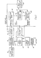
- Fig. 1 shows a block diagram of an ATP transmitter arrangement in which the transmitter circuits themselves have been omitted because they form no part of the present invention.
- the basic speed indicating code signals are generated by a code oscillator and divider circuits in block 10, one of the codes is selected by means not shown to represent a maximum safe speed limit.
- the selected coded frequency and a carrier signal from carrier generator 11 are connected to an amplitude modulation generator 12 the amplitude modulated output 13 of which is then connected via a safe enable gate 14 to a power output stage 15, and thence via an output transformer 16 to transmitter circuits (not shown).
- the safe enable gate 14 is added to the signal path by application of the invention.
- circuits for carrying out the invention are illustrated to the right of Fig. 1 and comprises an anti-alias filter 17 connected to receive the amplitude modulated signal 13 and connected to the data input of a microprocessor 18.
- the microprocessor output is connected via a processor output enable gate 19 to a proving circuit 20 the output of which controls operation of the enable gate 14.
- the proving circuit 20 is also connected to a control input 21 of enable gate 19 to provide a self-latching facility for normal operation.
- a start up circuit 22 is provided which receives an input from the carrier generator 11 and provides a signal to the control input 21 of microprocessor output enabling gate 19.
- the 3 MHz clock frequency of the microprocessor 18 is connected to the block 11 which consists basically of frequency dividing circuits.
- the illustrated arrangement does not include a separate proving signal generator, instead the amplitude modulated frequency which appears in the modulated output 13 is made to serve the same purpose.
- the arrangement of Fig. 1 utilizes output gating means in accordance with the invention on a first level to pass the output of the frequency analysing microprocessor 18, and then at a second level utilizes a further gating means 14 to pass the output from the a.m. generator 12. Also, to accommodate the cycle or processing time of the microprocessor system 18, the self start-up circuit 22 provides a time delay greater than one cycle period so that normal operation of the arrangement is established initially. If the processor system is operated in accordance with the invention of GB 83 20 486 the delay time is preferably greater than the period of two operating cycles.
- a transmitter carrier signal modulated by a selected code frequency is generated in the normal way and output signal 13 is connected through a safe enable gate 14 for transmission.
- the amplitude modulated signal 13 is also connected via a safe anti-alias filter 17 to the data input of a microprocessor 18 which is programmed to perform a digital filtering function by means of a Fast Fourier Transform technique, such a technique is more fully described in Applicant's U.K. Patent Application No. 2,114,342.
- the processor output comprises a data signal giving the amplitude levels of the components of the amplitude modulated input signal lying within a multiplicity of frequency bins.
- This output is connected via an enabling gate 19 to a processor output proving circuit 20 which verifies that the modulated signal contains one of the code frequencies, that said modulating signal has sufficient amplitude and that its frequency lies within a permitted range. Subject to these criteria being met the proving circuit 20 produces outputs one of which maintains the enable gate 14 and another which is fed back to control input 21 to maintain the enable gate 19, the latter thereby constituting a self-latching circuit.
- the start-up circuit 22 is provided with an output from the carrier signal generator and is arranged to provide an alternative and temporary latching signal to input 21 of gate 19.
- the proving circuit 20 removes the maintaining signals from gate 14 and gate 19.
- the former prevents the amplitude modulated signal reaching the power output stage 15, thereby effectively inhibiting the transmitter, and the latter effectively latches-out the proving circuit 20 preventing subsequent restoration of the maintaining signal should the fault prove only to be temporary.
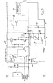
- FIG. 2 shows in greater detail a circuit diagram of part of a circuit suitable for use in the general arrangement of Fig. 1, in which the microprocessor output enable gate is enclosed by chain linked line 19, the processor output proving circuits by block 20, and the start up circuit is enclosed by another chain linked line 22.
- the latching action mentioned above which maintains enable gate 19 is carried into practice by providing 5 volts on the line indicated at reference 21.
- a signal from the carrier generator 11 (see Fig. 1) is provided at input 30 in the form of a square wave input signal.
- the voltage on the capacitor 31 is initially zero volts when the circuit is switched on, and so the transistor 32 is biased “off” allowing the square wave input signal to switch transistor 33 which drives a further push-pull arrangement of transistors 34, 35.
- This output of this arragement is connected to a diode pump circuit comprising capacitors 36, 37 and doides 38, 39 and 40, in which the anode of diode 40 and one terminal of capacitor 37 is connected to the-5 volt line 21.
- the enable gate 19 basically comprises a photo-responsive diode 41 connected in the base circuit of a transistor 42 which is connected in parallel with diode 40 and capacitor 37 between the 0 volts and -5 volt lines.
- the output of microprocessor 18 is connected through a further transistor 43 to drive a light emitting diode 44 optically coupled with the doide 41.
- a light emitting diode 44 in the collected circuit of transistor 42 is optically coupled with a photo-responsive diode 45 connected in an input stage to proving circuit 20.
- the capacitor 31 is initially discharged, upon initial energisation of the power supply to the circuits and the transmitter a square wave signal appears at input 30 and is permitted to switch transistor 33 which drives the doide pump arrangement to produce -5 volts on line 21.
- This negative voltage energises transistor 42 and permits the microprocessor output to be relayed via transistors 43, the opto-coupler comprising diodes 41, 44 and the second opto-coupler, of doides 45, 46 to the proving circuit 20.
- Gradually capacitor 31 charges up thus inhibiting input 30 from continuing to operate the doide pump circuit.
- the proving circuit 20 Upon receiving the microprocessor output the proving circuit 20 will generate a -5volts supply on line 21 providing it has satisfactorily proved the microprocessor output to be correct. Having once been charged the capacitor 31 maintains the bias on transistors 32 and 33 for as long as the normal power supply is maintained. The signal on input 30 is only again permitted to operate the doide pump circuit if the supply voltage source is de-energised and capacitor 31 allowed to discharge.
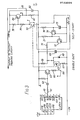
- FIG. 3 An alternative circuit for an enable gate and self-start circuit are shown in Fig. 3.
- the processor system again represented by single block 18 performs the operations of decimation and evaluation of the transform algorithm on an input waveform.
- the processor 18 is adapted to check that the amplitude modulated carrier signal comprises only one of a set of possible modulation frequencies and does not include more than one modulation frequency, these frequencies being the preselected signal characteristics. Subject to one of these frequency being sensed the processor system 18 produces an output on line 60 comprising a unipolar amplitude modulated carrier signal of 2.5 KHz modulated at 320Hz.
- the input line 60 is connected through a high pass filter comprising resistor 61 and capacitor 62 to the base terminal of a switching transistor 63.
- the collector load of this transistor in which a junction point 64 is connected to the cathode of the light emitting part 65 of an optical coupler, the collector load resistors 66 and 67 form a potential divider providing a reference potential to the LED 65.
- a further anti-parallel diode 68 is connected from the anode of the LED 65 to a negative voltage bias potential -5 volts and reservoir capacitor 69 is connected between here and a reference potential 0 volts supply.
- a further resistor 70 is connected between the common connected anode and cathode of diodes 65 and 68 respectively to the reference supply.
- This circuit section constitutes an enable gate.
- the circuit mode at the anode and cathode of doides 65 and 68 is also connected through a resistor 71 in the load current path of switching transistor arrangement comprising transistor 72, resistor 73 and transistor 74.
- the base terminal of the latter transistor is connected to the variable potential terminal of a capacitor 75 and resistor 76 connected to the reference potential.
- This circuit section constitues a self-start circuit.
- the optical coupler is completed by a light receiving transistor 77 connected in an amplifier circuit comprising potential divider 78 and 79, ampliying transistor 81, resistor 81 and capacitor 82 which provides an output at 83 connected to the output proving block 20 of Fig. 1.
- the proving circuit 20 comprising a rectifier circuit responsive to an alternating signal on line 83 to maintain a latching output signal or enable signal to the gate 14 and the self start circuit 22, see Fig. 1. This enable signal also constitutes the -5 volts supply for the enable gate, see Fig. 3.
- the capacitors 69 and 75 are initially discharged and in order for the enable gate to operate the diode 65 must be forward baised.
- the bias potential for doide 65 is obtained from the output 83, via the proving circuit 20 of Fig. 1, and therefore through a fully operational, properly biased optical coupler. It is therefore self-latching in normal steady state operating conditions.
- the transistor 74 is biased non-conducting so that transistor 72 conducts and commences charging capacitor 69 through diode 68. This temporary situation maintains a reverse-bias on LED 65 to prevent its operation and thereby block passage of an output signal.
- capacitor 75 has charged sufficiently the transistors 74 and 72 assume opposite conduction states.
- the time constant of the charging path of this capacitor 75 is enough so that capacitor 69 has charged sufficiently to provide enough negative bias potential to forward bias diode 65 which then relays an output signal via transmitter 77 to the proving circuit 20 and, if correct, this sustains the negative bias potential or continued operation.
- the capacitor 69 will discharge, through diode 68 and resistor 70, and eventually return reverse bias to diode 65 blocking its further operation, and the enable gate is then latched into its block state.
- a corresonding track circuit receiver embodying the invention there is provided an essentially similar safe latching circuit in the output.
- a microprocessor is arranged to process the received track circuit signal and to generate either of two correct dynamic outputs according to whether the track section is unoccupied or occupied respectively.
- a first output consists of an amplitude modulated constant frequency or "carrier” signal and the second output consists of a constant frequency or “carrier” signal only.
- a third output state comprises any other signal level or frequency and indicates a failure state. Therefore correct operation of the microprocessor output circuits will be proved by the presence of the "carrier" frequency and an additiona level of safety provided when the track section is occupied by the extra requirement of detecting the correct modulation level.
- the output latching circuit is arranged to be responsive to detection of the "carrier" signal and the gating means is connected in the receiver output so that is disabled in the event of loss of the proving signal.
Landscapes
- Engineering & Computer Science (AREA)
- Automation & Control Theory (AREA)
- Mechanical Engineering (AREA)
- Physics & Mathematics (AREA)
- Computer Hardware Design (AREA)
- Computing Systems (AREA)
- General Engineering & Computer Science (AREA)
- Mathematical Physics (AREA)
- Train Traffic Observation, Control, And Security (AREA)
- Testing Electric Properties And Detecting Electric Faults (AREA)
- Near-Field Transmission Systems (AREA)
- Protection Of Static Devices (AREA)
- Radar Systems Or Details Thereof (AREA)
- Amplitude Modulation (AREA)
- Amplifiers (AREA)
- Transmitters (AREA)
Abstract
Description
- The invention relates to proving safe operation and failure to safety of electronic circuits.
- Safe operation in the context of the present invention includes correct operation of the apparatus and also, in the event of an error being detected or a fault occuring, the automatic switching of the output of the apparatus into a safe state.
- The invention is particularly useful in systems where a decision concerning safety is based upon the output signal, so that incorrect operation of the signal processing circuits producing that signal can directly affect the safety of the system. For example, a mass transit system, such as an underground railway, having an automatic train protection system in which a coded signal representing safe maximum train speed is transmitted to the train for analysis by the train and comparison with a signal reresenting the train's measured speed. If the coded signal is incorrectly decoded or is corrupted before comparison then a wrong decision conerning the maximum speed at which it is safe for the train to travel may be the result. One receiver apparatus for an automatic train protection system of this type is described in the Applicants U.K. Patent No. 2,017,991.
- Also in the railway signalling field, the invention may be useful in coded track circuits in which a coded signal is transmitted between a track circuit transmitter and track circuit receiver via the running rails. When the section of rails, i.e. the track section, is unoccupied the signal reaches the receiver, but when a train is present in the section the rails are electrically shorted together thus preventing propagation of the signal along the section. The present invention may be applied to the receiver apparatus in order to verify its correct operation at all times. A railway track circuit receiver of this type to which the invention may be applied is described in Applicant's U.K. Patent Application No. 2,114,342.
- According to the invention there is provided an arrangement for proving safe operation of an electronic circuit comprising means responsive to the presence of predetermined signal characteristics in an output of the electronic circuit to pass a correctly produced output signal, having said characteristics, to a further output or to disable an incorrectly produced signal.
- There may also be provided an arrangement further including means for generating a signal having said predetermined characteristics and means for superimposing said signal on an input to the electronic circuit safe operation of which is to be proved.
- The invention and how it may be carried into practice will now be described, by way of example only, with reference to the accompanying drawings in which:
- Figs. 1 shows a block diagram of a coded carrier signal generator for an ATP transmitter,
- Fig. 2 shows a circuit diagram of an output gating arrangement for a track circuit receiver, and
- Fig. 3 shows an alternative gating arrangement for a track circuit receiver.
- Referring now to the drawings, two particular embodiments for the invention will be described, a first concerning a railway automatic train protection system (hereinafter referred to as an ATP system) and a second concerning a railway track circuit application, especially useful for coded jointless track circuits. In both these embodiments the means for sensing the characteristics, i.e. the amplitude and frequency of the chosen signal, is realised using a frequency spectrum analyser of a particular type, namely a microprocessor based system adapted to evaluate a fast or discrete Fourier transfom algorithm. Such an apparatus as this is described in the Applicant's published British patent application, GB Serial No. 2,114,342. In addition the technique described in the Applicant's further British patent applications No. 83 20 486 (which is concerned with proving the safe operation of a signal channel processor system such as that disclosed in GB 2,114,342) and also the technique of 83 20 514 (which is concerned with proving correction operations of electronic circuits, inter alia microprocessors) also find application in combination with the present invention. The above referenced
applications GB 82 20 486 andGB 83 20 514 were filed concurrently with the priority application (No. 83 20 509) of this specification, and references to those applications are to be construed as including reference to any subsequent patent application claiming priority therefrom. - For proving safe operation of each electronic processing circuits there is provided means adapted to generate in the output of an electronic processing circuit an additional signal of predetermined characteristics, or to sense a particular signal characteristic, and a gating arrangement connected to the output including latching means wherein a gate is energised by supplementary supply voltage generated in response to detection of the additional signal.
- Fig. 1 shows a block diagram of an ATP transmitter arrangement in which the transmitter circuits themselves have been omitted because they form no part of the present invention. The basic speed indicating code signals are generated by a code oscillator and divider circuits in
block 10, one of the codes is selected by means not shown to represent a maximum safe speed limit. The selected coded frequency and a carrier signal fromcarrier generator 11 are connected to anamplitude modulation generator 12 the amplitude modulatedoutput 13 of which is then connected via a safe enablegate 14 to apower output stage 15, and thence via anoutput transformer 16 to transmitter circuits (not shown). Compared to a conventional ATP coded signal transmitter only the safe enablegate 14 is added to the signal path by application of the invention. - The greater part of the circuits for carrying out the invention are illustrated to the right of Fig. 1 and comprises an
anti-alias filter 17 connected to receive the amplitude modulatedsignal 13 and connected to the data input of amicroprocessor 18. The microprocessor output is connected via a processor output enablegate 19 to aproving circuit 20 the output of which controls operation of the enablegate 14. Theproving circuit 20 is also connected to acontrol input 21 of enablegate 19 to provide a self-latching facility for normal operation. These circuits together provide the safety checks and control during normal running of the transmitter. In addition, and because there is no output signal when the receiver is energised, a start upcircuit 22 is provided which receives an input from thecarrier generator 11 and provides a signal to thecontrol input 21 of microprocessoroutput enabling gate 19. - In the particular example being described it is convenient to derive the transmitter carrier signal from the same frequency source as the microprocessor clock, therefore the 3 MHz clock frequency of the
microprocessor 18 is connected to theblock 11 which consists basically of frequency dividing circuits. - The illustrated arrangement does not include a separate proving signal generator, instead the amplitude modulated frequency which appears in the
modulated output 13 is made to serve the same purpose. - The arrangement of Fig. 1 utilizes output gating means in accordance with the invention on a first level to pass the output of the
frequency analysing microprocessor 18, and then at a second level utilizes a further gating means 14 to pass the output from the a.m.generator 12. Also, to accommodate the cycle or processing time of themicroprocessor system 18, the self start-up circuit 22 provides a time delay greater than one cycle period so that normal operation of the arrangement is established initially. If the processor system is operated in accordance with the invention ofGB 83 20 486 the delay time is preferably greater than the period of two operating cycles. - In operation the arrangement of Fig. 1 a transmitter carrier signal modulated by a selected code frequency is generated in the normal way and
output signal 13 is connected through a safe enablegate 14 for transmission. The amplitude modulatedsignal 13 is also connected via a safeanti-alias filter 17 to the data input of amicroprocessor 18 which is programmed to perform a digital filtering function by means of a Fast Fourier Transform technique, such a technique is more fully described in Applicant's U.K. Patent Application No. 2,114,342. The processor output comprises a data signal giving the amplitude levels of the components of the amplitude modulated input signal lying within a multiplicity of frequency bins. This output is connected via anenabling gate 19 to a processor output provingcircuit 20 which verifies that the modulated signal contains one of the code frequencies, that said modulating signal has sufficient amplitude and that its frequency lies within a permitted range. Subject to these criteria being met the provingcircuit 20 produces outputs one of which maintains the enablegate 14 and another which is fed back to controlinput 21 to maintain the enablegate 19, the latter thereby constituting a self-latching circuit. - Without a positive output from proving
circuit 20 the enablegate 19 will be latched to a state such as to inhibit the output fromprocessor 18 reaching provingcircuit 20. Therefore in order to permit the circuit to commence operating when energised initially, the start-up circuit 22 is provided with an output from the carrier signal generator and is arranged to provide an alternative and temporary latching signal to input 21 ofgate 19. - In the event that the modulating signal does not possess a permitted frequency, or more than one modulating frequency is detected the proving
circuit 20 removes the maintaining signals fromgate 14 andgate 19. The former prevents the amplitude modulated signal reaching thepower output stage 15, thereby effectively inhibiting the transmitter, and the latter effectively latches-out the provingcircuit 20 preventing subsequent restoration of the maintaining signal should the fault prove only to be temporary. - Referring now to Fig. 2, this shows in greater detail a circuit diagram of part of a circuit suitable for use in the general arrangement of Fig. 1, in which the microprocessor output enable gate is enclosed by chain linked
line 19, the processor output proving circuits byblock 20, and the start up circuit is enclosed by another chain linkedline 22. The latching action mentioned above which maintains enablegate 19 is carried into practice by providing 5 volts on the line indicated atreference 21. - In the initial situation of start-up, a signal from the carrier generator 11 (see Fig. 1) is provided at
input 30 in the form of a square wave input signal. In thecircuit 22 the voltage on thecapacitor 31 is initially zero volts when the circuit is switched on, and so thetransistor 32 is biased "off" allowing the square wave input signal to switchtransistor 33 which drives a further push-pull arrangement oftransistors 34, 35. This output of this arragement is connected to a diode pumpcircuit comprising capacitors doides 38, 39 and 40, in which the anode ofdiode 40 and one terminal ofcapacitor 37 is connected to the-5volt line 21. The enablegate 19 basically comprises a photo-responsive diode 41 connected in the base circuit of atransistor 42 which is connected in parallel withdiode 40 andcapacitor 37 between the 0 volts and -5 volt lines. The output ofmicroprocessor 18 is connected through a further transistor 43 to drive alight emitting diode 44 optically coupled with thedoide 41. Similarly alight emitting diode 44 in the collected circuit oftransistor 42 is optically coupled with a photo-responsive diode 45 connected in an input stage to provingcircuit 20. - In operation of the arrangement of Fig. 2 the
capacitor 31 is initially discharged, upon initial energisation of the power supply to the circuits and the transmitter a square wave signal appears atinput 30 and is permitted to switchtransistor 33 which drives the doide pump arrangement to produce -5 volts online 21. This negative voltage energisestransistor 42 and permits the microprocessor output to be relayed via transistors 43, the opto-coupler comprising diodes doides proving circuit 20. Graduallycapacitor 31 charges up thus inhibitinginput 30 from continuing to operate the doide pump circuit. Upon receiving the microprocessor output the provingcircuit 20 will generate a -5volts supply online 21 providing it has satisfactorily proved the microprocessor output to be correct. Having once been charged thecapacitor 31 maintains the bias ontransistors input 30 is only again permitted to operate the doide pump circuit if the supply voltage source is de-energised andcapacitor 31 allowed to discharge. - An alternative circuit for an enable gate and self-start circuit are shown in Fig. 3. The processor system, again represented by
single block 18 performs the operations of decimation and evaluation of the transform algorithm on an input waveform. Theprocessor 18 is adapted to check that the amplitude modulated carrier signal comprises only one of a set of possible modulation frequencies and does not include more than one modulation frequency, these frequencies being the preselected signal characteristics. Subject to one of these frequency being sensed theprocessor system 18 produces an output on line 60 comprising a unipolar amplitude modulated carrier signal of 2.5 KHz modulated at 320Hz. - The input line 60 is connected through a high pass
filter comprising resistor 61 andcapacitor 62 to the base terminal of a switchingtransistor 63. The collector load of this transistor in which ajunction point 64 is connected to the cathode of thelight emitting part 65 of an optical coupler, thecollector load resistors LED 65. A furtheranti-parallel diode 68 is connected from the anode of theLED 65 to a negative voltage bias potential -5 volts andreservoir capacitor 69 is connected between here and a reference potential 0 volts supply. Afurther resistor 70 is connected between the common connected anode and cathode ofdiodes - The circuit mode at the anode and cathode of
doides resistor 71 in the load current path of switching transistorarrangement comprising transistor 72,resistor 73 andtransistor 74. The base terminal of the latter transistor is connected to the variable potential terminal of acapacitor 75 andresistor 76 connected to the reference potential. This circuit section constitues a self-start circuit. - The optical coupler is completed by a
light receiving transistor 77 connected in an amplifier circuit comprisingpotential divider ampliying transistor 81,resistor 81 andcapacitor 82 which provides an output at 83 connected to theoutput proving block 20 of Fig. 1. The provingcircuit 20 comprising a rectifier circuit responsive to an alternating signal online 83 to maintain a latching output signal or enable signal to thegate 14 and theself start circuit 22, see Fig. 1. This enable signal also constitutes the -5 volts supply for the enable gate, see Fig. 3. - In operation, of the circuit of Fig. 3 the
capacitors diode 65 must be forward baised. In steady state and correct operating conditions the bias potential fordoide 65 is obtained from theoutput 83, via the provingcircuit 20 of Fig. 1, and therefore through a fully operational, properly biased optical coupler. It is therefore self-latching in normal steady state operating conditions. When power is initially provided thetransistor 74 is biased non-conducting so thattransistor 72 conducts and commences chargingcapacitor 69 throughdiode 68. This temporary situation maintains a reverse-bias onLED 65 to prevent its operation and thereby block passage of an output signal. As soon ascapacitor 75 has charged sufficiently thetransistors capacitor 75 is enough so thatcapacitor 69 has charged sufficiently to provide enough negative bias potential to forwardbias diode 65 which then relays an output signal viatransmitter 77 to the provingcircuit 20 and, if correct, this sustains the negative bias potential or continued operation. - If, or when, the output signal does not energise the proving
circuit 20 thecapacitor 69 will discharge, throughdiode 68 andresistor 70, and eventually return reverse bias todiode 65 blocking its further operation, and the enable gate is then latched into its block state. - In a corresonding track circuit receiver embodying the invention there is provided an essentially similar safe latching circuit in the output. A microprocessor is arranged to process the received track circuit signal and to generate either of two correct dynamic outputs according to whether the track section is unoccupied or occupied respectively. A first output consists of an amplitude modulated constant frequency or "carrier" signal and the second output consists of a constant frequency or "carrier" signal only. A third output state comprises any other signal level or frequency and indicates a failure state. Therefore correct operation of the microprocessor output circuits will be proved by the presence of the "carrier" frequency and an additiona level of safety provided when the track section is occupied by the extra requirement of detecting the correct modulation level. The output latching circuit is arranged to be responsive to detection of the "carrier" signal and the gating means is connected in the receiver output so that is disabled in the event of loss of the proving signal.
Claims (11)
Applications Claiming Priority (2)
| Application Number | Priority Date | Filing Date | Title |
|---|---|---|---|
| GB8320509 | 1983-07-29 | ||
| GB838320509A GB8320509D0 (en) | 1983-07-29 | 1983-07-29 | Proving safe operation |
Publications (2)
| Publication Number | Publication Date |
|---|---|
| EP0133006A2 true EP0133006A2 (en) | 1985-02-13 |
| EP0133006A3 EP0133006A3 (en) | 1986-10-29 |
Family
ID=10546497
Family Applications (1)
| Application Number | Title | Priority Date | Filing Date |
|---|---|---|---|
| EP84305006A Withdrawn EP0133006A3 (en) | 1983-07-29 | 1984-07-24 | Safe operation proving of electronic circuits |
Country Status (10)
| Country | Link |
|---|---|
| US (1) | US4672223A (en) |
| EP (1) | EP0133006A3 (en) |
| JP (1) | JPS6071367A (en) |
| AU (1) | AU574963B2 (en) |
| CA (1) | CA1217848A (en) |
| DK (1) | DK367584A (en) |
| ES (1) | ES8507695A1 (en) |
| GB (2) | GB8320509D0 (en) |
| SG (1) | SG21488G (en) |
| ZA (1) | ZA845794B (en) |
Families Citing this family (2)
| Publication number | Priority date | Publication date | Assignee | Title |
|---|---|---|---|---|
| DE3639065C2 (en) * | 1986-11-14 | 1997-01-09 | Bosch Gmbh Robert | Process for monitoring a computer-controlled actuating process computer |
| CN105059328B (en) * | 2015-07-24 | 2017-08-01 | 卡斯柯信号有限公司 | Radio scheduling locomotive signal and monitoring system mobile unit detection means and method |
Citations (3)
| Publication number | Priority date | Publication date | Assignee | Title |
|---|---|---|---|---|
| EP0013521A1 (en) * | 1978-12-22 | 1980-07-23 | Compagnie De Signaux Et D'entreprises Electriques | Transmitting device for coded track circuits |
| GB2075311A (en) * | 1980-08-26 | 1981-11-11 | Standard Telephones Cables Ltd | Supervision of transmission systems |
| EP0082687A2 (en) * | 1981-12-22 | 1983-06-29 | Westinghouse Brake And Signal Company Limited | Railway signalling receiver |
Family Cites Families (26)
| Publication number | Priority date | Publication date | Assignee | Title |
|---|---|---|---|---|
| FR1443913A (en) * | 1965-02-05 | 1966-07-01 | Sncf | Improvements to railway signaling by using two wires parallel to the track |
| US3777139A (en) * | 1970-12-03 | 1973-12-04 | R Peel | Motion sensor system |
| US3829682A (en) * | 1971-01-11 | 1974-08-13 | Erico Prod Inc | Pulse coded railway signal system |
| US3772640A (en) * | 1971-04-01 | 1973-11-13 | Gen Signal Corp | Vehicle control system with vehicle location error checking means |
| BE791409A (en) * | 1971-11-16 | 1973-05-14 | Westinghouse Electric Corp | SPEED CONTROL DEVICE |
| US3927852A (en) * | 1972-08-21 | 1975-12-23 | Gen Signal Corp | Fail-safe logic circuitry for vehicle transportation control |
| US3909632A (en) * | 1972-08-21 | 1975-09-30 | Gen Signal Corp | Fail-safe logic circuitry for vehicle transportation control |
| US3919537A (en) * | 1972-09-05 | 1975-11-11 | Texas Instruments Inc | Differentiator and variable threshold gate circuit |
| US3781541A (en) * | 1972-09-07 | 1973-12-25 | Westinghouse Air Brake Co | Fail-safe railroad-highway grade crossing protection system |
| US3828225A (en) * | 1972-09-18 | 1974-08-06 | Westinghouse Air Brake Co | Fail-safe vehicle-carried anti-collision protection receiver |
| US3819933A (en) * | 1972-12-08 | 1974-06-25 | Westinghouse Air Brake Co | Detector track circuit for railroad crossings |
| US3819949A (en) * | 1973-01-02 | 1974-06-25 | Mitsubishi Electric Corp | Control system for electric installations |
| US3838271A (en) * | 1973-01-05 | 1974-09-24 | Westinghouse Air Brake Co | Failure detection for highway grade crossing signal systems |
| US3846639A (en) * | 1973-03-21 | 1974-11-05 | Mitsubishi Electric Corp | Control system for electric installations for use on vehicle |
| US3891833A (en) * | 1974-04-05 | 1975-06-24 | Westinghouse Electric Corp | Vehicle coast control system |
| US4015082A (en) * | 1975-03-13 | 1977-03-29 | Westinghouse Electric Corporation | Multi-channel signal decoder |
| US4002314A (en) * | 1975-07-07 | 1977-01-11 | Westinghouse Electric Corporation | Train vehicle speed control signal providing apparatus |
| FR2326816A1 (en) * | 1975-10-01 | 1977-04-29 | Jeumont Schneider | INTRINSICALLY SAFE CAB SIGNAL PROCESS FOR TRANSMISSION OF INFORMATION BY TRACK CIRCUITS WITH HIGH VOLTAGE PULSES AND EQUIPMENT FOR IMPLEMENTING THIS PROCESS |
| JPS52101512A (en) * | 1976-02-20 | 1977-08-25 | Hitachi Ltd | Device for controlling operation of vehicle |
| GB2017991B (en) * | 1978-03-23 | 1982-07-28 | Westinghouse Brake & Signal | Multi-channel receiver control apparatus |
| US4410154A (en) * | 1979-06-25 | 1983-10-18 | Westinghouse Electric Corp. | Transit vehicle brake control apparatus and method |
| US4459668A (en) * | 1980-03-31 | 1984-07-10 | Japanese National Railways | Automatic train control device |
| FR2490569A1 (en) * | 1980-09-22 | 1982-03-26 | Signaux Entr Electriques | PERFECTION RAILWAY TRACK CIRCUIT |
| US4320881A (en) * | 1980-10-03 | 1982-03-23 | American Standard Inc. | Fail-safe decoder for digital track circuits |
| IN157248B (en) * | 1980-10-07 | 1986-02-15 | Westinghouse Brake & Signal | |
| JPS5853553A (en) * | 1981-09-28 | 1983-03-30 | Nissan Motor Co Ltd | Monitoring device of antiskid controlling system |
-
1983
- 1983-07-29 GB GB838320509A patent/GB8320509D0/en active Pending
-
1984
- 1984-07-24 EP EP84305006A patent/EP0133006A3/en not_active Withdrawn
- 1984-07-26 GB GB08419024A patent/GB2146470B/en not_active Expired
- 1984-07-26 ZA ZA845794A patent/ZA845794B/en unknown
- 1984-07-27 AU AU31270/84A patent/AU574963B2/en not_active Ceased
- 1984-07-27 ES ES534667A patent/ES8507695A1/en not_active Expired
- 1984-07-27 US US06/635,005 patent/US4672223A/en not_active Expired - Fee Related
- 1984-07-27 DK DK367584A patent/DK367584A/en not_active Application Discontinuation
- 1984-07-30 CA CA000460003A patent/CA1217848A/en not_active Expired
- 1984-07-30 JP JP59157775A patent/JPS6071367A/en active Pending
-
1988
- 1988-03-28 SG SG214/88A patent/SG21488G/en unknown
Patent Citations (3)
| Publication number | Priority date | Publication date | Assignee | Title |
|---|---|---|---|---|
| EP0013521A1 (en) * | 1978-12-22 | 1980-07-23 | Compagnie De Signaux Et D'entreprises Electriques | Transmitting device for coded track circuits |
| GB2075311A (en) * | 1980-08-26 | 1981-11-11 | Standard Telephones Cables Ltd | Supervision of transmission systems |
| EP0082687A2 (en) * | 1981-12-22 | 1983-06-29 | Westinghouse Brake And Signal Company Limited | Railway signalling receiver |
Also Published As
| Publication number | Publication date |
|---|---|
| AU3127084A (en) | 1985-01-31 |
| CA1217848A (en) | 1987-02-10 |
| JPS6071367A (en) | 1985-04-23 |
| ES534667A0 (en) | 1985-09-01 |
| AU574963B2 (en) | 1988-07-14 |
| GB2146470A (en) | 1985-04-17 |
| DK367584D0 (en) | 1984-07-27 |
| ZA845794B (en) | 1985-04-24 |
| US4672223A (en) | 1987-06-09 |
| GB2146470B (en) | 1987-06-10 |
| EP0133006A3 (en) | 1986-10-29 |
| GB8320509D0 (en) | 1983-09-01 |
| GB8419024D0 (en) | 1984-08-30 |
| ES8507695A1 (en) | 1985-09-01 |
| DK367584A (en) | 1985-03-18 |
| SG21488G (en) | 1988-07-08 |
Similar Documents
| Publication | Publication Date | Title |
|---|---|---|
| US4525699A (en) | Electronic monitoring system with malfunction indicator | |
| US3964020A (en) | High voltage system with self-test circuitry | |
| US4307463A (en) | Vital rate decoder | |
| US4580295A (en) | System for monitoring optical data bus transmissions | |
| IE50511B1 (en) | Digital signal transmission | |
| US4672223A (en) | Proving safe operation | |
| EP0095389B1 (en) | Data transmission system | |
| US4800507A (en) | Proving safe operation | |
| US3740550A (en) | Pulse coded railway signal system | |
| EP0392647B1 (en) | Current loop arrangements with FSK | |
| US4731528A (en) | Failsafe logic circuit wherein the phototransistor of a preceding optocoupler is connected in series with the photodiode of a succeeding optocoupler | |
| US4755692A (en) | Vital safety monitoring circuit | |
| US4388598A (en) | Loss-of-phase-lock indicator circuit | |
| US5331319A (en) | Device for signalling the position of a mobile member | |
| GB2166918A (en) | Fail-safe output switching circuits | |
| RU2286277C1 (en) | Receiver of signal from track circuit | |
| EP0808026A1 (en) | Fail-safe timer circuit and on-delay circuit using the same | |
| US5086435A (en) | Method and apparatus for detecting signals on digital data systems | |
| GB2092848A (en) | Voltage level detector circuit | |
| SU779141A1 (en) | System of monitoring the state of electric central signalling and interlocking track devices | |
| US3506849A (en) | Frequency shift amplitude to time converter | |
| CA1218444A (en) | Proving safe operation system for automatic train | |
| JPS6260032B2 (en) | ||
| US4107616A (en) | Signal monitoring circuit | |
| EP0133005A2 (en) | Safe operation proving of a controlled system |
Legal Events
| Date | Code | Title | Description |
|---|---|---|---|
| PUAI | Public reference made under article 153(3) epc to a published international application that has entered the european phase |
Free format text: ORIGINAL CODE: 0009012 |
|
| AK | Designated contracting states |
Designated state(s): CH DE FR IT LI NL SE |
|
| PUAL | Search report despatched |
Free format text: ORIGINAL CODE: 0009013 |
|
| AK | Designated contracting states |
Kind code of ref document: A3 Designated state(s): CH DE FR IT LI NL SE |
|
| 17P | Request for examination filed |
Effective date: 19870422 |
|
| 17Q | First examination report despatched |
Effective date: 19890516 |
|
| RAP1 | Party data changed (applicant data changed or rights of an application transferred) |
Owner name: WESTINGHOUSE BRAKE AND SIGNAL HOLDINGS LIMITED |
|
| STAA | Information on the status of an ep patent application or granted ep patent |
Free format text: STATUS: THE APPLICATION IS DEEMED TO BE WITHDRAWN |
|
| 18D | Application deemed to be withdrawn |
Effective date: 19900124 |
|
| RIN1 | Information on inventor provided before grant (corrected) |
Inventor name: BADGE, ROGER Inventor name: COWEN, DAVID WILLIAM |