EP0132148B1 - PMOS-Eingangspuffer kompatibel mit logischen Eingängen von einem NMOS-Mikroprozessor - Google Patents
PMOS-Eingangspuffer kompatibel mit logischen Eingängen von einem NMOS-Mikroprozessor Download PDFInfo
- Publication number
- EP0132148B1 EP0132148B1 EP84304863A EP84304863A EP0132148B1 EP 0132148 B1 EP0132148 B1 EP 0132148B1 EP 84304863 A EP84304863 A EP 84304863A EP 84304863 A EP84304863 A EP 84304863A EP 0132148 B1 EP0132148 B1 EP 0132148B1
- Authority
- EP
- European Patent Office
- Prior art keywords
- voltage
- transistor
- trigger
- responsive
- buffer
- Prior art date
- Legal status (The legal status is an assumption and is not a legal conclusion. Google has not performed a legal analysis and makes no representation as to the accuracy of the status listed.)
- Expired
Links
Images
Classifications
-
- H—ELECTRICITY
- H03—ELECTRONIC CIRCUITRY
- H03K—PULSE TECHNIQUE
- H03K3/00—Circuits for generating electric pulses; Monostable, bistable or multistable circuits
- H03K3/02—Generators characterised by the type of circuit or by the means used for producing pulses
- H03K3/353—Generators characterised by the type of circuit or by the means used for producing pulses by the use, as active elements, of field-effect transistors with internal or external positive feedback
- H03K3/356—Bistable circuits
- H03K3/3565—Bistables with hysteresis, e.g. Schmitt trigger
-
- H—ELECTRICITY
- H03—ELECTRONIC CIRCUITRY
- H03K—PULSE TECHNIQUE
- H03K19/00—Logic circuits, i.e. having at least two inputs acting on one output; Inverting circuits
- H03K19/0175—Coupling arrangements; Interface arrangements
- H03K19/0185—Coupling arrangements; Interface arrangements using field effect transistors only
- H03K19/018507—Interface arrangements
- H03K19/018514—Interface arrangements with at least one differential stage
Definitions
- the field of this invention is that of metal-oxide-semiconductor (MOS) integrated circuits, and the invention relates more particularly to a PMOS input buffer compatible with logic inputs from an NMOS microprocessor.
- MOS metal-oxide-semiconductor
- Microprocessors implemented in NMOS integrated circuit technology are typically proposed for use in automotive control applications to meet the speed, complexity and cost requirements of such applications.
- the LED or vacuum fluorescent display means and PMOS display driver means which are usually proposed for use in such automotive applications to meet the requirements of cost and sunlight conditions and the like have input requirements which are typically not compatible with the voltage levels of the logic signals provided by such NMOS microprocessor means. That is, conventional input buffer means are not adapted for use between the NMOS microprocessor and the associated PMOS circuit means.
- the input signals provided by the NMOS microprocessor are referenced to the drain supply voltage so that a conventional input buffer utilizing a grounded source enhancement device and a saturated load with the Beta ratio adjusted for input voltage levels is found to be inappropriate.
- CMOS buffer means and the like have been proposed for use to hermit the preferred microprocessor, display, and driver means to be employed together in automotive control applications.
- the level translations circuit comprises a common gate connected MOSFET fed by a constant current source which feeds a drive signal to a transistor of the Schmitt trigger.
- the current from the constant current source flows through the input terminal.
- the common source impedance of the Schmitt trigger is a transistor to which the drive signal is also applied.
- US Patent US-A- 4,379,974 describes a delay stage having a Schmitt trigger with a push-pull buffer stage formed by two MOS transistors with their gates respectively directly connected to the gates of the transistors of the trigger.
- the transistors of the buffer stage are connected in series between the common source connection of the transistors of the trigger and the power supply conductor.
- an MOS integrated circuit input buffer comprising level-shifting means responsive to logic input signals at selected voltage levels for providing corresponding control signals at level-shifted voltage levels, Schmitt trigger means having selected voltage thresholds and responsive to said control signals crossing the voltage thresholds for providing corresponding trigger output signals with hysteresis, and output means responsive to said trigger signals for providing buffer output signals having improved compatibility for driving selected circuit means, said level-shifting means comprising MOS transistor means (M1,M2) forming voltage divider means for providing a reference voltage at a selected level, a pair of MOS transistor means (M4,M6) forming a current mirror means, MOS transistor means (M3) biased by said reference voltage to provide desired current levels in one said current mirror transistor means, and additional MOS transistor means (M5) connected to receive said logic input signals on its gate and responsive to said current mirror means for ensuring that said corresponding control signals are provided at desired level-shifted voltage levels.
- MOS transistor means MOS transistor means (M1,M2) forming voltage divider means for providing a reference voltage at a selected level
- the input buffer means to be described is implemented in PMOS integrated circuit technology so as to be compatible with the output voltage levels of logic signals provided by NMOS microprocessor means.
- the improved PMOS input buffer includes level-shifting means responsive to the logic signals provided by the NMOS microprocessor means for providing corresponding logic signals at substantially improved voltage levels.
- the level shifting means are selected to be dependent on the level of the drain supply voltage provided in the input buffer for assuring that the desired level shifting is achieved during variations in drain supply voltage.
- One embodiment of the invention is a novel and improved input buffer for use between NMOS microprocessor means and integrated circuit means including PMOS display driver means and the like.
- the embodiment may be an improved input buffer compatible with logic inputs from NMOS and TTL microprocessor means which is characterized by low cost, by the use of a limited number of transistor means of relatively limited size, and by being adapted for use under the widely varying operating conditions typically associated with automotive control applications and the like under widely varying operating conditions such as might be encountered in automotive control applications.
- the improved input buffer further includes Schmitt trigger means arranged to be responsive to the level-shifted input signals to provide desired hysteresis for improving noise suppression in the buffer.
- the Schmitt trigger means are arranged so that the thresholds of the trigger track the outputs of the level shifting means over the range of variation in the drain supply voltage of the buffer system.
- the output stages of the buffer include source follower means and the Schmitt trigger is arranged to be driven by the source follower means for achieving further improved speed characteristics in the buffer.
- the source follower means also serves to provide current gain and improved level shifting and in the preferred embodiment of this invention, the input buffer further includes an otherwise conventional push-pull output stage for achieving further desired current gain.
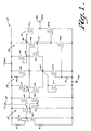
- the novel and improved MOS integrated circuit of this invention is shown to comprise an input buffer 10 having voltage level shifting means 12 incorporated MOS transistors M1-M6. All PMOS transistors are illustrated in Fig. 1 but it should be understood that other circuit components can also be incorporated in the improved input buffer 10 within the scope of this invention.
- the channels of the transistors M2 and M1 are connected in series between the source and drain supply voltages V ss and V dd .
- both transistors are depletion-type devices which are always on and the drain of transistor M2 is connected to the source of transistor M1 to form the node N1 as illustrated in Fig. 1.
- transistors M1 and M2 are connected to the drain supply voltage and to the source supply voltage respectively, preferably through respective current limiting resistors 14 and 16 which serve to protect the input buffer against static electricity.
- the transistor M1 is operated in the triode region to serve as a resistor and transistor M2 is always saturated to serve as a current source.
- the channels of transistors M4 and M3 are also connected in series between the source and drain supply voltages.
- the gate of transistor M3 is connected to node N1.
- the drain of transistor M4 is connected to the source of transistor M3 to form the node N2 as shown in Fig. 1 and that node N2 is connected to the gate of transistor M4.
- Both of the transistors M3 and M4 are enhancement-type devices and are proportioned and arranged so that they are always on to provide a relatively limited level of current.
- the channels of transistors M6 and M5 are also connected in series between the source and drain supply voltages, both of those transistors being enhancement-type devices.
- the gate of transistor M5 is connected to the input 18 of the buffer which is typically provided by an NMOS microprocessor or a transistor-transistor-logic (TTL) circuit or the like.
- the gate of the transistor M6 is connected to the node N2 in common with the gate of transistor M4 so that transistors M4 and M6 form a current mirror.
- the drain of transistor M6 is connected to the source of transistor M5 to form node N3 as is shown in Fig. 1.
- Transistors M3-M6 all operate in the saturation region.
- the level shifting means 12 cooperates with Schmitt trigger means 20 comprising the PMOS transistors M7-M12 and M17 which provides the input buffer 10 with desired hysteresis. That is, the channels of transistors M10 and M9 are connected in series between the source and drain supply voltages as shown in Fig. 1. The gates of the transistors M9 and M10 are connected to the drain and source supply voltages respectively, preferably through a respective current limiting resistors 22 and 24 for protecting the input buffer against static electricity.
- the transistor M9 is an enhancement-type device and transistors M10 and are depletion-type devices and the drain of M10 is connected to the source of M9 to form the node N5.
- Transistor M17 has its drain and gate connected to node N5 and its source connected to V ss .
- the channels of transistors M7 and M8 are connected in series between the drain supply voltage V dd and node N5 and the channels of transistors M11 and M12 are also connected in series between the drain supply voltage and node N5.
- Transistor M7 has its gate connected to its source and is also connected to the drain of transistor M8 to form node N4.
- the gate of transistor M8 is connected to node N3.
- Transistor M11 has its gate connected to its source and is also connected to the drain of transistor M12 to form node N6.
- the transistors M7, M10, M11 and M17 are depletion-type devices while transistors M8, M9 and M12 are enhancement devices. Transistors M7 and M11 are saturated while transistor M10 and M17 operate in the linear region.
- the input buffer 10 further includes the driver means 26 which preferably includes source follower, buffer means 28 comprising the transistors M13 and M14.
- the driver also includes an output stage 30 comprising the transistors M15 and M16.
- the channels of transistors M14 and M13 are connected in series between the source and drain supply voltages.
- the drain of depletion device M14 is connected to the source of enhancement device M13 to form the node N7 which is connected in common to the gate of transistor M12 in the Schmitt trigger 20.
- the gate of transistor M14 is connected to the source supply voltage, preferably through the static protection resistor 24 and the gate of transistor M13 is connected to node N4 in the Schmitt trigger.
- the two enhancement-type transistors M16 and M15 are connected in push-pull configuration between the source and drain supply voltages and the drain of transistor M16 is connected to the source of transistor M15 to form the output 34 of the buffer 10.
- the gate of transistor M16 is connected to the node N7 and the gate of transistor M15 is connected to the node N6 in the Schmitt trigger 20.
- the input buffer 10 is preferably arranged in an integrated circuit to receive logic signals from an NMOS microprocessor or the like.
- the source supply voltage V ss corresponds to the vehicle supply voltage and typically varies from 8 to 18 volts over an ambient temperature (t a ) range of -30°C. to 85°C. and is typically about 9.5v.
- the drain supply voltage V dd corresponds to system ground. In that arrangement, voltages at input 18 representing logic inputs "0" and "1" will be within a short range of V dd , typically in a range from V dd + 0.8v. to V dd + 3.5v. and neither input will approach V ss .
- the PMOS transistors M1-M17 have widths and lengths (W/L) in mils as set forth in Table I below: Table I Transistor W/L Transistor W/L M1 0.3/1.0 M9 0.3/2.4 M2 0.3/.60 M10 0.7/0.6 M3 0.3/1.0 M11 0.35/0.6 M4 18.0/0.60 M12 3.4/0.3 M5 0.3/1.0 M13 1.2/0.3 M6 18.0/0.60 M14 0.3/1.0 M7 0.3/1.0 M15 1.0/0.3 M8 1.4/0.3 M16 1.0/0.3 M17 0.7/0.6
- the input buffer 10 has the following input specifications: Min. Max. (1) V ss 8 volts 18 volts (2) t a -30°C. 85°C. (3) V IH 3.5 volts V ss plus .3 volts (4) V IL -0.3 volts 0.8 volts (5) Hysteresis 0.5 volts 0.8 volts (voltages stated with respect to V dd ) That is, where the source supply voltage varies from 8 to 18 volts, the input buffer is adapted to be responsive to logic high input voltages varying from 3.5 volts to V ss + 0.3 volts and to logic low input voltages varying from -0.3 volts to 0.8 volts while providing desired hysteresis of 0.5 volts.
- the buffer 10 provides level shifting, voltage and current gain, and desired hysteresis corresponding to the input specification as set forth above.
- the transistor M2 is always saturated and serves as a current source while the transistor M1 operates in the triode region and serves as a resistor, whereby a constant reference voltage V REF is generated at node N1, that voltage being referenced to V dd .
- the voltage V REF corresponds generally to the drain to source voltage across transistor M1 and varies with V dd such that as V dd varies between -8 and -18 volts, the reference voltage V REF varies between 3 volts and 4 volts.
- That voltage at N1 then serves to set the gate voltage at transistor M3 to provide the desired voltage level shifting. That is, the current I M3 in transistor M3 equals current I M4 in transistor M4; the current I M5 in transistor M5 equals current I M6 in transistor M6; the current I M4 equals the current I M6 ; and the voltage at node N2 corresponds to the threshold voltage V T of transistor M4.
- the voltage at node N3 therefore corresponds generally to the input voltage at 18 less the reference voltage V REF plus the noted threshold voltage V T .
- the transistors M3-M6 all operate in the saturation region since their gate voltages never exceed the drain supply voltage V dd .
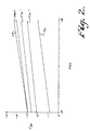
- the gate voltages provided at node N3 have logic levels of V T and V T + (V IH (min.) - V IL (max.)) which is ideal to drive the Schmitt trigger stage of the buffer as is illustrated in Fig. 2. That is, the low and high logic voltage levels L3 and H3 appearing at node N3 as voltages V IL (.8 volts) and V IH (3.5 volts) are applied at the input 18 respectively result in a minimum output of the level shifting means 12 as indicated by curves L3 and H3 in Fig. 2 as the drain supply voltage V dd varies between -8 and -18 volts.
- the Schmitt trigger means 20 are further adapted to cooperate with the level-shifting means 12 to assure proper operation of the buffer 10 over a wide range of operating conditions.
- the thresholds V TH + and V TH - of the Schmitt trigger are described by the following expressions: where I M7 , I M10 and I M11 are the currents in transistors M7, M10 and M11 respectively, R is a resistance across the parallel combination of transistors M10 and M17, and V TM8 is the threshold voltage of transistor M8.
- the transistors M7 and M11 are saturated and transistors M10 and M17 operate in the linear region.
- the hysteresis provided by the Schmitt trigger corresponds to I M11 R.
- transistors M7 and M8 form a first leg of the Schmitt trigger and transistors M11 and M12 form the second or alternate leg of the trigger which cooperate with transistors M10 and M17 to provide the trigger with selected hysteresis.
- the transistor M9 then acts as a resistor to the drain supply voltage and adds some dependence on drain supply voltage to both of the thresholds of the Schmitt trigger without affecting the hysteresis provided by the Schmitt trigger for noise suppression purposes.
- the Schmitt trigger compensates to some extent for the V dd dependence of the voltage at node N1 (due to the body effect of transistors M1 an M5) as previously described.
- the thresholds of the Schmitt trigger in the buffer 10 track the output of the level shifting means 12 over the range of variation of the drain supply voltage as is indicated at V TH + and V TH - in Fig. 2.
- the final output stage 26 of the buffer 10 then cooperates with the Schmitt trigger 20 in providing desired output voltage and drive current capabilities as will be understood. That is, the transistors M13 and M14 serve as a source follower to provide current gain and some additional shift of voltage level at node N7. The fairly large transistor M12 in the Schmitt trigger is then driven by the source follower as illustrated in Fig. 1 to improve the propogation delay achieved by the Schmitt trigger.
- the transistors M15 and M16 are arranged in push-pull configuration as shown and comprise a conventional buffer output stage.
- the buffer 10 typically receives a logic input from an NMOS microprocessor or the like so that the input voltage V IN at 18 varies within a short range of the drain supply voltage V dd and does not approach the level of the source supply voltage V ss .
- the buffer 10 is compatible with such an input from the microprocessor and serves as a noninverting input buffer to provide desired voltage and current levels for driving circuits including PMOS display driver means and the like in automotive applications.
- transistors M1 and M2 are always on and serve as a voltage divider to provide a reference voltage V REF at node N1. That reference voltage varies in the range from 3 volts to 4 volts as the drain supply voltage V dd varies from -8 to -18 volts and the voltage at N1 biases the level shifting components M3 - M6 to provide desirably level-shifted voltages at node N3. That is, the transistor M3 has the same size and resistance as transistor M5 and transistor M4 has the same size and resistance as transistor M6. Transistors M4 and M6 form a current mirror.
- Transistor M3 is biased by reference voltage V REF and serves as a voltage-to-current converter tending to provide a desired current level in transistor M4 and therefore in transistor M6.
- V REF reference voltage
- the voltage across transistor M5 corresponds to the voltage across transistor M3 and produces a desired level-shifting of the low and high voltages at node N3 away from V dd toward V ss as is indicated by curves L3 and H3 in Fig. 2.
- Those voltage levels at N3 then cooperate with the Schmitt trigger 20 and with the driver means 26 to provide an output 34 at desired voltage and current levels and with desired hysteresis for noise suppression purposes for driving the noted automotive control circuit.
- transistors M9 and M10 are always on in the Schmitt trigger 20 and the transistor M10 operates in the triode region to function as a resistor. There is accordingly a small current flowing in transistors M9 and M10 and M9 applies a selected voltage bias to node N5. Before transistor M8 is turned off as noted above, a small current also flows in transistor M7 and M8 providing additional voltage at the node N5 as will be understood. Then, when transistor M12 is turned on as noted above, transistor M11 has slightly less resistance than transistor M7 and provides a positive feedback so that the voltage at node N5 goes slightly toward V dd , thereby turning transistor M8 off more completely to provide the desired minimum .5 volt hysteresis as required by specification (5) noted above.
- nodes N4 and N6 are both outputs from the Schmitt trigger.
- the inverted output from node N4 is buffered through the source follower stage formed by transistors M13 and M14 and provides desired current gain while also cooperating with the noninverted output from node N6 in operating the final output stage of the buffer 10 as formed by the transistors M15 and M16.
- the input buffer 10 accomplishes the desired results and meets the desired input buffer specification utilizing a limited number of PMOS transistors of relatively limited size.
Landscapes
- Engineering & Computer Science (AREA)
- Computer Hardware Design (AREA)
- Physics & Mathematics (AREA)
- Computing Systems (AREA)
- General Engineering & Computer Science (AREA)
- Mathematical Physics (AREA)
- Logic Circuits (AREA)
- Manipulation Of Pulses (AREA)
Claims (5)
- Eingangspuffer einer integrierten MOS-Schaltung mit Mitteln (12) zur Pegelverschiebung, die abhängig von logischen Eingangssignalen mit ausgewählten Spannungspegeln entsprechende Steuersignale mit verschobenen Spannungspegeln liefern, mit Schmitt-Trigger-Mitteln (20) mit ausgewählten Schwellenspannungen, die abhängig davon, daß die Steuersignale die Schwellenspannungen überschreiten, entsprechende Trigger-Ausgangssignale mit Hysterese liefern, und mit Ausgangsmitteln (26), die abhängig von den Trigger-Ausgangssignalen Puffer-Ausgangssignale liefern, die eine verbesserte Kompatibilität für ein Ansteuern ausgewählter Schaltungsmittel aufweisen, wobei die Mittel zur Pegelverschiebung MOS-Transistormittel (M1, M2), die Spannungsteilermittel zum Liefern einer einen ausgewählten Pegel aufweisenden Referenzspannung bilden, zwei MOS-Transistormittel (M4, M6), die ein Stromspiegelmittel bilden, MOS-Transistormittel (M3), die durch die Referenzspanung vorgespannt sind, um erwünschte Strompegel in einem der Stromspiegel-Transistormittel liefern, und zusätzliche MOS-Transistormittel (M5) aufweisen, die so angeschlossen sind, daß sie die logischen Eingangssignale an ihrer Gate-Elektrode empfangen und auf die Stromspiegelmittel so ansprechen, daß gewährleistet wird, daß die entsprechenden Steuersignale mit den erwünschten, verschobenen Spannungspegeln geliefert werden.
- Puffer nach Anspruch 1, in welchem die Schmitt-Trigger-Mittel (20) erste Transistormittel (M10, M17), die zum Festlegen der ausgewählten Schwellenspannungen für die Schmitt-Trigger-Mittel ausgebildet sind, und zweite Transistormittel (M9) aufweisen, die zwischen die ersten Transistormittel und die eine Systemversorgungsspannung geschaltet sind und die Trigger-Schwellenspannungen von der Systemversorgungsspannung abhängig machen, so daß die Schwellenspannungen der Schmitt-Trigger-Mittel Änderungen in den entsprechenden Steuersignalen aufgrund von Veränderungen in der Versorgungsspannung folgen.
- Ein Puffer nach Anspruch 2, in welchem die auf die logischen Eingangssignale ansprechenden Mittel (12) erste PMOS-Schaltungsmittel (M5) aufweisen, die auf logische Eingangssignale ansprechen, deren Spannungspegel denjenigen entsprechen, die von einem PMOS-Schaltungsmittel zum Abgeben von entsprechenden, verschobene Spannungspegel aufweisenden Steuersignalen geliefert werden, wobei die Schmitt-Trigger-Mittel (20) zweite MOS-Schaltungsmittel (M7-M12, M17) aufweisen, die auf die pegelverschobenen Steuersignale ansprechen, um die entsprechenden Trigger-Ausgangssignale mit ausgewählter Hysterese zu liefern, und die Ausgangsmittel (26) PMOS-Schaltungsmittel (M13, M14, M15, M16) aufweisen, die abhängig von den Trigger-Ausgangssignalen zum Ansteuern eines externen integrierten PMOS-Schaltungsmittels geeignete Puffer-Ausgangssignale liefern.
- Puffer nach Anspruch 2 oder 3, in welchem die Schmitt-Trigger-Mittel zwei MOS-Transistormittel (M8, M12) aufweisen, die parallel angeordnet sind und mit ihren Source-Elektroden mit den ersten Transistormitteln (M10, M17), die eine gemeinsame Sourceimpedanz bilden, und mit den zweiten Transistormitteln (M9) verbunden sind, wobei die ersten und zweiten Transistormittel MOS-Transistoren enthalten.
- Puffer nach einem der vorhergehenden Ansprüche, in welchem die Ausgangsmittel Gegentaktverstärkermittel (M15, M16) und Source-Folgermittel (M13) enthalten, die auf die von den Schmitt-Trigger-Mitteln ausgegebenen Trigger-Ausgangssignale zum Ansteuern der Gegentaktverstärkermittel ansprechen, wobei die Source-Folgermittel (M13) auch zum Mitwirken beim Steuern der Schmitt-Trigger-Mittel ausgebildet sind, um die Schaltgeschwindigkeit des Puffers zu erhöhen.
Applications Claiming Priority (2)
| Application Number | Priority Date | Filing Date | Title |
|---|---|---|---|
| US514431 | 1983-07-18 | ||
| US06/514,431 US4553051A (en) | 1983-07-18 | 1983-07-18 | PMOS Input buffer compatible with logic inputs from an NMOS microprocessor |
Publications (3)
| Publication Number | Publication Date |
|---|---|
| EP0132148A2 EP0132148A2 (de) | 1985-01-23 |
| EP0132148A3 EP0132148A3 (en) | 1988-07-20 |
| EP0132148B1 true EP0132148B1 (de) | 1992-06-10 |
Family
ID=24047098
Family Applications (1)
| Application Number | Title | Priority Date | Filing Date |
|---|---|---|---|
| EP84304863A Expired EP0132148B1 (de) | 1983-07-18 | 1984-07-17 | PMOS-Eingangspuffer kompatibel mit logischen Eingängen von einem NMOS-Mikroprozessor |
Country Status (4)
| Country | Link |
|---|---|
| US (1) | US4553051A (de) |
| EP (1) | EP0132148B1 (de) |
| JP (1) | JP2594898B2 (de) |
| DE (1) | DE3485764T2 (de) |
Families Citing this family (5)
| Publication number | Priority date | Publication date | Assignee | Title |
|---|---|---|---|---|
| US4763021A (en) * | 1987-07-06 | 1988-08-09 | Unisys Corporation | CMOS input buffer receiver circuit with ultra stable switchpoint |
| US4956691A (en) * | 1989-03-24 | 1990-09-11 | Delco Electronics Corporation | NMOS driver circuit for CMOS circuitry |
| EP0417335A1 (de) * | 1989-09-11 | 1991-03-20 | Siemens Aktiengesellschaft | Schaltungsanordnung zur Wandlung von Signalen mit TTL-Pegel in Signale mit CML-Pegel oder ECL-Pegel |
| US7512019B2 (en) * | 2005-11-02 | 2009-03-31 | Micron Technology, Inc. | High speed digital signal input buffer and method using pulsed positive feedback |
| US8283946B2 (en) * | 2010-04-15 | 2012-10-09 | Micron Technology, Inc. | Signaling systems, preamplifiers, memory devices and methods |
Family Cites Families (10)
| Publication number | Priority date | Publication date | Assignee | Title |
|---|---|---|---|---|
| JPS5342587B2 (de) * | 1974-04-23 | 1978-11-13 | ||
| JPS5112222A (ja) * | 1974-07-19 | 1976-01-30 | Fujitsu Ltd | Toreinkaatoritsuji |
| JPS51139223A (en) * | 1975-05-28 | 1976-12-01 | Hitachi Ltd | Mis level converter circuit |
| US4023050A (en) * | 1976-05-10 | 1977-05-10 | Gte Laboratories Incorporated | Logic level converter |
| JPS54561A (en) * | 1977-06-03 | 1979-01-05 | Hitachi Ltd | Cathode ray tube of projection type |
| JPS5570993A (en) * | 1978-11-24 | 1980-05-28 | Hitachi Ltd | Memory circuit |
| US4342004A (en) * | 1979-05-15 | 1982-07-27 | Tokyo Shibaura Denki Kabushiki Kaisha | Voltage comparator circuit |
| DD143991A1 (de) * | 1979-05-24 | 1980-09-17 | Franz Roessler | Schaltungsanordnung fuer einen eingangsinverter in integrierter mis-technik |
| WO1982000930A1 (en) * | 1980-09-10 | 1982-03-18 | Plachno R | Delay stage for a clock generator |
| JPS5793731A (en) * | 1980-12-02 | 1982-06-10 | Nec Corp | Logical level conversion circuit |
-
1983
- 1983-07-18 US US06/514,431 patent/US4553051A/en not_active Expired - Fee Related
-
1984
- 1984-07-16 JP JP59146133A patent/JP2594898B2/ja not_active Expired - Fee Related
- 1984-07-17 DE DE8484304863T patent/DE3485764T2/de not_active Expired - Fee Related
- 1984-07-17 EP EP84304863A patent/EP0132148B1/de not_active Expired
Also Published As
| Publication number | Publication date |
|---|---|
| EP0132148A2 (de) | 1985-01-23 |
| US4553051A (en) | 1985-11-12 |
| JPS6039917A (ja) | 1985-03-02 |
| JP2594898B2 (ja) | 1997-03-26 |
| DE3485764T2 (de) | 1993-01-14 |
| DE3485764D1 (de) | 1992-07-16 |
| EP0132148A3 (en) | 1988-07-20 |
Similar Documents
| Publication | Publication Date | Title |
|---|---|---|
| US4438352A (en) | TTL Compatible CMOS input buffer | |
| US6229353B1 (en) | Source-coupled logic with reference controlled inputs | |
| US5381061A (en) | Overvoltage tolerant output buffer circuit | |
| US4471242A (en) | TTL to CMOS Input buffer | |
| EP0140677B1 (de) | Differentialverstärker mit einer Konstantstromquelle | |
| US5365127A (en) | Circuit for conversion from CMOS voltage levels to shifted ECL voltage levels with process compensation | |
| US6064229A (en) | Voltage translating buffer based on low voltage technology | |
| US5266887A (en) | Bidirectional voltage to current converter | |
| US6040729A (en) | Digital output buffer for multiple voltage system | |
| US11277121B1 (en) | Level shifter | |
| US4453121A (en) | Reference voltage generator | |
| JPH05145384A (ja) | Cmosレシーバ入力インターフエース回路 | |
| CA1047602A (en) | Voltage level conversion circuit | |
| US20020039042A1 (en) | Level shift circuit | |
| US4804868A (en) | BiMOS logical circuit | |
| EP1032132B1 (de) | Ausgangspuffer für differenzielle Niederspannugssignale | |
| US7230469B2 (en) | Multi-level/single ended input level shifter circuit | |
| EP0511856B1 (de) | Bezugsgenerator | |
| JP3492765B2 (ja) | レベル変換回路 | |
| WO1991005404A2 (en) | Current mirror | |
| EP0132148B1 (de) | PMOS-Eingangspuffer kompatibel mit logischen Eingängen von einem NMOS-Mikroprozessor | |
| US5047671A (en) | CMOS to ECL converter | |
| US5023479A (en) | Low power output gate | |
| EP0297722A2 (de) | ECL/NMOS-Pegelwandler | |
| EP0397335A2 (de) | CMOS-Pegelumsetzschaltung |
Legal Events
| Date | Code | Title | Description |
|---|---|---|---|
| PUAI | Public reference made under article 153(3) epc to a published international application that has entered the european phase |
Free format text: ORIGINAL CODE: 0009012 |
|
| AK | Designated contracting states |
Designated state(s): DE FR GB |
|
| PUAL | Search report despatched |
Free format text: ORIGINAL CODE: 0009013 |
|
| AK | Designated contracting states |
Kind code of ref document: A3 Designated state(s): DE FR GB |
|
| 17P | Request for examination filed |
Effective date: 19881122 |
|
| 17Q | First examination report despatched |
Effective date: 19890821 |
|
| GRAA | (expected) grant |
Free format text: ORIGINAL CODE: 0009210 |
|
| AK | Designated contracting states |
Kind code of ref document: B1 Designated state(s): DE FR GB |
|
| REF | Corresponds to: |
Ref document number: 3485764 Country of ref document: DE Date of ref document: 19920716 |
|
| ET | Fr: translation filed | ||
| PLBE | No opposition filed within time limit |
Free format text: ORIGINAL CODE: 0009261 |
|
| STAA | Information on the status of an ep patent application or granted ep patent |
Free format text: STATUS: NO OPPOSITION FILED WITHIN TIME LIMIT |
|
| 26N | No opposition filed | ||
| PGFP | Annual fee paid to national office [announced via postgrant information from national office to epo] |
Ref country code: GB Payment date: 20010614 Year of fee payment: 18 |
|
| PGFP | Annual fee paid to national office [announced via postgrant information from national office to epo] |
Ref country code: FR Payment date: 20010702 Year of fee payment: 18 |
|
| PGFP | Annual fee paid to national office [announced via postgrant information from national office to epo] |
Ref country code: DE Payment date: 20010731 Year of fee payment: 18 |
|
| REG | Reference to a national code |
Ref country code: GB Ref legal event code: IF02 |
|
| PG25 | Lapsed in a contracting state [announced via postgrant information from national office to epo] |
Ref country code: GB Free format text: LAPSE BECAUSE OF NON-PAYMENT OF DUE FEES Effective date: 20020717 |
|
| PG25 | Lapsed in a contracting state [announced via postgrant information from national office to epo] |
Ref country code: DE Free format text: LAPSE BECAUSE OF NON-PAYMENT OF DUE FEES Effective date: 20030201 |
|
| GBPC | Gb: european patent ceased through non-payment of renewal fee |
Effective date: 20020717 |
|
| PG25 | Lapsed in a contracting state [announced via postgrant information from national office to epo] |
Ref country code: FR Free format text: LAPSE BECAUSE OF NON-PAYMENT OF DUE FEES Effective date: 20030331 |
|
| REG | Reference to a national code |
Ref country code: FR Ref legal event code: ST |