EP0130910B1 - A sense amplifier - Google Patents
A sense amplifier Download PDFInfo
- Publication number
- EP0130910B1 EP0130910B1 EP84401375A EP84401375A EP0130910B1 EP 0130910 B1 EP0130910 B1 EP 0130910B1 EP 84401375 A EP84401375 A EP 84401375A EP 84401375 A EP84401375 A EP 84401375A EP 0130910 B1 EP0130910 B1 EP 0130910B1
- Authority
- EP
- European Patent Office
- Prior art keywords
- flip
- channel mos
- channel
- source
- sense amplifier
- Prior art date
- Legal status (The legal status is an assumption and is not a legal conclusion. Google has not performed a legal analysis and makes no representation as to the accuracy of the status listed.)
- Expired
Links
- 230000015654 memory Effects 0.000 claims description 16
- 230000004044 response Effects 0.000 claims description 3
- 239000004065 semiconductor Substances 0.000 claims description 3
- 229910044991 metal oxide Inorganic materials 0.000 claims 1
- 150000004706 metal oxides Chemical class 0.000 claims 1
- 230000007704 transition Effects 0.000 claims 1
- 230000008859 change Effects 0.000 description 10
- 238000010586 diagram Methods 0.000 description 8
- 230000008901 benefit Effects 0.000 description 4
- 230000001052 transient effect Effects 0.000 description 4
- 230000006870 function Effects 0.000 description 2
- 238000004519 manufacturing process Methods 0.000 description 2
- 230000004048 modification Effects 0.000 description 2
- 238000012986 modification Methods 0.000 description 2
- 230000003071 parasitic effect Effects 0.000 description 2
- 230000035945 sensitivity Effects 0.000 description 2
- 230000001133 acceleration Effects 0.000 description 1
- 238000010276 construction Methods 0.000 description 1
- 230000007423 decrease Effects 0.000 description 1
- 238000007599 discharging Methods 0.000 description 1
- 230000000694 effects Effects 0.000 description 1
- 230000000977 initiatory effect Effects 0.000 description 1
- 230000010354 integration Effects 0.000 description 1
- 238000002955 isolation Methods 0.000 description 1
- 238000000034 method Methods 0.000 description 1
- 230000005855 radiation Effects 0.000 description 1
Images

Classifications
-
- G—PHYSICS
- G11—INFORMATION STORAGE
- G11C—STATIC STORES
- G11C11/00—Digital stores characterised by the use of particular electric or magnetic storage elements; Storage elements therefor
- G11C11/56—Digital stores characterised by the use of particular electric or magnetic storage elements; Storage elements therefor using storage elements with more than two stable states represented by steps, e.g. of voltage, current, phase, frequency
- G11C11/5692—Digital stores characterised by the use of particular electric or magnetic storage elements; Storage elements therefor using storage elements with more than two stable states represented by steps, e.g. of voltage, current, phase, frequency read-only digital stores using storage elements with more than two stable states
-
- G—PHYSICS
- G11—INFORMATION STORAGE
- G11C—STATIC STORES
- G11C7/00—Arrangements for writing information into, or reading information out from, a digital store
- G11C7/06—Sense amplifiers; Associated circuits, e.g. timing or triggering circuits
- G11C7/065—Differential amplifiers of latching type
-
- G—PHYSICS
- G11—INFORMATION STORAGE
- G11C—STATIC STORES
- G11C7/00—Arrangements for writing information into, or reading information out from, a digital store
- G11C7/06—Sense amplifiers; Associated circuits, e.g. timing or triggering circuits
Definitions
- This invention relates to a sense amplifier for a semiconductor memory device, in particular, to that suited to a multi-level memory in which each memory cell stores a data represented by binary bits more than one.
- Fig. 1 is a partial circuit diagram of a four-level ROM device, showing a memory cell M e and sensing facilities including a load circuit LOAD, a column select transistor Q e , and three sense amplifiers, SA,, SA 2 and SA 3 , whose inputs are commonly connected to the data bus.
- the Q D1 designates a transistor for discharging the bit line prior to the selection of column and row.
- Sense amplifiers typically employed for memory devices are classified into two kinds; the one is a type of differential amplifier, and the other is that comprising a flip-flop circuit.
- a sense amplifier of the former type for sensing a multiple bit ROM has been disclosed in the U.S. Patent 4,287,570 filed September 1, 1981, for instance. From the point of view of sensitivity, a sense amplifier of the flip-flop type should be more advantageous than a sense amplifier of the differential amplifier type.
- U.S. Patent 4,163,233 discloses a radiation hardened CMOS sense amplifier featuring two cross-coupled inverter amplifier stages having components that can automatically compensate for the effect of electrical parameter nonuniformities.
- each input signal is two level, and the sense amplifier is only required to discriminate read-out signals whose levels change within a narrow range 1 volt just below the power source voltage.
- the sense amplifier is only required to discriminate read-out signals whose levels change within a narrow range 1 volt just below the power source voltage.
- three sense amplifiers must respond to four-level input signals varying in a range of a few volts, and it is necessary to provide means for isolating each fljp- flop type sense amplifier to let it function independently from the others.
- the solutions for these problems formerly resulted in the increase of operational delay in the flip-flop type sense amplifiers, particularly in those for ROMs.
- a couple of buffer circuits the first comprising n-channel MOS transistors Q 7 and Q e , and the second comprising n-channel MOS transistors Qg and Q, o , are respectively connected. That is, the conduction channels in each pair of transistors Q 7 and Q a and transistors Qg and Q, o are linked in series between a positive potential source (V cc ) and a negative potential source (V ss ), and the junction in each transistor pair is connected to each of the nodes P 1 and P 2 , respectively. Therefore, the buffer circuits are formed in a source follower mode.
- the gate of the transistor Q 7 receives a read-out signal D, while the gate of the transistor Qg receives a reference voltage Ref.
- the transistors Q 8 and Q 10 are designed to have a relatively lower conductance (gm) compared to that of the transistors Q 7 and Q 9 , hence the potentials at the nodes P 1 and P 2 change to be approximately equal to the level of D and Ref, respectively, during the stand-by sequence (the period in which the flip-flop circuit is not activated to output a full logic level signal).
- each of the switching circuits has CMOS inverter configuration.
- the conduction channel of a CMOS inverter constituting each switching circuit is connected between a positive potential source (V cc ) and a negative potential source (V 55 ), and the common gate of the CMOS inverter constituting the first switching circuit receives a first clock signal, CLK n , and the common gate of the CMOS inverter constituting the second switching circuit receives a second clock signal, CLK p .
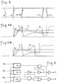
- the wave forms of the clock signals are shown in Fig. 3.
- each sense amplifier SA,, SA 2 and SA 3 For sensing the read-out signal from a four-level memory cell, three sense amplifiers SA,, SA 2 and SA 3 each having the circuit configuration as shown in Fig. 2 are implemented. Reference voltage signals Ref 1 , Ref 2 and Ref3 differing from one another in level are respectively input to each of the sense amplifiers. Thanks to the buffer circuit, each of the three sense amplifiers SA 1 , SA 2 and SA 3 whose input terminals are connected commonly to the data bus is isolated and can operate independently from the others.
- the potential at the node P 1 of the sense amplifier SA is pulled down to the level of the negative potential source V ss (usually the ground level) during latching operation.
- V ss usually the ground level
- the level at the node P, of each of the sense amplifiers SA 2 and SA 3 can be correctly pulled up to the level of the positive potential source V cc independently from the pull-down in the sense amplifier SA,.
- any multi-level read-out signal having a level in the range between the highest reference voltage Ref, and the lowest reference voltage Ref3 can be discriminated. It is obvious that such buffer circuit is unnecessary in the sense amplifier for an ordinary two-level memory device.
- CMOS configuration can provide a circuit of low power dissipation, however, further advantage of the CMOS is utilized in this invention. That is, a flip-flop circuit comprising CMOS inverters can operate to provide a full logic level output signal even either when both of the potentials at the nodes P 1 and P 2 are higher than the threshold voltage V th(p) of the p-channel MOS transistors Q 3 and Q 4 or when both of the potentials at the nodes P, and P 2 are lower than the threshold voltage V th(n) of the n-channel MOS transistors Q, and Q 2 .
- CMOS flip-flop circuit eliminates need for designing the flip-flop circuit for each sense amplifier individually to match the reference voltage input to the sense amplifier. That is, it is possible to produce sense amplifiers SA,, SA 2 and SA 3 which have identical circuit parameters, hence reducing cost and turn around time in the manufacturing.
- CMOS switching circuits connected to each common source of the flip-flop circuit is explained in connection with the wave form of the read-out signal D and the potential change at the nodes P, and P 2 .
- a control signal ⁇ o (which is for resetting the bit line to the ground level) turns to low level, hence the memory cell M e is ready for operation, then the gate of LOAD is open by the input of a control signal ⁇ 1 .
- a read-out signal D having level corresponding to the conductance (gm) of the selected memory cell is generated on the bit line.
- the reference voltage Ref of each predetermined level is generated in each of the three reference voltage signal generating circuits (not shown).
- the read-out signal D on the bit line is input commonly through the data bus to the sense amplifiers SA 1 , SA 2 and SA 3 , while three reference voltages Ref 1 , Ref 2 and Ref3 are respectively input to the sense amplifiers SA 1 , SA 2 and SA 3 .
- Figs. 4(A) and 4(B) are schematic diagrams showing the wave forms of the read-out voltage signal D, the reference voltage Ref, and the potentials at the nodes P, and P 2 of the flip-flop circuit shown in Fig. 2.
- Fig. 1 and Fig. 4(A) when the gate of the LOAD connected to the data bus is opened by incoming of the control signal ⁇ 1 , steep rise of potential on the data bus occurs as shown by the curve D in Fig. 4(A).
- the column select transistor Q c turns to ON by incoming of the column select signal COL, the potential falls very sharply, then tends to increase slowly to reach a steady level determined by the gm of the selected memory cell.
- This potential change in the curve D is due to the difference in the parasitic capacity of the data bus and that of the bit line. That is, the parasitic capacity of the data bus is substantially small compared to that of the bit line, accordingly, the time constant of the potential change on the data bus is small so long as the column select transistor Q c is OFF, but it becomes large after the column select transistor Q c has turned ON.
- the potential on the data bus rises steeply up to the level approximately equal to the positive potential source V cc .
- the potential fall occurring just after the turn on of the column select transistor Q c appears because the bit line has been reset to be in the ground level by the incoming of the control signal ⁇ o , as described above.
- the transient peak appears in the read-out voltage signal D.
- the potential change in the Ref is rather rapid and monotonous as shown by the curve Ref in Fig. 4(A).
- Potential change at the nodes P 1 and P 2 occurs as shown by the dashed line curves in the Fig. 4(A), in response to the changes of the read-out voltage signal D and the reference voltage Ref.
- the potential at the node P 1 rises sharply as in the rise of the potential D on the data bus, and reaches a level approximately equal to that of the D, (in the strict sense, P 1 is lower than D by V th , the threshold voltage of the transistor Q 7 of the first buffer circuit: see Fig. 2), but it decreases rather slowly to reach a steady level instead.
- the potential at the node P 2 changes approximately in parallel to the curve of the reference voltage Ref and reaches a steady level (the level at the node P 2 is lower than Ref by V th , the threshold voltage of the transistor Qg of the second buffer circuit: see Fig. 2).
- the large time constant in the fall of the level at the node P is due to the small conductance (gm) of the bias transistor Q B comprising the first buffer circuit.
- each of the curves representing the changes of the potentials at the nodes P, and P 2 cross each other, if the level of the read-out voltage signal D is lower than the level of the reference voltage Ref.
- the timing of the crossing depends on the heights of P 1 and P 2 at their steady levels. For example, in the four-level memory device, the largest delay of the timing occurs in the sense amplifier SA 3 when the lowest level read-out signal is input. Therefore, the timing to initiate the latching operation of the flip-flop circuits cannot be earlier than the above largest delay.
- the first clock signal CLK n turns to high level, hence, in the first switching circuit, transistor Q 5 is turned to OFF state while transistor Q 6 is turned to ON state.
- the second clock signal CLKp turns to low level, hence, in the second switching circuit, transistor Q 12 is turned to OFF state while transistor Q 11 is turned to ON state.
- the common source of the n-channel transistors Q, and Q 2 and that of the p-channel transistors Q 3 and Q 4 are respectively connected to negative potential source V ss and positive potential source V cc , and the flip-flop circuit is latched to amplify the potential difference between the node P, and P 2 up to the full logic level.
- timing when the second clock signal CLKp turns to low level may be same that when the first clock signal CLK n turns to high level, as far as it does not precede the latter.
- the full logic level signals output simultaneously from the three sense amplifiers are input to a decoder as shown in Fig. 5 and processed to provide a data represented by two binary bits. For instance, when assuming that each sense amplifier outputs a signal "1" if the level of the read-out signal D is higher than the level of its reference voltage Ref, and "0" if the level of the D is lower than that of the Ref, there may be four combinations of the output signals from the three sense amplifiers, i.e. 111, 110,100 and 000. They are related to the four states each represented by two bits of binary code, respectively, i.e. 11, 10, 01 and 00.
- the relation among the levels of the read-out signal D and the reference voltage Ref, the above combination of the output signal and the state represented by two binary bits is summarized in the following.
- the flip-flop circuit in the present invention is not only kept inactive by the isolation of the common source of the p-channel transistors from the positive potential source during the stand-by sequence, but it is, meanwhile, rather powered to accelerate the change of the potential at the input/output nodes by implementing a means for supplying each common source of the p-channel transistors and the n-channel transistors with respective inverted potential.
- the operational speed can be maintained high even in the sense amplifier responsive to discriminate a read-out voltage signal of the lowest level in a multi-level ROM.
- sufficient potential difference is provided between the nodes P, and P 2 in a relatively short period during stand-by sequence, therefore, sensitivity of a flip-flop type sense amplifier can be improved without sacrifice of the operational speed.
Landscapes
- Engineering & Computer Science (AREA)
- Computer Hardware Design (AREA)
- Static Random-Access Memory (AREA)
- Read Only Memory (AREA)
- Dram (AREA)
Description
- This invention relates to a sense amplifier for a semiconductor memory device, in particular, to that suited to a multi-level memory in which each memory cell stores a data represented by binary bits more than one.
- There has been proposed a concept of multi-level memory which is expected as a breakthrough forthe capacity limitation problem of semiconductor memory devices. (Electronics, October 39, 1980, p.39, ibid. June 30, 1982, p.81, etc.) This technique is for increasing the capacity of a memory device with a constant chip size without increasing integration density. Some of four-level type memory devices have been put into practical application as ROMs (Read Only Memories). In such ROMs, the level of read out signal from each memory cell is related to one of the four states (data) represented by two bits of binary. These data are usually written in as the difference of the conductivity of the MOS transistor constituting a memory cell, during manufacturing process of the memory device by altering the size of the gate area of each transistor. Therefore, such ROM fall into the category of mask ROM.
- In case of a four-level memory device, the level of each read-out signal is compared with three reference voltages, accordingly, it is necessary to implement at least three sense amplifiers each of which receives one of the three different reference voltages. Fig. 1 is a partial circuit diagram of a four-level ROM device, showing a memory cell Me and sensing facilities including a load circuit LOAD, a column select transistor Qe, and three sense amplifiers, SA,, SA2 and SA3, whose inputs are commonly connected to the data bus. In Fig. 1, the QD1 designates a transistor for discharging the bit line prior to the selection of column and row. As seen in Fig. 1, when the gate of LOAD is opened and the column select signal COL and row select signal ROW are respectively applied to the gates of the transistor Qe and the memory cell Me, a read-out signal of a specified level corresponding to the data stored in the memory cell Me is generated on the data bus and is applied to the sense amplifiers SA" SA2 and SA3, simultaneously.
- Sense amplifiers typically employed for memory devices are classified into two kinds; the one is a type of differential amplifier, and the other is that comprising a flip-flop circuit. A sense amplifier of the former type for sensing a multiple bit ROM has been disclosed in the U.S. Patent 4,287,570 filed September 1, 1981, for instance. From the point of view of sensitivity, a sense amplifier of the flip-flop type should be more advantageous than a sense amplifier of the differential amplifier type. U.S. Patent 4,163,233, for example, discloses a radiation hardened CMOS sense amplifier featuring two cross-coupled inverter amplifier stages having components that can automatically compensate for the effect of electrical parameter nonuniformities. However, it seems that there has been so far no disclosure of a flip-flop type sense amplifier which would be adapted to be used in multi-level memory devices. Though there are a lot of disclosures of flip-flop type sense amplifiers for the use in RAMs (Random Access Memories), such sense amplifier cannot be employed in the multi-level memory devices. This is due to the following problems.
- In a RAM, each input signal is two level, and the sense amplifier is only required to discriminate read-out signals whose levels change within a
narrow range 1 volt just below the power source voltage. On the other hand, in the four-level memory device, forexample, three sense amplifiers must respond to four-level input signals varying in a range of a few volts, and it is necessary to provide means for isolating each fljp- flop type sense amplifier to let it function independently from the others. Furthermore, the solutions for these problems formerly resulted in the increase of operational delay in the flip-flop type sense amplifiers, particularly in those for ROMs. - Therefore, it is the primary object of the present invention to provide a flip-flop type sense amplifier which is adaptable to a multi-level memory device, and is particularly suited to a multi-level ROM device.
- The sense amplifier of the present invention is defined in
Claim 1. - The objects, features and advantages of the present invention will appear more fully from the following description.
-
- Fig. 1 is a circuit diagram showing a part of a four-level ROM;
- Fig. 2 is a circuit diagram embodying a sense amplifier of the present invention;
- Fig. 3 is a schematic diagram showing the input timing of controlling pulses; and
- Figs. 4(A) and 4(B) are schematic diagrams showing potential changes in a sense amplifier.
- Fig. 5 is a circuit diagram of a decoder for converting output signals from three sense amplifiers into a two binary bits expression;
- Fig. 2 is a circuit diagram embodying a sense amplifier of the present invention. In Fig. 2, Q, and Q2 denote n-channel MOS transistors, and Q3 and Q4 (both attached with an arrowhead each) denote p-channel MOS transistors. Therefore each pair of Q, and Q3, and Q2 and Q4 constitutes a CMOS inverter. These CMOS inverters are cross-coupled each other of their input terminals (common gate) and output terminals (nodes), hence form a flip-flop circuit. To the nodes P, and P2 of the CMOS inverters, a couple of buffer circuits, the first comprising n-channel MOS transistors Q7 and Qe, and the second comprising n-channel MOS transistors Qg and Q,o, are respectively connected. That is, the conduction channels in each pair of transistors Q7 and Qa and transistors Qg and Q,o are linked in series between a positive potential source (Vcc) and a negative potential source (Vss), and the junction in each transistor pair is connected to each of the nodes P1 and P2, respectively. Therefore, the buffer circuits are formed in a source follower mode. The gate of the transistor Q7 receives a read-out signal D, while the gate of the transistor Qg receives a reference voltage Ref. The transistors Q8 and Q10 are designed to have a relatively lower conductance (gm) compared to that of the transistors Q7 and Q9, hence the potentials at the nodes P1 and P2 change to be approximately equal to the level of D and Ref, respectively, during the stand-by sequence (the period in which the flip-flop circuit is not activated to output a full logic level signal).
- To the common source of the n-channel transistors Q1 and Q2, and that of the p-channel transistors Q3 and Q4, a couple of switching circuits, the first comprising a p-channel MOS transistor Q5 and an n-channel MOS transistor Q6, the second comprising a p-channel transistor Q11 and n-channel transistor Q12, are respectively connected. Therefore, each of the switching circuits has CMOS inverter configuration. The conduction channel of a CMOS inverter constituting each switching circuit is connected between a positive potential source (Vcc) and a negative potential source (V55), and the common gate of the CMOS inverter constituting the first switching circuit receives a first clock signal, CLKn, and the common gate of the CMOS inverter constituting the second switching circuit receives a second clock signal, CLKp. The wave forms of the clock signals are shown in Fig. 3.
- For sensing the read-out signal from a four-level memory cell, three sense amplifiers SA,, SA2 and SA3 each having the circuit configuration as shown in Fig. 2 are implemented. Reference voltage signals Ref1, Ref2 and Ref3 differing from one another in level are respectively input to each of the sense amplifiers. Thanks to the buffer circuit, each of the three sense amplifiers SA1, SA2 and SA3 whose input terminals are connected commonly to the data bus is isolated and can operate independently from the others. For instance, when the level of the read-out signal D and the levels of the reference signals Ref1, Ref2 and Ref3 are in the following relation, the potential at the node P1 of the sense amplifier SA, is pulled down to the level of the negative potential source Vss (usually the ground level) during latching operation.

- Thus, any multi-level read-out signal having a level in the range between the highest reference voltage Ref, and the lowest reference voltage Ref3 can be discriminated. It is obvious that such buffer circuit is unnecessary in the sense amplifier for an ordinary two-level memory device.
- It is well known that CMOS configuration can provide a circuit of low power dissipation, however, further advantage of the CMOS is utilized in this invention. That is, a flip-flop circuit comprising CMOS inverters can operate to provide a full logic level output signal even either when both of the potentials at the nodes P1 and P2 are higher than the threshold voltage Vth(p) of the p-channel MOS transistors Q3 and Q4 or when both of the potentials at the nodes P, and P2 are lower than the threshold voltage Vth(n) of the n-channel MOS transistors Q, and Q2. In Fig. 2, if the potential V(P1) at the node P, and the potential V(P2) at the node P2 are in the following relation, for example,


- The function of the CMOS switching circuits connected to each common source of the flip-flop circuit is explained in connection with the wave form of the read-out signal D and the potential change at the nodes P, and P2. Referring to Figs. 1 and 3, in the stand-by sequence, a control signal φo (which is for resetting the bit line to the ground level) turns to low level, hence the memory cell Me is ready for operation, then the gate of LOAD is open by the input of a control signal φ1. Subsequently to the above, when the column select signal COL and the row select signal ROW which are respectively input to the gates of the column select transistor Qc and the memory cell Me turn to high level, a read-out signal D having level corresponding to the conductance (gm) of the selected memory cell is generated on the bit line. At the same time, the reference voltage Ref of each predetermined level is generated in each of the three reference voltage signal generating circuits (not shown). The read-out signal D on the bit line is input commonly through the data bus to the sense amplifiers SA1, SA2 and SA3, while three reference voltages Ref1, Ref2 and Ref3 are respectively input to the sense amplifiers SA1, SA2 and SA3.
- Figs. 4(A) and 4(B) are schematic diagrams showing the wave forms of the read-out voltage signal D, the reference voltage Ref, and the potentials at the nodes P, and P2 of the flip-flop circuit shown in Fig. 2. Referring to Fig. 1 and Fig. 4(A), when the gate of the LOAD connected to the data bus is opened by incoming of the control signal φ1, steep rise of potential on the data bus occurs as shown by the curve D in Fig. 4(A). On the other hand, when the column select transistor Qc turns to ON by incoming of the column select signal COL, the potential falls very sharply, then tends to increase slowly to reach a steady level determined by the gm of the selected memory cell. This potential change in the curve D is due to the difference in the parasitic capacity of the data bus and that of the bit line. That is, the parasitic capacity of the data bus is substantially small compared to that of the bit line, accordingly, the time constant of the potential change on the data bus is small so long as the column select transistor Qc is OFF, but it becomes large after the column select transistor Qc has turned ON. Thus, the potential on the data bus rises steeply up to the level approximately equal to the positive potential source Vcc. The potential fall occurring just after the turn on of the column select transistor Qc appears because the bit line has been reset to be in the ground level by the incoming of the control signal φo, as described above. Thus, the transient peak appears in the read-out voltage signal D. On the other hand, the potential change in the Ref is rather rapid and monotonous as shown by the curve Ref in Fig. 4(A).
- Potential change at the nodes P1 and P2 occurs as shown by the dashed line curves in the Fig. 4(A), in response to the changes of the read-out voltage signal D and the reference voltage Ref. The potential at the node P1 rises sharply as in the rise of the potential D on the data bus, and reaches a level approximately equal to that of the D, (in the strict sense, P1 is lower than D by Vth, the threshold voltage of the transistor Q7 of the first buffer circuit: see Fig. 2), but it decreases rather slowly to reach a steady level instead. The potential at the node P2 changes approximately in parallel to the curve of the reference voltage Ref and reaches a steady level (the level at the node P2 is lower than Ref by Vth, the threshold voltage of the transistor Qg of the second buffer circuit: see Fig. 2). The large time constant in the fall of the level at the node P, is due to the small conductance (gm) of the bias transistor QB comprising the first buffer circuit.
- In the course of reaching steady level, each of the curves representing the changes of the potentials at the nodes P, and P2 cross each other, if the level of the read-out voltage signal D is lower than the level of the reference voltage Ref. The timing of the crossing depends on the heights of P1 and P2 at their steady levels. For example, in the four-level memory device, the largest delay of the timing occurs in the sense amplifier SA3 when the lowest level read-out signal is input. Therefore, the timing to initiate the latching operation of the flip-flop circuits cannot be earlier than the above largest delay.
- However, in the sense amplifier of the present invention, earlier latching operation can be accomplished as follows. Referring to Fig. 2 and Fig. 3, the second clock signal CLKp is in high level during the stand-by sequence, hence the transistor Q,2 in the CMOS inverter constituting the second switching circuit is in ON state, and the common source of the p-channel transistors Q3 and Q4 of the flip-flop circuit is connected to the negative potential source Vss. Under this condition, charges accumulated in the capacity attached to the node P,, in response to the transient rise in the potential D, are discharged through the transistors Q3 and Q12 as far as the potential at the node P, is kept higherthan the potential at the node P2 by Vth(p), the threshold voltage of the p-channel transistor Q3. Consequently, the height of the transient peak in the potential change at the node P, is reduced, and further, the fall subsequent to the transient peak is accelerated, as shown in Fig. 4(B).
- At the same time, the transistor Q5 in the CMOS inverter constituting the first switching circuit is in ON state because the first clock signal CLKn is in low level, hence the common source of the n-channel transistors Q1 and Q2 of the flip-flop circuit is connected to the positive potential source Vcc. Under this condition, the charge-up of the capacity attached to the node P2 is accelerated through the transistor Q2 which is in ON state as far as the potential at the node P1 is kept higher than the potential at the node P2 by Vth(n), the threshold voltage of the n-channel transistor Q2. (Note that, in this sequence, transistor Q, is in OFF state).
- As the result of both accelerations in the discharge of the capacity attached to the node P, and in the charge-up of the capacity attached to the node P2, the crossing timing of the potentials at the nodes P1 and P2 is advanced, as shown in Fig. 4(B), and earlier initiation of the latching operation of the flip-flop circuit can be accomplished.
- After the crossing, the first clock signal CLKn turns to high level, hence, in the first switching circuit, transistor Q5 is turned to OFF state while transistor Q6 is turned to ON state. Subsequent to the change of the first clock signal CLKn, the second clock signal CLKp turns to low level, hence, in the second switching circuit, transistor Q12 is turned to OFF state while transistor Q11 is turned to ON state. Thus, the common source of the n-channel transistors Q, and Q2 and that of the p-channel transistors Q3 and Q4 are respectively connected to negative potential source Vss and positive potential source Vcc, and the flip-flop circuit is latched to amplify the potential difference between the node P, and P2 up to the full logic level. In the above operation, timing when the second clock signal CLKp turns to low level may be same that when the first clock signal CLKn turns to high level, as far as it does not precede the latter.
- The full logic level signals output simultaneously from the three sense amplifiers are input to a decoder as shown in Fig. 5 and processed to provide a data represented by two binary bits. For instance, when assuming that each sense amplifier outputs a signal "1" if the level of the read-out signal D is higher than the level of its reference voltage Ref, and "0" if the level of the D is lower than that of the Ref, there may be four combinations of the output signals from the three sense amplifiers, i.e. 111, 110,100 and 000. They are related to the four states each represented by two bits of binary code, respectively, i.e. 11, 10, 01 and 00. The relation among the levels of the read-out signal D and the reference voltage Ref, the above combination of the output signal and the state represented by two binary bits is summarized in the following.

- As described in the above embodiment, the flip-flop circuit in the present invention is not only kept inactive by the isolation of the common source of the p-channel transistors from the positive potential source during the stand-by sequence, but it is, meanwhile, rather powered to accelerate the change of the potential at the input/output nodes by implementing a means for supplying each common source of the p-channel transistors and the n-channel transistors with respective inverted potential. Hence, the operational speed can be maintained high even in the sense amplifier responsive to discriminate a read-out voltage signal of the lowest level in a multi-level ROM. In other words, sufficient potential difference is provided between the nodes P, and P2 in a relatively short period during stand-by sequence, therefore, sensitivity of a flip-flop type sense amplifier can be improved without sacrifice of the operational speed.
- The many features and advantages of the present invention are apparent from the detailed specification, and thus, it is intended by the appended claims to cover all such features and advantages of the device which fall within the true scope of the invention. Further, since modifications and changes will readily occur to those skilled in the art, it is not desired to limit the invention to the exact construction and operation illustrated and described, and accordingly, all suitable modifications and equivalents may be restored to, falling within the scope of the invention. For example, the above embodiment discloses the application to a multi-level ROM, however, the sense amplifier of the present invention can also be used in an ordinary two-level ROM or RAM.
Claims (3)
wherein the potentials at the common sources of said n-channel MOS transistors (Q,, Q2) and at the common source of said p-channel MOS transistors (Q3, Q4) are of mutually opposite polarities and are inverted in response to the transition between stand-by sequence and latching operation.
Applications Claiming Priority (2)
| Application Number | Priority Date | Filing Date | Title |
|---|---|---|---|
| JP58118618A JPS6010495A (en) | 1983-06-30 | 1983-06-30 | Sense amplifier |
| JP118618/83 | 1983-06-30 |
Publications (3)
| Publication Number | Publication Date |
|---|---|
| EP0130910A2 EP0130910A2 (en) | 1985-01-09 |
| EP0130910A3 EP0130910A3 (en) | 1987-10-28 |
| EP0130910B1 true EP0130910B1 (en) | 1990-09-05 |
Family
ID=14740999
Family Applications (1)
| Application Number | Title | Priority Date | Filing Date |
|---|---|---|---|
| EP84401375A Expired EP0130910B1 (en) | 1983-06-30 | 1984-06-28 | A sense amplifier |
Country Status (4)
| Country | Link |
|---|---|
| US (1) | US4558241A (en) |
| EP (1) | EP0130910B1 (en) |
| JP (1) | JPS6010495A (en) |
| DE (1) | DE3483121D1 (en) |
Families Citing this family (24)
| Publication number | Priority date | Publication date | Assignee | Title |
|---|---|---|---|---|
| JPS6177198A (en) * | 1984-09-21 | 1986-04-19 | Toshiba Corp | Semiconductor memory |
| JPS62102499A (en) * | 1985-10-28 | 1987-05-12 | Nec Corp | Memory circuit |
| US4663546A (en) * | 1986-02-20 | 1987-05-05 | Motorola, Inc. | Two state synchronizer |
| NL8602295A (en) * | 1986-09-11 | 1988-04-05 | Philips Nv | SEMI-CONDUCTOR MEMORY CIRCUIT WITH FAST READING AMPLIFIER TRISTATEBUS DRIVER. |
| US4769564A (en) * | 1987-05-15 | 1988-09-06 | Analog Devices, Inc. | Sense amplifier |
| KR920001325B1 (en) * | 1989-06-10 | 1992-02-10 | 삼성전자 주식회사 | Sense amp driver of memory device |
| KR920013458A (en) * | 1990-12-12 | 1992-07-29 | 김광호 | Differential Detection Amplifier |
| US6002614A (en) | 1991-02-08 | 1999-12-14 | Btg International Inc. | Memory apparatus including programmable non-volatile multi-bit memory cell, and apparatus and method for demarcating memory states of the cell |
| US5218569A (en) | 1991-02-08 | 1993-06-08 | Banks Gerald J | Electrically alterable non-volatile memory with n-bits per memory cell |
| JPH0750556A (en) * | 1993-08-09 | 1995-02-21 | Fujitsu Ltd | Flip-flop type amplifier circuit |
| EP0658000A3 (en) * | 1993-12-08 | 1996-04-03 | At & T Corp | A fast comparator circuit. |
| KR0140161B1 (en) * | 1994-12-29 | 1998-07-15 | 김주용 | Detector circuit of memory cell |
| US6353554B1 (en) | 1995-02-27 | 2002-03-05 | Btg International Inc. | Memory apparatus including programmable non-volatile multi-bit memory cell, and apparatus and method for demarcating memory states of the cell |
| KR0164385B1 (en) * | 1995-05-20 | 1999-02-18 | 김광호 | Sense amplifier circuit |
| JP3625930B2 (en) * | 1995-10-26 | 2005-03-02 | 株式会社日立製作所 | Semiconductor integrated circuit device |
| US6857099B1 (en) * | 1996-09-18 | 2005-02-15 | Nippon Steel Corporation | Multilevel semiconductor memory, write/read method thereto/therefrom and storage medium storing write/read program |
| US6031403A (en) * | 1996-11-13 | 2000-02-29 | International Business Machines Corporation | Pull-up and pull-down circuits |
| US5828239A (en) * | 1997-04-14 | 1998-10-27 | International Business Machines Corporation | Sense amplifier circuit with minimized clock skew effect |
| US6002626A (en) * | 1997-08-01 | 1999-12-14 | International Business Machines Corporation | Method and apparatus for memory cell array boost amplifier |
| US5892725A (en) * | 1998-05-13 | 1999-04-06 | International Business Machines Corporation | Memory in a data processing system having uneven cell grouping on bitlines and method therefor |
| US6819144B2 (en) * | 2003-03-06 | 2004-11-16 | Texas Instruments Incorporated | Latched sense amplifier with full range differential input voltage |
| US7847576B2 (en) * | 2009-02-26 | 2010-12-07 | Advantest Corporation | Comparator with latching function |
| US20110187414A1 (en) * | 2010-02-01 | 2011-08-04 | Taiwan Semiconductor Manufacturing Company, Ltd. | Pbti tolerant circuit design |
| US11095273B1 (en) * | 2020-07-27 | 2021-08-17 | Qualcomm Incorporated | High-speed sense amplifier with a dynamically cross-coupled regeneration stage |
Family Cites Families (13)
| Publication number | Priority date | Publication date | Assignee | Title |
|---|---|---|---|---|
| US3879621A (en) * | 1973-04-18 | 1975-04-22 | Ibm | Sense amplifier |
| US4007381A (en) * | 1975-04-18 | 1977-02-08 | Bell Telephone Laboratories, Incorporated | Balanced regenerative charge detection circuit for semiconductor charge transfer devices |
| US4031522A (en) * | 1975-07-10 | 1977-06-21 | Burroughs Corporation | Ultra high sensitivity sense amplifier for memories employing single transistor cells |
| US4169233A (en) * | 1978-02-24 | 1979-09-25 | Rockwell International Corporation | High performance CMOS sense amplifier |
| US4223394A (en) * | 1979-02-13 | 1980-09-16 | Intel Corporation | Sensing amplifier for floating gate memory devices |
| US4287570A (en) * | 1979-06-01 | 1981-09-01 | Intel Corporation | Multiple bit read-only memory cell and its sense amplifier |
| JPS56290A (en) * | 1979-06-11 | 1981-01-06 | Sumitomo Alum Smelt Co Ltd | Electrolytic furnace for production of aluminum |
| JPS5939840B2 (en) * | 1980-05-12 | 1984-09-26 | セイコーエプソン株式会社 | Read-only memory |
| US4376987A (en) * | 1980-08-18 | 1983-03-15 | Mcdonnell Douglas Corporation | Threshold referenced MNOS sense amplifier |
| US4461965A (en) * | 1980-08-18 | 1984-07-24 | National Semiconductor Corporation | High speed CMOS sense amplifier |
| DE3101520A1 (en) * | 1981-01-19 | 1982-08-26 | Siemens AG, 1000 Berlin und 8000 München | MONOLITHICALLY INTEGRATED SEMICONDUCTOR MEMORY |
| US4412143A (en) * | 1981-03-26 | 1983-10-25 | Ncr Corporation | MOS Sense amplifier |
| US4485317A (en) * | 1981-10-02 | 1984-11-27 | Fairchild Camera & Instrument Corp. | Dynamic TTL input comparator for CMOS devices |
-
1983
- 1983-06-30 JP JP58118618A patent/JPS6010495A/en active Pending
-
1984
- 1984-06-28 EP EP84401375A patent/EP0130910B1/en not_active Expired
- 1984-06-28 DE DE8484401375T patent/DE3483121D1/en not_active Expired - Fee Related
- 1984-07-02 US US06/626,795 patent/US4558241A/en not_active Expired - Lifetime
Also Published As
| Publication number | Publication date |
|---|---|
| US4558241A (en) | 1985-12-10 |
| EP0130910A3 (en) | 1987-10-28 |
| DE3483121D1 (en) | 1990-10-11 |
| JPS6010495A (en) | 1985-01-19 |
| EP0130910A2 (en) | 1985-01-09 |
Similar Documents
| Publication | Publication Date | Title |
|---|---|---|
| EP0130910B1 (en) | A sense amplifier | |
| US4899066A (en) | OR-type CMOS logic circuit with fast precharging | |
| US4751681A (en) | Dynamic differential amplifier | |
| US4616143A (en) | High voltage bootstrapping buffer circuit | |
| EP0328110B1 (en) | Operation mode setting circuit for DRAM | |
| US3983412A (en) | Differential sense amplifier | |
| US6205079B1 (en) | Semiconductor integrated circuit having power-supply circuits for producing internal supply voltages | |
| US4754170A (en) | Buffer circuit for minimizing noise in an integrated circuit | |
| US4514829A (en) | Word line decoder and driver circuits for high density semiconductor memory | |
| US5574687A (en) | Semiconductor memory | |
| US4104733A (en) | Address selecting circuitry for semiconductor memory device | |
| US4733112A (en) | Sense amplifier for a semiconductor memory device | |
| US4825110A (en) | Differential amplifier circuit | |
| EP0220870A2 (en) | An interface circuit for converting ECL signal levels to fet logic signal levels | |
| US5157284A (en) | Integrated circuit including an input buffer circuit having nand and nor gates | |
| US4704706A (en) | Booster circuit | |
| US4943945A (en) | Reference voltage generator for precharging bit lines of a transistor memory | |
| US5729159A (en) | Multiple reference sense amplifier | |
| US4843595A (en) | Data reading circuit for semiconductor memory device | |
| EP0168246B1 (en) | Improved active pull-up circuit | |
| US4831590A (en) | Semiconductor memory including an output latch having hysteresis characteristics | |
| US4893029A (en) | Power supply noise protection circuit | |
| KR950005171B1 (en) | Current mirror amplifier and driving method | |
| US6002624A (en) | Semiconductor memory device with input/output masking function without destruction of data bit | |
| US4554469A (en) | Static bootstrap semiconductor drive circuit |
Legal Events
| Date | Code | Title | Description |
|---|---|---|---|
| PUAI | Public reference made under article 153(3) epc to a published international application that has entered the european phase |
Free format text: ORIGINAL CODE: 0009012 |
|
| AK | Designated contracting states |
Designated state(s): DE FR GB |
|
| PUAL | Search report despatched |
Free format text: ORIGINAL CODE: 0009013 |
|
| AK | Designated contracting states |
Kind code of ref document: A3 Designated state(s): DE FR GB |
|
| 17P | Request for examination filed |
Effective date: 19880120 |
|
| 17Q | First examination report despatched |
Effective date: 19890404 |
|
| GRAA | (expected) grant |
Free format text: ORIGINAL CODE: 0009210 |
|
| AK | Designated contracting states |
Kind code of ref document: B1 Designated state(s): DE FR GB |
|
| REF | Corresponds to: |
Ref document number: 3483121 Country of ref document: DE Date of ref document: 19901011 |
|
| ET | Fr: translation filed | ||
| PLBE | No opposition filed within time limit |
Free format text: ORIGINAL CODE: 0009261 |
|
| STAA | Information on the status of an ep patent application or granted ep patent |
Free format text: STATUS: NO OPPOSITION FILED WITHIN TIME LIMIT |
|
| 26N | No opposition filed | ||
| PGFP | Annual fee paid to national office [announced via postgrant information from national office to epo] |
Ref country code: GB Payment date: 19930408 Year of fee payment: 10 |
|
| PGFP | Annual fee paid to national office [announced via postgrant information from national office to epo] |
Ref country code: FR Payment date: 19930629 Year of fee payment: 10 |
|
| PGFP | Annual fee paid to national office [announced via postgrant information from national office to epo] |
Ref country code: DE Payment date: 19930830 Year of fee payment: 10 |
|
| PG25 | Lapsed in a contracting state [announced via postgrant information from national office to epo] |
Ref country code: GB Effective date: 19940628 |
|
| GBPC | Gb: european patent ceased through non-payment of renewal fee |
Effective date: 19940628 |
|
| PG25 | Lapsed in a contracting state [announced via postgrant information from national office to epo] |
Ref country code: FR Effective date: 19950228 |
|
| PG25 | Lapsed in a contracting state [announced via postgrant information from national office to epo] |
Ref country code: DE Effective date: 19950301 |
|
| REG | Reference to a national code |
Ref country code: FR Ref legal event code: ST |