EP0129982A2 - Rückwandverdrahtung - Google Patents
Rückwandverdrahtung Download PDFInfo
- Publication number
- EP0129982A2 EP0129982A2 EP84303463A EP84303463A EP0129982A2 EP 0129982 A2 EP0129982 A2 EP 0129982A2 EP 84303463 A EP84303463 A EP 84303463A EP 84303463 A EP84303463 A EP 84303463A EP 0129982 A2 EP0129982 A2 EP 0129982A2
- Authority
- EP
- European Patent Office
- Prior art keywords
- power supply
- backpanel
- printed circuit
- pins
- pcb
- Prior art date
- Legal status (The legal status is an assumption and is not a legal conclusion. Google has not performed a legal analysis and makes no representation as to the accuracy of the status listed.)
- Granted
Links
Images

Classifications
-
- H—ELECTRICITY
- H05—ELECTRIC TECHNIQUES NOT OTHERWISE PROVIDED FOR
- H05K—PRINTED CIRCUITS; CASINGS OR CONSTRUCTIONAL DETAILS OF ELECTRIC APPARATUS; MANUFACTURE OF ASSEMBLAGES OF ELECTRICAL COMPONENTS
- H05K7/00—Constructional details common to different types of electric apparatus
- H05K7/14—Mounting supporting structure in casing or on frame or rack
- H05K7/1438—Back panels or connecting means therefor; Terminals; Coding means to avoid wrong insertion
- H05K7/1457—Power distribution arrangements
-
- H—ELECTRICITY
- H05—ELECTRIC TECHNIQUES NOT OTHERWISE PROVIDED FOR
- H05K—PRINTED CIRCUITS; CASINGS OR CONSTRUCTIONAL DETAILS OF ELECTRIC APPARATUS; MANUFACTURE OF ASSEMBLAGES OF ELECTRICAL COMPONENTS
- H05K1/00—Printed circuits
- H05K1/02—Details
- H05K1/14—Structural association of two or more printed circuits
Definitions
- This invention relates to backpanel assemblies. It is well known to provide electronic equipment, such as telecommunications equipment, with a backpanel having a plurality of elongate printed circuit board (PC8) connectors aligned in parallel thereon, into which PCBs are inserted to carry out desired functions.
- the backpanel which for example is itself a multi-layer printed circuit board, provides desired interconnections between the PCBs, and enables the supply of signals and power thereto, via the PCB connectors.
- an object of this invention is to provide a backpanel assembly which facilitates the supply of power to PCBs inserted into PCB connectors of the backpanel selectively from single or multiple power supplies.
- a backpanel assembly comprising a main backpanel having a plurality of elongate printed circuit board (PCB) connectors aligned in parallel thereon, the backpanel having a part extending beyond an end of the PCB connectors, the assembly including a plurality of power supply studs and a plurality of power supply pins, in respect of each of the PCB connectors, on said extending part of the backpanel, and printed circuit wiring interconnecting each power supply stud with at least one power supply pin and with the associated PCB connector, whereby power can be supplied to printed circuit boards, inserted into the PCB connectors, selectively via the associated power supply studs or via the associated power supply pins.
- PCB printed circuit board
- the power supply studs alone, or the power supply pins alone, or the studs and pins in combination can be used to supply power to printed circuit boards when these are inserted into the PCB connectors.
- these are arranged in lines across the extending part of the backpanel, whereby corresponding studs associated with the different PCB connectors can be interconnected by a power supply bus for supplying power commonly to printed circuit boards inserted into the PCB connectors.
- the power supply studs and the power supply pins preferably extend from the extending part of the backpanel on opposite sides thereof, so that such power supply buses do not impede access to the pins, and vice versa.
- the printed circuit wiring interconnects a plurality of power supply pins to a power supply stud.
- a backpanel assembly in accordance with the invention can initially comprise the main backpanel and be supplied with power via the power supply buses and studs from a single power source, and can subsequently be extended by removal of the power supply buses and provision of an additional, power supply backpanel as described below with associated power supply PCBs, for individually powering the printed circuit boards inserted into the PCB connectors of the main backpanel.
- an additional, power supply backpanel as described below with associated power supply PCBs, for individually powering the printed circuit boards inserted into the PCB connectors of the main backpanel.
- the invention also extends to electronic equipment including a backpanel assembly as recited above.
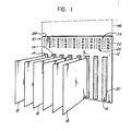
- a backpanel assembly 10 comprising a main backpanel 12 having a plurality of elongate printed circuit board (PCB) connectors 14 aligned in parallel thereon.
- PCB printed circuit board
- the connectors 14 can be of any known form, conveniently each connector 14 consists_of two rows of pins 18 surrounded by a shroud 20 which serves to protect the pins and to guide connector on a printed circuit board 16 into engagement and electrical contact with the pins when the PCB 16 is inserted into the connector 14. Arrangements of such pins and shrouds are known and are not further described here.
- each set of power supply pins 24 consists of two rows of pins which extend adjacent to an upper edge 28 of the b ackpanel 12. The power supply pins 24 are conveniently aligned with the pins 18 of the respective connectors 14.
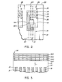
- Fig. 2 illustrates in greater detail an arrangement of the pins 24 and studs 26 in relation to one of the connectors 14.
- the shroud 20 of the connector in Fig. 2 is represented by a broken line in order to distinguish it clearly from printed circuit wiring described below.
- the backpanel 12 comprises a 4-layer printed circuit board having two signal circuit planes, one on each face of the board, and a power supply circuit plane and a ground plane sandwiched therebetween. It is also assumed that the power supply circuit plane has printed circuit wiring for three power supply lines, for example for voltages of +5V, +12V, and -12V relative to ground. Accordingly, in Fig.
- each set of power supply studs 26 consists of four studs 30, 32, 34, and 36 which are respectively connected to the ground plane (not shown, for the sake of clarity), a +12V power supply printed circuit track 38, a -12V power supply printed circuit track 40, and a +5V power supply printed circuit track 42, which is wider than the tracks 38 and 40 to enable it to carry a greater current.
- the tracks 38, 40, and 42 provide electrical connections between the power supply studs 32, 34, and 36, respective pins of the associated connector 14, and respective power supply pins 24.
- Fig. 2 illustrates each of the tracks 38 and 40 connecting to two of the pins 24 and two of the pins 18, and illustrates the track 42 connecting to four of the pins 24 and four of the pins 18.
- These tracks are individually provided in respect of the different connectors 14, so that printed circuit boards inserted into the respective connectors 14 are supplied with power separately from their respective sets of power supply pins 18 or 24.
- each stud 30 is connected via the ground plane to another one or more of the pins 18 and to other pins 24 of the respective connector 14.
- the ground plane may extend commonly between the various connectors 14 and the respective power supply studs and pins.
- the uppermost six power supply pins 24, i.e. those nearest to the upper edge 28 of the backpanel 12, may be connected to the ground plane.
- Other pins 24, which are not connected as illustrated in Fig. 2 may also be connected to the ground plane 24 to provide additional ground connections, or may be connected to one of the signal planes to provide signal path connections, or may be omitted.
- Figs. 1 and 2 it is assumed that the pins 24 extend from the backpanel 12 towards the viewer, whereas the studs 26 extend from the opposite face of the backpanel 12 away from the viewer, so that only the back ends of the studs are shown in Figs. 1 and 2.
- Fig. 3 illustrates part of the reverse side of the backpanel 12, showing that printed circuit boards 16 may also be inserted in connectors 14 additionally provided on this reverse side of the backpanel 12.
- the pins 18 conveniently extend completely through the backpanel 12 to form parts of the connectors 14 on both sides of the backpanel in known manner.
- each power supply bus consists of a conductive metal bar having holes therein through which the respective studs extend, the studs being threaded and provided with nuts (not shown) to clamp the bar to the studs.
- each individual power supply on a PCB 44 consists of d.c. to d.c. converters for producing the desired power supply voltages from the 48 volt power supply of a telephone central office.
- Fig. 4 includes an additional, power supply, backpanel 46 (the position of which is also illustrated in broken lines in Fig. 1) which is the same width as the backpanel 12 and which is mounted to extend upwardly therefrom in the same plane as the backpanel 12.
- the backpanel 46 has a lower edge 48 which abuts the upper edge 28 of the backpanel 12 so that the two backpanels are contiguous.
- shrouds 52 are mounted on the backpanel 46 to extend beyond its lower edge 48, each shroud 52 surrounding a respective set of pins 50, and also surrounding the corresponding set of pins 24 on the backpanel 12 when the two backpanels are contiguously arranged as in Fig. 4, to form therewith a respective PCB connector for a power supply PCB 44.
- the connectors formed by the shrouds 52 are similar to the connectors 14, except that they bridge the edges 28, 48 of the backpanels and surround and align pins on both backpanels.
- the shrouds 52 can optionally also be secured to the backpanel 12.
- a power supply PCB 44 is inserted into the corresponding connector formed by a shroud 52, pins 50, and pins 24, to supply the board 16 individually.
- Printed circuit wiring (not shown) on the backpanel 46 serves to supply power from the common, reliable, power source to respective ones of each set of pins 50, from whence power is delivered to the individual boards 16 via the d.c. to d.c. converters on the respective power supply PCB 44, the respective set of pins 24, and the respective printed circuit wiring of the backpanel 12 described above with reference to Fig. 2.
- Fig. 5 illustrates an arrangement for supplying power individually via the backpanel 46 and two power supply PCBs 44, to two groups 54, 56 of connectors 14, and thence to PCBs 16 inserted into these connectors, the connectors 14 of each group being powered commonly by respective power supply buses interconnecting the power supply studs 26 associated with these connectors.
- Fig. 5 there are two sets of power supply buses, shown by broken lines because they are on the reverse side of the backpanel 12, which interconnect the left-hand four and the right hand four sets of power supply studs 26 respectively.
- the power supply buses and the power supply PCBs 44 and their connectors do not interfere physically with one another because they are on opposite sides of the backpanels.
Landscapes
- Engineering & Computer Science (AREA)
- Microelectronics & Electronic Packaging (AREA)
- Power Engineering (AREA)
- Coupling Device And Connection With Printed Circuit (AREA)
- Catalysts (AREA)
- Transition And Organic Metals Composition Catalysts For Addition Polymerization (AREA)
- Chemical Or Physical Treatment Of Fibers (AREA)
- Mounting Of Printed Circuit Boards And The Like (AREA)
- Structure Of Printed Boards (AREA)
- Connection Or Junction Boxes (AREA)
Priority Applications (1)
| Application Number | Priority Date | Filing Date | Title |
|---|---|---|---|
| AT84303463T ATE36438T1 (de) | 1983-06-23 | 1984-05-22 | Rueckwandverdrahtung. |
Applications Claiming Priority (2)
| Application Number | Priority Date | Filing Date | Title |
|---|---|---|---|
| CA000431114A CA1187204A (en) | 1983-06-23 | 1983-06-23 | Backpanel assemblies |
| CA431114 | 1983-06-23 |
Publications (3)
| Publication Number | Publication Date |
|---|---|
| EP0129982A2 true EP0129982A2 (de) | 1985-01-02 |
| EP0129982A3 EP0129982A3 (en) | 1986-02-26 |
| EP0129982B1 EP0129982B1 (de) | 1988-08-10 |
Family
ID=4125541
Family Applications (1)
| Application Number | Title | Priority Date | Filing Date |
|---|---|---|---|
| EP84303463A Expired EP0129982B1 (de) | 1983-06-23 | 1984-05-22 | Rückwandverdrahtung |
Country Status (7)
| Country | Link |
|---|---|
| EP (1) | EP0129982B1 (de) |
| JP (1) | JPH0785516B2 (de) |
| AT (1) | ATE36438T1 (de) |
| CA (1) | CA1187204A (de) |
| DE (1) | DE3473396D1 (de) |
| IE (1) | IE55827B1 (de) |
| PT (1) | PT78783A (de) |
Cited By (4)
| Publication number | Priority date | Publication date | Assignee | Title |
|---|---|---|---|---|
| EP0207496A2 (de) * | 1985-07-01 | 1987-01-07 | Bull HN Information Systems Inc. | Rückwand mit integrierter Schaltung |
| EP0230637A1 (de) * | 1986-01-16 | 1987-08-05 | BBC Brown Boveri AG | Speisungs- oder Anpassungsschaltung |
| DE8902022U1 (de) * | 1989-02-21 | 1989-04-27 | I R S Industrie Rationalisierungs Systeme Gmbh, 6100 Darmstadt, De | |
| WO1998041074A1 (de) * | 1997-03-13 | 1998-09-17 | Siemens Aktiengesellschaft | Elektrische verbindungsmittel für baugruppenträger |
Families Citing this family (2)
| Publication number | Priority date | Publication date | Assignee | Title |
|---|---|---|---|---|
| DE9016053U1 (de) * | 1990-11-26 | 1991-02-14 | Forschungsinstitut Prof. Dr.-Ing.Habil, Dr.Phil.Nat. Karl Otto Lehmann, Nachf. Gmbh & Cie, 7570 Baden-Baden, De | |
| DE4341505A1 (de) * | 1993-12-06 | 1995-06-14 | Sel Alcatel Ag | Gestell der Nachrichtentechnik |
Citations (2)
| Publication number | Priority date | Publication date | Assignee | Title |
|---|---|---|---|---|
| US3368117A (en) * | 1966-06-13 | 1968-02-06 | Ncr Co | Voltage distribution circuit arrangements for high-density packaging of electronic systems |
| US3564343A (en) * | 1968-09-24 | 1971-02-16 | Reliance Electric Co | Computer programming apparatus |
Family Cites Families (1)
| Publication number | Priority date | Publication date | Assignee | Title |
|---|---|---|---|---|
| JPS5843830Y2 (ja) * | 1979-01-29 | 1983-10-04 | 富士通株式会社 | 電子・通信機器装置 |
-
1983
- 1983-06-23 CA CA000431114A patent/CA1187204A/en not_active Expired
-
1984
- 1984-05-22 AT AT84303463T patent/ATE36438T1/de not_active IP Right Cessation
- 1984-05-22 DE DE8484303463T patent/DE3473396D1/de not_active Expired
- 1984-05-22 EP EP84303463A patent/EP0129982B1/de not_active Expired
- 1984-06-22 JP JP59127642A patent/JPH0785516B2/ja not_active Expired - Lifetime
- 1984-06-22 PT PT78783A patent/PT78783A/pt not_active IP Right Cessation
- 1984-06-22 IE IE1579/84A patent/IE55827B1/en not_active IP Right Cessation
Patent Citations (2)
| Publication number | Priority date | Publication date | Assignee | Title |
|---|---|---|---|---|
| US3368117A (en) * | 1966-06-13 | 1968-02-06 | Ncr Co | Voltage distribution circuit arrangements for high-density packaging of electronic systems |
| US3564343A (en) * | 1968-09-24 | 1971-02-16 | Reliance Electric Co | Computer programming apparatus |
Cited By (6)
| Publication number | Priority date | Publication date | Assignee | Title |
|---|---|---|---|---|
| EP0207496A2 (de) * | 1985-07-01 | 1987-01-07 | Bull HN Information Systems Inc. | Rückwand mit integrierter Schaltung |
| EP0207496B1 (de) * | 1985-07-01 | 1992-04-22 | Bull HN Information Systems Inc. | Rückwand mit integrierter Schaltung |
| EP0230637A1 (de) * | 1986-01-16 | 1987-08-05 | BBC Brown Boveri AG | Speisungs- oder Anpassungsschaltung |
| US4789792A (en) * | 1986-01-16 | 1988-12-06 | Bbc Brown, Boveri Ltd. | Feeding of matching circuit |
| DE8902022U1 (de) * | 1989-02-21 | 1989-04-27 | I R S Industrie Rationalisierungs Systeme Gmbh, 6100 Darmstadt, De | |
| WO1998041074A1 (de) * | 1997-03-13 | 1998-09-17 | Siemens Aktiengesellschaft | Elektrische verbindungsmittel für baugruppenträger |
Also Published As
| Publication number | Publication date |
|---|---|
| JPS6020600A (ja) | 1985-02-01 |
| ATE36438T1 (de) | 1988-08-15 |
| EP0129982A3 (en) | 1986-02-26 |
| IE55827B1 (en) | 1991-01-30 |
| DE3473396D1 (en) | 1988-09-15 |
| CA1187204A (en) | 1985-05-14 |
| PT78783A (en) | 1984-07-01 |
| EP0129982B1 (de) | 1988-08-10 |
| JPH0785516B2 (ja) | 1995-09-13 |
| IE841579L (en) | 1984-12-23 |
Similar Documents
| Publication | Publication Date | Title |
|---|---|---|
| US4511950A (en) | Backpanel assemblies | |
| RU2013897C1 (ru) | Электронная система | |
| US4179172A (en) | Modular hardware packaging apparatus | |
| US4331370A (en) | Connection system for printed circuit boards | |
| US5411416A (en) | Docking connector unit | |
| US5293636A (en) | Module for insertion into a multi-module system having electronic keying for preventing power to improperly connected modules with improperly configured diode connections | |
| US5442170B1 (en) | Programmable cable adaptor for connecting different automobile computers to diagnostic equipment | |
| EP0886219A3 (de) | Rechnerserversystem mit drahtlosen und redundanten Adapterkarten auf einer Eingang/Ausgangkarte | |
| US3993936A (en) | Connector arrangement for printed circuit card | |
| KR870005562A (ko) | 배선판 | |
| US5875091A (en) | Busbars with filter capacitors | |
| US6356966B1 (en) | System and method for bridging bus segments on a backplane and coupling single board computers to a backplane | |
| US20020090844A1 (en) | Segmented replaceable backplane system for electronic apparatus | |
| EP0731992B1 (de) | Verbindungstechnik hoher dichte | |
| US4862326A (en) | Power supply contact | |
| US20020060906A1 (en) | Interconnecting method of wiring in printed circuit boards and printed circuit board unit | |
| EP0129982B1 (de) | Rückwandverdrahtung | |
| EP0692927A2 (de) | Verbesserte Leiterplatte und Verfahren | |
| US20070015409A1 (en) | Reconfigurable interconnection device for electrical bundles | |
| US5061190A (en) | Double density backward and forward compatible card edge connector system | |
| US3560799A (en) | Bus bar building block assembly | |
| US4226492A (en) | Electrical interconnection apparatus | |
| EP0302351B1 (de) | Elektronisches Gerät | |
| US20030057779A1 (en) | Electronic module interconnect system | |
| US6721821B1 (en) | Apparatus for electronic data storage |
Legal Events
| Date | Code | Title | Description |
|---|---|---|---|
| PUAI | Public reference made under article 153(3) epc to a published international application that has entered the european phase |
Free format text: ORIGINAL CODE: 0009012 |
|
| AK | Designated contracting states |
Designated state(s): AT CH DE FR GB LI NL SE |
|
| PUAL | Search report despatched |
Free format text: ORIGINAL CODE: 0009013 |
|
| AK | Designated contracting states |
Designated state(s): AT CH DE FR GB LI NL SE |
|
| 17P | Request for examination filed |
Effective date: 19860408 |
|
| 17Q | First examination report despatched |
Effective date: 19870811 |
|
| GRAA | (expected) grant |
Free format text: ORIGINAL CODE: 0009210 |
|
| AK | Designated contracting states |
Kind code of ref document: B1 Designated state(s): AT CH DE FR GB LI NL SE |
|
| REF | Corresponds to: |
Ref document number: 36438 Country of ref document: AT Date of ref document: 19880815 Kind code of ref document: T |
|
| REF | Corresponds to: |
Ref document number: 3473396 Country of ref document: DE Date of ref document: 19880915 |
|
| ET | Fr: translation filed | ||
| PLBE | No opposition filed within time limit |
Free format text: ORIGINAL CODE: 0009261 |
|
| STAA | Information on the status of an ep patent application or granted ep patent |
Free format text: STATUS: NO OPPOSITION FILED WITHIN TIME LIMIT |
|
| 26N | No opposition filed | ||
| PGFP | Annual fee paid to national office [announced via postgrant information from national office to epo] |
Ref country code: AT Payment date: 19920512 Year of fee payment: 9 |
|
| PGFP | Annual fee paid to national office [announced via postgrant information from national office to epo] |
Ref country code: SE Payment date: 19920521 Year of fee payment: 9 |
|
| PGFP | Annual fee paid to national office [announced via postgrant information from national office to epo] |
Ref country code: CH Payment date: 19920525 Year of fee payment: 9 |
|
| PGFP | Annual fee paid to national office [announced via postgrant information from national office to epo] |
Ref country code: NL Payment date: 19920531 Year of fee payment: 9 |
|
| PG25 | Lapsed in a contracting state [announced via postgrant information from national office to epo] |
Ref country code: AT Effective date: 19930522 |
|
| PG25 | Lapsed in a contracting state [announced via postgrant information from national office to epo] |
Ref country code: SE Effective date: 19930523 |
|
| PG25 | Lapsed in a contracting state [announced via postgrant information from national office to epo] |
Ref country code: LI Effective date: 19930531 Ref country code: CH Effective date: 19930531 |
|
| PG25 | Lapsed in a contracting state [announced via postgrant information from national office to epo] |
Ref country code: NL Effective date: 19931201 |
|
| NLV4 | Nl: lapsed or anulled due to non-payment of the annual fee | ||
| REG | Reference to a national code |
Ref country code: CH Ref legal event code: PL |
|
| EUG | Se: european patent has lapsed |
Ref document number: 84303463.8 Effective date: 19931210 |
|
| REG | Reference to a national code |
Ref country code: GB Ref legal event code: IF02 |
|
| PGFP | Annual fee paid to national office [announced via postgrant information from national office to epo] |
Ref country code: GB Payment date: 20030417 Year of fee payment: 20 |
|
| PGFP | Annual fee paid to national office [announced via postgrant information from national office to epo] |
Ref country code: FR Payment date: 20030422 Year of fee payment: 20 |
|
| PGFP | Annual fee paid to national office [announced via postgrant information from national office to epo] |
Ref country code: DE Payment date: 20030530 Year of fee payment: 20 |
|
| REG | Reference to a national code |
Ref country code: FR Ref legal event code: CD |
|
| PG25 | Lapsed in a contracting state [announced via postgrant information from national office to epo] |
Ref country code: GB Free format text: LAPSE BECAUSE OF EXPIRATION OF PROTECTION Effective date: 20040521 |
|
| REG | Reference to a national code |
Ref country code: GB Ref legal event code: PE20 |