EP0129132A1 - Measuring device to detect a temperature difference - Google Patents
Measuring device to detect a temperature difference Download PDFInfo
- Publication number
- EP0129132A1 EP0129132A1 EP84106350A EP84106350A EP0129132A1 EP 0129132 A1 EP0129132 A1 EP 0129132A1 EP 84106350 A EP84106350 A EP 84106350A EP 84106350 A EP84106350 A EP 84106350A EP 0129132 A1 EP0129132 A1 EP 0129132A1
- Authority
- EP
- European Patent Office
- Prior art keywords
- resistor
- switch
- temperature
- measuring
- operational amplifier
- Prior art date
- Legal status (The legal status is an assumption and is not a legal conclusion. Google has not performed a legal analysis and makes no representation as to the accuracy of the status listed.)
- Granted
Links
Images


Classifications
-
- G—PHYSICS
- G01—MEASURING; TESTING
- G01K—MEASURING TEMPERATURE; MEASURING QUANTITY OF HEAT; THERMALLY-SENSITIVE ELEMENTS NOT OTHERWISE PROVIDED FOR
- G01K1/00—Details of thermometers not specially adapted for particular types of thermometer
- G01K1/02—Means for indicating or recording specially adapted for thermometers
- G01K1/028—Means for indicating or recording specially adapted for thermometers arrangements for numerical indication
-
- G—PHYSICS
- G01—MEASURING; TESTING
- G01K—MEASURING TEMPERATURE; MEASURING QUANTITY OF HEAT; THERMALLY-SENSITIVE ELEMENTS NOT OTHERWISE PROVIDED FOR
- G01K3/00—Thermometers giving results other than momentary value of temperature
- G01K3/08—Thermometers giving results other than momentary value of temperature giving differences of values; giving differentiated values
- G01K3/10—Thermometers giving results other than momentary value of temperature giving differences of values; giving differentiated values in respect of time, e.g. reacting only to a quick change of temperature
Definitions
- the invention relates to a measuring device for detecting a temperature difference with two temperature measuring resistors, which are connected on the one hand to a constant current source via a first or second switch and on the other hand to a reference potential via a common reference resistor, the connection point of each temperature measuring resistor being connected to the first or second switch a third or fourth switch and a resistor are connected to a first input of an operational amplifier connected as an integrator, the second input of which is connected to the reference resistor, a fifth switch connecting the first input of the operational amplifier to the reference potential and the switches being controlled in this way that the voltages applied to the temperature measuring resistors are converted into digital values using the dual slope method.
- Such a measuring device is known from DE-OS 30 32 091.
- the difference between two temperatures detected with temperature measuring resistors is converted into a digital value using the known dual slope method. If the measuring device is operated with a battery, low power consumption, i.e. short measuring times, to be observed.
- a method is therefore proposed in which the difference is not formed from zero to the current measured value, but from the highest expected measured value to the current measured value, when the dual slope method is integrated upward.
- a voltage divider becomes a special one Reference point formed.
- a further differential amplifier is provided, by means of which two field effect transistors, each in series with the temperature measuring resistors, are driven. This known method for shortening the measurement period is therefore associated with a high outlay on components. The necessary voltage divider and the additional operational amplifiers also consume additional energy. Finally, the measurement error is increased, if only slightly.
- the object of the invention is therefore to design a measuring device of the type mentioned at the outset in such a way that a shortening of the measuring period is achieved with little expenditure on components and without a deterioration in the measuring accuracy.
- the measuring period is understood to mean the entire time period for converting the voltages present at the temperature measuring resistors into digital values.
- the first input of the operational amplifier is connected to the reference potential via a compensation resistor, the compensation resistor being dimensioned such that the integration current through the integration capacitor is zero at a measuring temperature below a desired temperature measuring range.
- the resistance value of the temperature measuring resistors does not drop below a certain basic value.
- This basic value is compensated with the compensation resistance, i.e. in this case the integration current is zero. Since the integration no longer applies to the entire resistance value of the temperature measuring resistors, but only the portion that exceeds the basic value, the measuring period is significantly shortened.
- An impedance converter connected in an ideal diode switch can advantageously be connected upstream of the resistor.
- the impedance converter prevents the measurement result from being falsified by internal resistances of the switches, the integrator being completely decoupled from the measuring circuit by the ideal diode circuit during the integration of the reference voltage.
- a further resistor can advantageously be connected in series to the compensation resistor, with a controllable switch connected in parallel, the controllable switch being closed during the constant integration times provided in the dual slope method.
- a comparison resistor can be provided, which is connected on the one hand via a switch (18) to the constant current source and on the other hand to the reference resistor, with a switch (19) connecting the switch (18) and comparison resistor with the connection point of the switches ( 6, 7) connects, the switches (18, 19) being controlled in such a way that the voltage drop across the comparison resistor is also converted into a digital value using the dual slope method, and the determination of the measurement temperatures detected by the temperature measurement resistors by forming the difference between them corresponding digital values with the digital value assigned to the comparison resistor. The determination of the absolute measuring temperatures, which are required in addition to the temperature difference in some applications, is thus traced back to a difference formation.
- the arrangement according to the invention would otherwise have the disadvantage that errors occur due to the compensation resistance in the determination of absolute measuring temperatures, which, however, disappear again when the difference is formed.
- two temperature measuring resistors 1 and 2 are provided, each of which is associated with measuring points whose temperature difference is to be recorded.
- the temperature measuring resistors 1 and 2 are connected on the one hand via a switch 4 or 5 to a constant current source 14 and on the other hand via a common reference resistor 3 to the reference potential of the circuit.
- the connection point between temperature measuring resistor 1 and switch 4 or temperature measuring resistor 2 and switch 5 is connected via a switch 6 or 7 to the non-inverting input of an operational amplifier 9a.
- the non-inverting input of the operational amplifier 9a is also connected to the reference potential via a further switch 8.
- the output of the operational amplifier 9a is fed back to its inverting input via a diode 9b.
- the diode 9b is connected via a resistor 10 to the inverting input of an operational amplifier 11a.
- the output of the operational amplifier 11a is fed back to its inverting input via a capacitor 11b.
- the operational amplifier 11a with the capacitor 11b therefore acts as an integrator.
- the inverting input of the operational amplifier 11a is connected to the reference potential via a compensation resistor 12 and the non-inverting input is connected to the connection point of temperature measuring resistors 1, 2 and reference resistor 3.
- the Integrator 11 is followed by a comparator 13, which controls an evaluation circuit 17.
- Switches 4 to 8 are controlled by a control circuit (not shown) for the sake of clarity so that with the arrangement an analog-to-digital conversion of the voltages present at the temperature measuring resistors 1, 2 according to, for example, Tietze-Schenk "semiconductor circuit technology" pages 536, 537 known double integration method, also called dual slope method, takes place.
- FIG. 2 shows the profile of the output voltage U 11 of the integrator 11 in the individual switching phases of a measuring period.
- the reference symbols of the respectively closed switches are plotted in connection with the respective switching phases.
- the phase zero only serves to bring the output voltage of the integrator 11 to a defined output value.
- the switches 4 and 8 are closed so that the integrator 11 is highly integrated until the threshold voltage U 13 of the comparator 13 is reached.
- the switch 8 is opened and the switch 6 is closed, the switch 4 remaining closed.
- the integrator 11 thus integrates the measuring voltage at the temperature measuring resistor 1 for a fixed period of time, the integration current J i being reduced by the resistor 12 via the capacitor 11b.
- the switch 6 is opened in phase 2 and the switch 8 is closed, while the switch 4 remains closed.
- a phase 3 the switches 5 and 7 are closed and the voltage applied to the temperature measuring resistor 2 is integrated for a constant period of time, the integration current J i being reduced again by the resistor 12.
- switch 7 is opened and switch 8 is closed, while switch 5 remains closed.
- the voltage drop across the reference resistor 3 is again integrated during a phase 4.
- the period of time until the output voltage U 11 of the integrator 11 reaches the comparison value U 13 is again recorded by counting the pulses emitted by a comparator during this period, so that a digital value is present which is linearly related to the second measurement temperature.
- R F drops out in the counter if the offset voltage does not change between the successive phases within a measurement period. Long-term changes and temperature drift have no influence.
- the internal resistances of switches 4 and 5 have no influence on the measuring accuracy, since the current is impressed. Internal resistance changes of the switches 6 and 7 could, however, lead to errors without an impedance converter 9, since they are included in the integration time constant. However, the impedance converter 9 connected upstream of the operational amplifier 11a is so high-impedance on the input side that large changes in resistance of the switches 6 and 7 can be permitted. The reverse currents of the switches 4 to 8 can be neglected, since one of the switches 6, 7 or 8 is always closed and the resistors 1 to 3 are very low.
- the measuring times ie the duration of phases 2 and 4 only change by approximately 25% when the temperature changes from, for example, 20 ° to 90 ° - corresponding to a change in resistance from, for example, 540 ohms to 770 ohms.
- the measuring time at the lower limit of the temperature measuring range be zero by compensating the resistance value of the temperature measuring resistors at the lower measuring range limit, for example at 0 ° C. with the resistor 12.
- the inverting input of the operational amplifier 11a is at reference potential via the resistor 12, while the impedance converter with the upstream circuit part is completely decoupled from the operational amplifier 11a by means of the diode 9b.
- the measuring time i.e. the duration of phases 2 and 4 can be shortened, but the measurement time change for a given temperature change and thus the resolution remains the same.
- the constant times of phases 1 and 3 are kept as short as possible. If these constant times were shortened without further measures, the measurement time differences and thus the resolution would also be reduced accordingly.
- a further measuring branch with a constant comparison resistor 17 is provided, which is connected on the one hand via a switch 18 to the constant current source 14 and on the other hand to the reference resistor 3.
- the connection point of switch 18 and comparison resistor 17 is connected via a switch 19 to the input of the impedance converter 9.
- the circuit corresponds to the exemplary embodiment according to FIG. 3.
- the voltage applied to the comparative resistor 17 is also converted into a digital value.
- the measuring temperature detected with each temperature measuring resistor 1 and 2 can thus be determined individually by forming the difference with the constant value obtained in this way. By forming the difference, the absolute temperatures of the measuring resistors 1 and 2 can be determined just as precisely as their differential temperature.
Abstract
Description
Die Erfindung betrifft eine Meßeinrichtung zur Erfassung einer Temperaturdifferenz mit zwei Temperaturmeßwiderständen, die einerseits über einen ersten bzw. zweiten Schalter mit einer Konstantstromquelle und andererseits über einen gemeinsamen Referenzwiderstand mit einem Bezugspotential verbunden sind, wobei jeweils der Verbindungspunkt jedes Temperaturmeßwiderstandes mit ersten bzw. zweitem Schalter über einen dritten bzw. vierten Schalter und einen Widerstand mit einem ersten Eingang eines als Integrator beschalteten Operationsverstärkers verbunden ist, dessen zweiter Eingang mit dem Referenzwiderstand verbunden ist, wobei ein fünfter Schalter den ersten Eingang des Operationsverstärkers mit dem Bezugspotential verbindet und wobei die Schalter so angesteuert werden, daß die an den Temperaturmeßwiderständen anstehenden Spannungen nach dem Dual-Slope-Verfahren in Digitalwerte umgesetzt werden.The invention relates to a measuring device for detecting a temperature difference with two temperature measuring resistors, which are connected on the one hand to a constant current source via a first or second switch and on the other hand to a reference potential via a common reference resistor, the connection point of each temperature measuring resistor being connected to the first or second switch a third or fourth switch and a resistor are connected to a first input of an operational amplifier connected as an integrator, the second input of which is connected to the reference resistor, a fifth switch connecting the first input of the operational amplifier to the reference potential and the switches being controlled in this way that the voltages applied to the temperature measuring resistors are converted into digital values using the dual slope method.
Eine derartige Meßeinrichtung ist aus der DE-OS 30 32 091 bekannt. Dabei wird die Differenz zweier mit Temperaturmeßwiderständen erfaßter Temperaturen mit Hilfe des bekannten Dual-Slope-Verfahrens in einen Digitalwert umgesetzt. Wenn man die Meßeinrichtung mit einer Batterie betreibt, so ist auf geringen Stromverbrauch, d.h. kurze Meßzeiten, zu achten.Such a measuring device is known from DE-OS 30 32 091. The difference between two temperatures detected with temperature measuring resistors is converted into a digital value using the known dual slope method. If the measuring device is operated with a battery, low power consumption, i.e. short measuring times, to be observed.
In der genannten Offenlegungsschrift wird daher ein Verfahren vorgeschlagen, bei dem bei der Aufwärtsintegration des Dual-Slope-Verfahrens die Differenz nicht von Null bis zum aktuellen Meßwert, sondern vom höchsten zu erwartenden Meßwert bis zum aktuellen Meßwert gebildet wird. Damit werden die Integrationszeiten und somit auch der Stromverbrauch der Schaltung wesentlich kleiner. Zur Realisierung dieses Gedankens wird mit einem Spannungsteiler ein besonderer Bezugspunkt gebildet. Ferner ist ein weiterer Differenzverstärker vorgesehen, über den zwei jeweils in Serie zu den Temperaturmeßwiderständen liegende Feldeffekttransistoren angesteuert werden. Dieses bekannte Verfahren zur Verkürzung der Meßperiode ist also mit einem hohen Bauteileaufwand verbunden. Der notwendige Spannungsteiler und die zusätzlichen Operationsverstärker verbrauchen außerdem wieder zusätzliche Energie. Schließlich wird der Meßfehler - wenn auch nur geringfügig - erhöht.In the aforementioned publication, a method is therefore proposed in which the difference is not formed from zero to the current measured value, but from the highest expected measured value to the current measured value, when the dual slope method is integrated upward. As a result, the integration times and thus the power consumption of the circuit are significantly reduced. To realize this idea, a voltage divider becomes a special one Reference point formed. Furthermore, a further differential amplifier is provided, by means of which two field effect transistors, each in series with the temperature measuring resistors, are driven. This known method for shortening the measurement period is therefore associated with a high outlay on components. The necessary voltage divider and the additional operational amplifiers also consume additional energy. Finally, the measurement error is increased, if only slightly.
Aufgabe der Erfindung ist es daher, eine Meßeinrichtung der eingangs genannten Art so auszugestalten, daß eine Verkürzung der Meßperiode mit geringem Bauteileaufwand und ohne Verschlechterung der Meßgenauigkeit erreicht wird. Unter Meßperiode wird dabei die gesamte Zeitdauer zur Umsetzung der an den Temperaturmeßwiderständen anstehenden Spannungen in Digitalwerte verstanden.The object of the invention is therefore to design a measuring device of the type mentioned at the outset in such a way that a shortening of the measuring period is achieved with little expenditure on components and without a deterioration in the measuring accuracy. The measuring period is understood to mean the entire time period for converting the voltages present at the temperature measuring resistors into digital values.
Diese Aufgabe wird erfindungsgemäß dadurch gelöst, daß der erste Eingang des Operationsverstärkers über einen Kompensationswiderstand mit dem Bezugspotential verbunden ist, wobei der Kompensationswiderstand so dimensioniert ist, daß bei einer unterhalb eines gewünschten Temperatur-Meßbereichs liegenden Meßtemperatur der Integrationsstrom durch den Integrationskondensator Null ist.This object is achieved in that the first input of the operational amplifier is connected to the reference potential via a compensation resistor, the compensation resistor being dimensioned such that the integration current through the integration capacitor is zero at a measuring temperature below a desired temperature measuring range.
Bei der erfindungsgemäßen Lösung wird also davon ausgegangen, daß der Widerstandswert der Temperaturmeßwiderstände nicht unter einen bestimmten Grundwert sinkt. Dieser Grundwert wird mit dem Kompensationswiderstand kompensiert, d.h. der Integrationsstrom beträgt in diesem Fall Null. Da bei der Integration damit nicht mehr der gesamte Widerstandswert der Temperaturmeßwiderstände zur Geltung kommt, sondern nur noch der den Grundwert übersteigende Anteil, wird die Meßperiode wesentlich verkürzt.In the solution according to the invention it is therefore assumed that the resistance value of the temperature measuring resistors does not drop below a certain basic value. This basic value is compensated with the compensation resistance, i.e. in this case the integration current is zero. Since the integration no longer applies to the entire resistance value of the temperature measuring resistors, but only the portion that exceeds the basic value, the measuring period is significantly shortened.
Vorteilhafterweise kann dem Widerstand ein in Idealdiodenschalter geschalteter Impedanzwandler vorgeschaltet sein. Durch den Impedanzwandler wird eine Verfälschung des Meßergebnisses durch Innenwiderstände der Schalter verhindert, wobei durch die Idealdiodenschaltung der Integrator während der Integration der Referenzspannung völlig vom Meßkreis entkoppelt ist. Dem Kompensationswiderstand kann vorteilhafterweise ein weiterer Widerstand in Reihe geschaltet sein, dem ein steuerbarer Schalter parallelgeschaltet ist, wobei der steuerbare Schalter während der beim Dual-Slope-Verfahren vorgesehenen konstanten Integrationszeiten geschlossen wird. Durch die Verkleinerung des für den Integrator wirksamen Widerstandes während der konstanten Integrationszeiten können diese verkürzt werden, ohne daß auch die Meßzeitdifferenzen bei vorgegebener Temperaturdifferenz kleiner werden. Letztere dürfen zur Erzielung einer ausreichenden Auflösung nämlich nicht zu klein werden. Damit wird nochmals eine Verkürzung der gesamten Meßperiode erreicht.An impedance converter connected in an ideal diode switch can advantageously be connected upstream of the resistor. The impedance converter prevents the measurement result from being falsified by internal resistances of the switches, the integrator being completely decoupled from the measuring circuit by the ideal diode circuit during the integration of the reference voltage. A further resistor can advantageously be connected in series to the compensation resistor, with a controllable switch connected in parallel, the controllable switch being closed during the constant integration times provided in the dual slope method. By reducing the resistance effective for the integrator during the constant integration times, these can be shortened without the measurement time differences also becoming smaller for a given temperature difference. The latter must not be too small to achieve sufficient resolution. This shortens the entire measuring period again.
In einer vorteilhaften Ausführung kann ein Vergleichswiderstand vorgesehen sein, der einerseits über einen Schalter (18) an die Konstantstromquelle und andererseits an den Referenzwiderstand angeschlossen ist, wobei ein Schalter (19) den Verbindungspunkt von Schalter (18) und Vergleichswiderstand mit dem Verbindungspunkt der Schalter (6, 7) verbindet, wobei die Schalter (18, 19) so angesteuert werden, daß die am Vergleichswiderstand abfallende Spannung ebenfalls nach dem Dual-Slope-Verfahren in einen Digitalwert umgesetzt wird und wobei die Ermittlung der mit den Temperaturmeßwiderständen erfaßten Meßtemperaturen durch Differenzbildung der entsprechenden Digitalwerte mit dem dem Vergleichswiderstand zugeordneten Digitalwert erfolgt. Damit wird auch die Ermittlung der absoluten Meßtemperaturen, die bei manchen Anwendungen zusätzlich zur Temperaturdifferenz benötigt werden, auf eine Differenzbildung zurückgeführt.In an advantageous embodiment, a comparison resistor can be provided, which is connected on the one hand via a switch (18) to the constant current source and on the other hand to the reference resistor, with a switch (19) connecting the switch (18) and comparison resistor with the connection point of the switches ( 6, 7) connects, the switches (18, 19) being controlled in such a way that the voltage drop across the comparison resistor is also converted into a digital value using the dual slope method, and the determination of the measurement temperatures detected by the temperature measurement resistors by forming the difference between them corresponding digital values with the digital value assigned to the comparison resistor. The determination of the absolute measuring temperatures, which are required in addition to the temperature difference in some applications, is thus traced back to a difference formation.
Die erfindungsgemäße Anordnung hätte ansonsten den Nachteil, daß durch den Kompensationswiderstand bei der Bestimmung von absoluten Meßtemperaturen Fehler auftreten, die jedoch bei der Differenzbildung wieder wegfallen.The arrangement according to the invention would otherwise have the disadvantage that errors occur due to the compensation resistance in the determination of absolute measuring temperatures, which, however, disappear again when the difference is formed.
Ausführungsbeispiele der Erfindung werden nachfolgend anhand der Fig. 1 bis 4 näher erläutert.Exemplary embodiments of the invention are explained in more detail below with reference to FIGS. 1 to 4.
Beim Ausführungsbeispiel nach Fig. 1 sind zwei Temperaturmeßwiderstände 1 und 2 vorgesehen, die jeweils Meßstellen zugeordnet sind, deren Temperaturdifferenz erfaßt werden soll. Die Temperaturmeßwiderstände 1 und 2 sind einerseits über je einen Schalter 4 bzw. 5 mit einer Konstantstromquelle 14 und andererseits über einen gemeinsamen Referenzwiderstand 3 mit dem Bezugspotential der Schaltung verbunden. Jeweils der Verbindungspunkt von Temperaturmeßwiderstand 1 und Schalter 4 bzw. Temperaturmeßwiderstand 2 und Schalter 5 ist über je einen Schalter 6 bzw. 7 mit dem nichtinvertierenden Eingang eines Operationsverstärkers 9a verbunden. Der nichtinvertierende Eingang des Operationsverstärkers 9a ist ferner über einen weiteren Schalter 8 mit dem Bezugspotential verbunden. Der Ausgang des Operationsverstärkers 9a ist über eine Diode 9b auf seinen invertierenden Eingang zurückgekoppelt. Mit dem Operationsverstärker 9a und der Diode 9b wird also ein Impedanzwandler gebildet, der außerdem als Idealdiodenschaltung, d.h. schwellwertlose Diodenschaltung, wirkt.In the exemplary embodiment according to FIG. 1, two temperature measuring
Die Diode 9b ist über einen Widerstand 10 mit dem invertierenden Eingang eines Operationsverstärkers 11a verbunden. Der Ausgang des Operationsverstärkers 11a ist über einen Kondensator 11b auf seinen invertierenden Eingang zurückgekoppelt. Der Operationsverstärker 11a mit dem Kondensator 11b wirkt daher als Integrator. Der invertierende Eingang des Operationsverstärkers 11a ist über einen Kompensationswiderstand 12 mit dem Bezugspotential und der nichtinvertierende Eingang mit dem Verbindungspunkt von Temperaturmeßwiderständen 1, 2 und Referenzwiderstand 3 verbunden. Dem Integrator 11 ist ein Komparator 13 nachgeschaltet, der eine Auswerteschaltung 17 steuert.The
Die Schalter 4 bis 8 werden durch eine der Ubersichtlichkeit wegen nicht dargestellte Steuerschaltung so angesteuert, daß mit der Anordnung eine Analog-Digital-Umsetzung der an den Temperaturmeßwiderständen 1, 2 anstehenden Spannungen nach dem beispielsweise aus Tietze-Schenk "Halbleiterschaltungstechnik" Seiten 536, 537 bekannten Doppelintegrationsverfahren, auch Dual-Slope-Verfahren genannt, erfolgt.Switches 4 to 8 are controlled by a control circuit (not shown) for the sake of clarity so that with the arrangement an analog-to-digital conversion of the voltages present at the
Der Steuerablauf für eine Meßperiode wird nachfolgend anhand der Fig. 2 näher erläutert. Diese Figur zeigt den Verlauf der Ausgangsspannung U11 des Integrators 11 in den einzelnen Schaltphasen einer Meßperiode. In Zusammenhang mit den jeweiligen Schaltphasen sind die Bezugszeichen der jeweils geschlossenen Schalter aufgetragen.The control sequence for a measurement period is explained in more detail below with reference to FIG. 2. This figure shows the profile of the output voltage U 11 of the
Die Phase Null dient lediglich dazu, die Ausgangsspannung des Integrators 11 auf einen definierten Ausgangswert zu bringen. Dazu werden die Schalter 4 und 8 geschlossen, so daß der Integrator 11 bis zum Erreichen der Schwellwertspannung U13 des Komparators 13 hoch integriert. Dann wird in einer Phase 1, die eine konstante, von einem Oszillator abgeleitete Zeitdauer hat, der Schalter 8 geöffnet und der Schalter 6 geschlossen, wobei der Schalter 4 geschlossen bleibt. Damit integriert der Integrator 11 für eine feste Zeitspanne die Meßspannung am Temperaturmeßwiderstand 1, wobei der Integrationsstrom J i über den Kondensator 11b durch den Widerstand 12 herabgesetzt wird. Nach Ende der konstanten Zeitspanne wird in einer Phase 2 der Schalter 6 geöffnet und der Schalter 8 geschlossen, während der Schalter 4 geschlossen bleibt. Damit wird nun die am Referenzwiderstand 3 abfallende Spannung integriert, wobei der invertierende Eingang des Operationsverstärkers 11a über den Widerstand 12 mit dem Bezugspotential verbunden ist. Durch die Diode 9b ist der Impedanzwandler 9 mit dem vorgeschalteten Schaltungsteil vom Integrator 11 abgekoppelt. Die Zeitspanne, bis der Integrator 11 die dem Komparator 13 vorgegebene Vergleichsspannung U13 erreicht, wird erfaßt, indem die in dieser Zeitspanne von einem Oszillator abgegebenen Impulse von einem Zähler gezählt werden. Der Zählerstand steht mit dem Widerstandswert des Temperaturmeßwiderstands 1 und damit mit der ersten Meßtemperatur in linearem Zusammenhang.The phase zero only serves to bring the output voltage of the
In einer Phase 3 werden die Schalter 5 und 7 geschlossen und es wird während einer konstanten Zeitspanne die am Temperaturmeßwiderstand 2 anstehende Spannung integriert, wobei der Integrationsstrom Ji wieder durch den Widerstand 12 reduziert wird. Nach Ende dieser Zeitspanne wird der Schalter 7 geöffnet und der Schalter 8 geschlossen, während der Schalter 5 geschlossen bleibt. Damit wird während einer Phase 4 wieder die am Referenzwiderstand 3 abfallende Spannung integriert. Die Zeitspanne, bis die Ausgangsspannung U11 des Integrators 11 den Vergleichswert U13 erreicht, wird wieder durch Zählen der während dieser Zeitspanne von einem Komparator abgegebenen Impulse erfaßt, so daß ein digitaler Wert vorliegt, der mit der zweiten Meßtemperatur in linearem Zusammenhang steht. Durch Differenzbildung der beiden so erhaltenen Zählerstände erhält man einen digitalen Wert, der der Differenztemperatur der beiden Meßstellen proportional ist.In a
Die Temperaturdifferenz T ergibt sich dann zu:
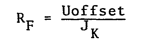
Im Zähler fällt RF heraus, wenn sich die Offset-Spannung zwischen den aufeinanderfolgenden Phasen innerhalb einer Meßperiode nicht ändert. Langzeitänderung und Temperaturdrift sind ohne Einfluß. Der im Nenner verbleibende "Fehlerwiderstand" RF ergibt einen vom Meßwert abhängigen Fehler. Bei JK · R3 = 0,5 V und UOffset = 0,5 mV ist dieser Fehler 0,1 %. Wesentlich ist, daß die Offset-Spannungsänderung und genauso eine Änderung des Verstärkungseingangsstroms ohne Einfluß auf die Meßgenauigkeit bis herab zur Temperaturdifferenz Null sind.R F drops out in the counter if the offset voltage does not change between the successive phases within a measurement period. Long-term changes and temperature drift have no influence. The "error resistance" R F remaining in the denominator results in an error dependent on the measured value. With J K · R 3 = 0.5 V and UOffset = 0.5 mV, this error is 0.1%. It is essential that the offset voltage change and also a change in the gain input current have no influence on the measuring accuracy down to the temperature difference zero.
Die Innenwiderstände der Schalter 4 und 5 sind ohne Einfluß auf die Meßgenauigkeit, da der Strom eingeprägt wird. Innenwiderstandsänderungen der Schalter 6 und 7 könnten jedoch ohne Impedanzwandler 9 zu Fehlern führen, da sie in die Integrationszeitkonstante eingehen. Der den Operationsverstärker 11a vorgeschaltete Impedanzwandler 9 ist jedoch eingangsseitig so hochohmig, daß große Widerstandsänderungen der Schalter 6 und 7 zugelassen werden können. Die Sperrströme der Schalter 4 bis 8 können vernachlässigt werden, da immer einer der Schalter 6, 7 oder 8 geschlossen ist und die Widerstände 1 bis 3 sehr niederohmig sind.The internal resistances of
Im folgenden wird nun die Funktion des Kompensationswiderstands 12 erläutert.The function of the
Ohne diesen Kompensationswiderstand 12 würde als Integrationsspannung für den Integrator 11 stets die volle am Temperaturmeßwiderstand 1 bzw. 2 anstehende Spannung wirken.Without this
Das führt dazu, daß sich die Meßzeiten, d.h. die Dauer der Phasen 2 und 4, bei einer Temperaturänderung von z.B. 20° auf 90° - entsprechend einer Widerstandsänderung von z.B. 540 Ohm auf 770 Ohm - nur etwa um 25 % ändern. Anzustreben ist aber, daß die Meßzeit an der unteren Grenze des Temperaturmeßbereichs Null wird, indem man den Widerstandswert der Temperaturmeßwiderstände an der unteren Meßbereichsgrenze, z.B. bei 0° C mit dem Widerstand 12 kompensiert.The result is that the measuring times, ie the duration of
Die Widerstände 10, 12 sind dabei so dimensioniert, daß während der Phasen 1 und 3 der Integrationsstrom bei einer Meßtemperatur von z.B. 0° Null ist. Dies wird erreicht, wenn gilt: R1/R3= R10/R12. Bei der obengenannten Temperaturänderung von 20° auf 90° ändert sich die Meßzeit nicht mehr von z.B. 100 auf 125 ms, sondern von 5 auf 30 ms. Damit wird die Dauer der gesamten Meßperiode entsprechend verkürzt, so daß auch der Stromverbrauch der Anordnung geringer wird. Dies ist wichtig, wenn die Meßanordnung mit einer Batterie betrieben wird.The
Während der Phasen 2 und 4, während derer der Schalter 8 geschlossen ist, liegt der invertierende Eingang des Operationsverstärkers 11a über den Widerstand 12 an Bezugspotential, während durch die Diode 9b der Impedanzwandler mit dem vorgeschalteten Schaltungsteil völlig vom Operationsverstärker 11a entkoppelt ist.During
Mit der beschriebenen Kompensation kann also die Meßzeit, d.h. die Dauer der Phasen 2 und 4, verkürzt werden, wobei jedoch die Meßzeitänderung bei vorgegebener Temperaturänderung und damit die Auflösung gleich bleibt. Aus Stromersparnisgründen möchte man auch die konstanten Zeiten der Phasen 1 und 3 so kurz wie möglich halten. Würde man diese konstanten Zeiten ohne weitere Maßnahmen verkürzen, so würde man entsprechend auch die Meßzeitdifferenzen und damit die Auflösung verkleinern.With the compensation described, the measuring time, i.e. the duration of
Dieses Problem kann dadurch gelöst werden, daß man entsprechend einer Anordnung nach Fig. 3 in Reihe zu dem Kompensationswiderstand 12 einen weiteren Widerstand 15 schaltet, der mit einem Schalter 16 überbrückbar ist. Der Schalter 16 wird während der Phasen 1 und 3 geschlossen, so daß nur der Kompensationswiderstand 12 für die Grundwiderstandskompensation wirksam wird. Während der Meßzeiten, d.h. während der Phasen 2 und 4, ist der Schalter 16 geöffnet, so daß die Reihenschaltung der Widerstände 12 und 15 wirksam wird. Der dadurch bedingte geringere Ladestrom für den Kondensator 11b des Integrators 11 bewirkt bei gleichlangen Phasen 1 un'' 3 eine Verlängerung der Meßzeiten, d.h. der Phasen 2 und 4. Bei gleichbleibender Auflösung können daher die Phasen 1 und 3 entsprechend verkürzt werden.This problem can be solved by connecting a
Durch die zur Verkürzung einer Meßperiode erforderlichen zusätzlichen Elemente, z.B. durch den Innenwiderstand des Schalters 16, entsteht ein Meßfehler bei der Umwandlung jeder einzelnen Meßtempratur. Bei der Differenzbildung der Meßtemperaturen fällt jedoch der Fehler weg, sofern sich die Störgrößen während einer relativ kurzen Meßperiode nicht ändern.The additional elements required to shorten a measuring period, e.g. due to the internal resistance of the
Der genannte Meßfehler würde jedoch voll in das Meßergebnis eingehen, wenn man die einzelnen Meßtemperaturen bestimmen will. Dieses Problem kann gelöst werden, wenn man die Ermittlung der einzelnen Meßtemperaturen wieder auf eine Differenzbildung zurückführt. Bei einem Ausführungsbeispiel nach Fig. 4 ist dabei ein weiterer Meßzweig mit einem konstanten Vergleichswiderstand 17 vorgesehen, der einerseits über einen Schalter 18 an die Konstantstromquelle 14 und andererseits an den Referenzwiderstand 3 angeschlossen ist. Der Verbindungspunkt von Schalter 18 und Vergleichswiderstand 17 ist über einen Schalter 19 mit dem Eingang des Impedanzwandlers 9 verbunden. Ansonsten entspricht die Schaltung dem Ausführungsbeispiel nach Fig. 3. Nach dem bereits besprochenen Verfahren wird auch die am Vergleichswiderstand 17 anstehende Spannung in einen Digitalwert umgewandelt. Die mit jedem Temperaturmeßwiderstand 1 und 2 erfaßte Meßtemperatur kann damit einzeln durch Differenzbildung mit dem so gewonnenen konstanten Wert ermittelt werden. Durch die Differenzbildung können die Absoluttemperaturen der Meßwiderstände 1 und 2 ebenso genau ermittelt werden, wie deren Differenztemperatur.However, the measurement error mentioned would be fully included in the measurement result if one wanted to determine the individual measurement temperatures. This problem can be solved if the determination of the individual measurement temperatures is traced back to a difference. 4, a further measuring branch with a
Mit den dargestellten Schaltungsmaßnahmen gelingt es also, die Dauer einer Meßperiode deutlich zu verringern, und zwar sowohl die konstanten Zeiten der Phasen 1 und 3 als auch die Meßzeiten der Phasen 2 und 4. Daiu sind nur sehr wenige und außerdem billige Bauelemente erforderlich.With the circuit measures shown it is thus possible to significantly reduce the duration of a measurement period, specifically both the constant times of
Claims (4)
Priority Applications (1)
| Application Number | Priority Date | Filing Date | Title |
|---|---|---|---|
| AT84106350T ATE26342T1 (en) | 1983-06-16 | 1984-06-04 | MEASURING DEVICE FOR DETECTING A TEMPERATURE DIFFERENCE. |
Applications Claiming Priority (2)
| Application Number | Priority Date | Filing Date | Title |
|---|---|---|---|
| DE19833321862 DE3321862A1 (en) | 1983-06-16 | 1983-06-16 | MEASURING DEVICE FOR DETECTING A TEMPERATURE DIFFERENCE |
| DE3321862 | 1983-06-16 |
Publications (2)
| Publication Number | Publication Date |
|---|---|
| EP0129132A1 true EP0129132A1 (en) | 1984-12-27 |
| EP0129132B1 EP0129132B1 (en) | 1987-04-01 |
Family
ID=6201719
Family Applications (1)
| Application Number | Title | Priority Date | Filing Date |
|---|---|---|---|
| EP84106350A Expired EP0129132B1 (en) | 1983-06-16 | 1984-06-04 | Measuring device to detect a temperature difference |
Country Status (3)
| Country | Link |
|---|---|
| EP (1) | EP0129132B1 (en) |
| AT (1) | ATE26342T1 (en) |
| DE (2) | DE3321862A1 (en) |
Cited By (2)
| Publication number | Priority date | Publication date | Assignee | Title |
|---|---|---|---|---|
| US6824308B2 (en) * | 2002-11-07 | 2004-11-30 | Omron Corporation | Temperature detecting device |
| DE102005029319A1 (en) * | 2005-06-24 | 2006-12-28 | Abb Patent Gmbh | Circuit arrangement, for determining temperature difference between two sensors, has digital microprocessor to determine temperature difference from digitized signals of analog-to-digital converter and provide temperature difference signal |
Families Citing this family (2)
| Publication number | Priority date | Publication date | Assignee | Title |
|---|---|---|---|---|
| EP0510880B1 (en) * | 1991-04-23 | 2002-07-10 | Kabushiki Kaisha Toshiba | Cryogenic measurement equipment |
| EP3935360A1 (en) * | 2019-03-08 | 2022-01-12 | Nokia Technologies Oy | Temperature detection |
Citations (3)
| Publication number | Priority date | Publication date | Assignee | Title |
|---|---|---|---|---|
| FR2305894A1 (en) * | 1975-03-26 | 1976-10-22 | Weston Instruments Inc | DIGITAL MEASUREMENT DEVICE |
| FR2377730A1 (en) * | 1977-01-12 | 1978-08-11 | Johnson & Johnson | PULSE GENERATOR CONVERTER CIRCUIT |
| US4161880A (en) * | 1978-01-05 | 1979-07-24 | Electromedics, Inc. | Linearized digital thermometer |
-
1983
- 1983-06-16 DE DE19833321862 patent/DE3321862A1/en not_active Withdrawn
-
1984
- 1984-06-04 EP EP84106350A patent/EP0129132B1/en not_active Expired
- 1984-06-04 DE DE8484106350T patent/DE3462951D1/en not_active Expired
- 1984-06-04 AT AT84106350T patent/ATE26342T1/en not_active IP Right Cessation
Patent Citations (3)
| Publication number | Priority date | Publication date | Assignee | Title |
|---|---|---|---|---|
| FR2305894A1 (en) * | 1975-03-26 | 1976-10-22 | Weston Instruments Inc | DIGITAL MEASUREMENT DEVICE |
| FR2377730A1 (en) * | 1977-01-12 | 1978-08-11 | Johnson & Johnson | PULSE GENERATOR CONVERTER CIRCUIT |
| US4161880A (en) * | 1978-01-05 | 1979-07-24 | Electromedics, Inc. | Linearized digital thermometer |
Cited By (2)
| Publication number | Priority date | Publication date | Assignee | Title |
|---|---|---|---|---|
| US6824308B2 (en) * | 2002-11-07 | 2004-11-30 | Omron Corporation | Temperature detecting device |
| DE102005029319A1 (en) * | 2005-06-24 | 2006-12-28 | Abb Patent Gmbh | Circuit arrangement, for determining temperature difference between two sensors, has digital microprocessor to determine temperature difference from digitized signals of analog-to-digital converter and provide temperature difference signal |
Also Published As
| Publication number | Publication date |
|---|---|
| ATE26342T1 (en) | 1987-04-15 |
| DE3462951D1 (en) | 1987-05-07 |
| DE3321862A1 (en) | 1984-12-20 |
| EP0129132B1 (en) | 1987-04-01 |
Similar Documents
| Publication | Publication Date | Title |
|---|---|---|
| DE2350083C2 (en) | Circuit arrangement for converting a measured value recorded by a sensor | |
| DE3422716C2 (en) | ||
| EP0528784B1 (en) | Method for the determination of a measurable quantity | |
| DE2917237C2 (en) | ||
| DE2949461A1 (en) | ELECTRONIC ENERGY MEASURING DEVICE | |
| DE3117808A1 (en) | CIRCUIT ARRANGEMENT FOR MEASURING INDUCTIVE CHANGES | |
| DE2341322A1 (en) | ARRANGEMENT FOR GENERATING A MEASUREMENT OUTPUT SIGNAL, THE LEVEL OF THE LINEAR DEPENDING ON THE SIZE OF A RESISTANCE TO BE MEASURED | |
| EP0356438B1 (en) | Process and arrangement for evaluating a measurable analog electronic quantity | |
| EP0129132B1 (en) | Measuring device to detect a temperature difference | |
| DE2300802A1 (en) | CIRCUIT ARRANGEMENT FOR POTENTIAL-FREE CURRENT MEASUREMENT | |
| EP0250028B1 (en) | Circuit device for compensation of temperature dependent and temperature independent drifts of a capacitive sensor | |
| DE2258690B2 (en) | Circuit for comparing the values of two impedances | |
| DE3706306A1 (en) | CIRCUIT TO OBTAIN A TEMPERATURE-INDEPENDENT RECTANGULAR SIGNAL FROM A MEASURING SIGNAL | |
| EP0285047A2 (en) | Circuit for shaping a measure signal into a square wave signal | |
| DE2340847A1 (en) | ANALOG-DIGITAL CONVERTER FOR SIGNALS WITH INCLINED CURVE SECTIONS | |
| DE2305204A1 (en) | SYSTEM FOR CONVERTING AN INPUT SIGNAL INTO A LOGARITHMIC VALUE | |
| DE2636000C3 (en) | Circuit arrangement for the electrical measurement of a physical variable, in particular the temperature | |
| DE2515812C3 (en) | Circuit arrangement for compensating the temperature response of field plates | |
| DE3714165C2 (en) | ||
| EP1431769B1 (en) | Circuit for determining the internal resistance of a linear lambda probe | |
| DE3332940C1 (en) | Circuit arrangement for detecting the failure time of a supply voltage | |
| AT335566B (en) | DEVICE FOR MEASURING THE PARAMETERS OF A COMPLEX RESISTANT TWO-POLE | |
| DD227257A1 (en) | ARRANGEMENT FOR STEREO SIZE COMPENSATION FOR MEASURING CONSUMERS IN BRIDGE CIRCUITS | |
| DE2416330C2 (en) | Static measuring device that can be calibrated with direct current | |
| DD274126A1 (en) | CIRCUIT ARRANGEMENT IN A DIGITAL MULTI-MEASUREMENT DEVICE |
Legal Events
| Date | Code | Title | Description |
|---|---|---|---|
| PUAI | Public reference made under article 153(3) epc to a published international application that has entered the european phase |
Free format text: ORIGINAL CODE: 0009012 |
|
| AK | Designated contracting states |
Designated state(s): AT CH DE IT LI NL |
|
| 17P | Request for examination filed |
Effective date: 19850426 |
|
| 17Q | First examination report despatched |
Effective date: 19860530 |
|
| GRAA | (expected) grant |
Free format text: ORIGINAL CODE: 0009210 |
|
| AK | Designated contracting states |
Kind code of ref document: B1 Designated state(s): AT CH DE IT LI NL |
|
| REF | Corresponds to: |
Ref document number: 26342 Country of ref document: AT Date of ref document: 19870415 Kind code of ref document: T |
|
| REF | Corresponds to: |
Ref document number: 3462951 Country of ref document: DE Date of ref document: 19870507 |
|
| ITF | It: translation for a ep patent filed |
Owner name: STUDIO JAUMANN |
|
| PLBI | Opposition filed |
Free format text: ORIGINAL CODE: 0009260 |
|
| 26 | Opposition filed |
Opponent name: SPANNER- POLLUX GMBH Effective date: 19871223 |
|
| NLR1 | Nl: opposition has been filed with the epo |
Opponent name: SPANNER- POLLUX GMBH |
|
| PLBM | Termination of opposition procedure: date of legal effect published |
Free format text: ORIGINAL CODE: 0009276 |
|
| STAA | Information on the status of an ep patent application or granted ep patent |
Free format text: STATUS: OPPOSITION PROCEDURE CLOSED |
|
| 27C | Opposition proceedings terminated |
Effective date: 19881008 |
|
| ITTA | It: last paid annual fee | ||
| NLR2 | Nl: decision of opposition | ||
| PGFP | Annual fee paid to national office [announced via postgrant information from national office to epo] |
Ref country code: AT Payment date: 19990521 Year of fee payment: 16 |
|
| PGFP | Annual fee paid to national office [announced via postgrant information from national office to epo] |
Ref country code: NL Payment date: 19990615 Year of fee payment: 16 |
|
| PGFP | Annual fee paid to national office [announced via postgrant information from national office to epo] |
Ref country code: CH Payment date: 19990920 Year of fee payment: 16 |
|
| PG25 | Lapsed in a contracting state [announced via postgrant information from national office to epo] |
Ref country code: AT Free format text: LAPSE BECAUSE OF NON-PAYMENT OF DUE FEES Effective date: 20000604 |
|
| PG25 | Lapsed in a contracting state [announced via postgrant information from national office to epo] |
Ref country code: LI Free format text: LAPSE BECAUSE OF NON-PAYMENT OF DUE FEES Effective date: 20000630 Ref country code: CH Free format text: LAPSE BECAUSE OF NON-PAYMENT OF DUE FEES Effective date: 20000630 |
|
| PG25 | Lapsed in a contracting state [announced via postgrant information from national office to epo] |
Ref country code: NL Free format text: LAPSE BECAUSE OF NON-PAYMENT OF DUE FEES Effective date: 20010101 |
|
| REG | Reference to a national code |
Ref country code: CH Ref legal event code: PL |
|
| NLV4 | Nl: lapsed or anulled due to non-payment of the annual fee |
Effective date: 20010101 |
|
| PGFP | Annual fee paid to national office [announced via postgrant information from national office to epo] |
Ref country code: DE Payment date: 20020819 Year of fee payment: 19 |
|
| PG25 | Lapsed in a contracting state [announced via postgrant information from national office to epo] |
Ref country code: DE Free format text: LAPSE BECAUSE OF NON-PAYMENT OF DUE FEES Effective date: 20040101 |