EP0122645B1 - Procédé de couplage de deux éléments optiques constituant un dispositif de transmission d'informations lumineuses, et dispositif ainsi obtenu - Google Patents
Procédé de couplage de deux éléments optiques constituant un dispositif de transmission d'informations lumineuses, et dispositif ainsi obtenu Download PDFInfo
- Publication number
- EP0122645B1 EP0122645B1 EP84200294A EP84200294A EP0122645B1 EP 0122645 B1 EP0122645 B1 EP 0122645B1 EP 84200294 A EP84200294 A EP 84200294A EP 84200294 A EP84200294 A EP 84200294A EP 0122645 B1 EP0122645 B1 EP 0122645B1
- Authority
- EP
- European Patent Office
- Prior art keywords
- beads
- fiber
- fibre
- optical
- contact pads
- Prior art date
- Legal status (The legal status is an assumption and is not a legal conclusion. Google has not performed a legal analysis and makes no representation as to the accuracy of the status listed.)
- Expired
Links
Images
Classifications
-
- G—PHYSICS
- G02—OPTICS
- G02B—OPTICAL ELEMENTS, SYSTEMS OR APPARATUS
- G02B6/00—Light guides; Structural details of arrangements comprising light guides and other optical elements, e.g. couplings
- G02B6/24—Coupling light guides
- G02B6/42—Coupling light guides with opto-electronic elements
- G02B6/4201—Packages, e.g. shape, construction, internal or external details
- G02B6/4219—Mechanical fixtures for holding or positioning the elements relative to each other in the couplings; Alignment methods for the elements, e.g. measuring or observing methods especially used therefor
- G02B6/4236—Fixing or mounting methods of the aligned elements
- G02B6/4238—Soldering
-
- G—PHYSICS
- G02—OPTICS
- G02B—OPTICAL ELEMENTS, SYSTEMS OR APPARATUS
- G02B6/00—Light guides; Structural details of arrangements comprising light guides and other optical elements, e.g. couplings
- G02B6/24—Coupling light guides
- G02B6/42—Coupling light guides with opto-electronic elements
- G02B6/4201—Packages, e.g. shape, construction, internal or external details
- G02B6/4202—Packages, e.g. shape, construction, internal or external details for coupling an active element with fibres without intermediate optical elements, e.g. fibres with plane ends, fibres with shaped ends, bundles
Definitions
- the present invention relates to a method of coupling a first optical element consisting of an optical fiber with respect to a second optical element, comprising an optoelectronic component carrying at least one junction created in a semiconductor body and whose contact sockets are formed of metal pads arranged on the surface of the various semiconductor regions of said body, method according to which the active face of one end of said fiber is brought opposite the second element in a position such that the transfer efficiency of the light radiation transmitted by said fiber is optimal, the assembly being maintained in this position until it is coated in an opaque plastic material forming an envelope impervious to external light radiation, the assembly thus formed constituting a device for transmitting light information.
- the present invention also relates to the device obtained by this method.
- optical fibers which can be used in high frequency ranges, have the advantage of being insensitive to external parasitic disturbances and have a lower attenuation coefficient than conventional coaxial cables.
- the diameter of the active section of an optical fiber is currently stabilized around 50 gm.
- a type of fiber is generally associated with electronic components, in particular sources. emitting light, created on semiconductor crystals whose photoactive junction has a diameter of substantially equivalent dimension.
- knowing that the acceptance angle of an optical fiber may not exceed 10 ° it is obvious that if the emissive source is not sufficiently directive or if the active face of the fiber, it is that is to say the face opposite the semiconductor junction, is not put in place with precision, the transfer or coupling efficiency is notably reduced.
- the photoreceptor element is generally a semiconductor diode whose junction diameter is greater than that of the section of the active face of the fiber, which allows a certain margin of error in the setting place and centering of the elements.
- the surface of the photoreceptive diode relative to that of the fiber section, we encounter the same difficulties as in the case more widely explained above of centering a fiber with respect to to an emissive source.
- the optoelectronic components or end components, are often attached to a fiber called information transfer fiber via a short fiber, called fiber primer, permanently attached to each of said components.
- This solution which is advantageous from an industrial point of view, also requires perfect centering of the seed fiber with respect to the optoelectronic component.
- the fiber transmission devices comprise at each of its ends an optoelectronic component carried by a metal support and encased in an opaque plastic envelope.
- an optoelectronic component carried by a metal support and encased in an opaque plastic envelope.
- a conduit is formed in which is introduced and fixed one end of the transfer fiber or of the pigtail.
- a commonly used method consists in using a semiconductor diode called "Bur- in the cavity of which the end of the optical fiber is introduced, the active face of which is applied to the bottom of said cavity.
- Japanese patent application JP-A-5 753 989 discloses a coupler for a light-emitting diode to an optical fiber, of the type using a transparent ball. The latter is held in position before coating by a curved part of the connection wires. This positioning is imprecise because of the elasticity of the wires and also has the drawback of introducing permanent stressing of the latter.
- the present invention aims to remedy these drawbacks. To do this, it relies on the fact that the best way to obtain a high light transfer between an optical fiber and an optoelectronic component is to apply the active face located at the end of said fiber as close as possible to the junction. semiconductor of said component, and it is also based on the progress made in the techniques of localized metallic deposits usually used in the semiconductor industry such as transistors or integrated circuits.
- the present invention relates to a coupling method of the aforementioned type and which is particularly remarkable in that, during thermocompression welding of connection wires on the metallic contact pads, there are at least three pads on them. partially spherical shape and of cross section greater than that of said wires, said studs being arranged in such a way that they are tangential to the periphery of a circular domain of diameter equal to that of optical fiber, in that one slides the end of the latter between said studs so as to apply the active face against the metal contact pads of the optoelectronic component as close as possible to the surface of the optoelectronic component, and in that said end of the fiber in this position before coating the assembly in the opaque plastic material constituting the protective envelope.
- connection wires on the metal contact pads can be carried out without the need for additional operations and / or special equipment. It will be advantageous, for example, to carry out the welding of the connection wires on the metal contact pads by a thermocompression process known to specialists under the name of "nail head welding".
- the principle of this welding process consists, in fact, in lowering and pressing on the metal contact pads the end of a wire to which the shape of a ball has previously been given and which, after pressing, takes the shape of a bulging stud. Under these conditions, the welding of the connection wires and the production of the partially spherical studs in accordance with the present invention are simultaneously obtained.
- the studs being substantially spherical, the guiding of the fiber is favored by the rounded contours which form a funnel.
- the use of the equipment adapted to this welding process makes it possible to benefit, moreover, from its own advantages, namely precision in the placement of the pads (resolution of the order of 4 (jLm). pads deposited per second), automation of the deposit operation from precise programming obtained manually.
- the metal contact pads and the pads which cover them are advantageously at least four in number.
- the implementation of the method according to the invention applies to all types of optical fiber transmission devices, but it is particularly advantageous in the case of devices to be removed from said lateral fiber. It is known, in fact, that fiber transmission devices are most often fixed on printed circuits carried by plug-in cards arranged parallel to each other and between which space is limited. It is therefore preferable that the optical fiber leaving each of the devices is oriented in a direction parallel to the plane of said cards and not in a perpendicular direction.
- the present invention also relates to the device for transmitting light information obtained by the method described above and comprising in particular two optical elements, the first of which consists of at least one optical fiber and the second element of which essentially comprises an optoelectronic component created in a semiconductor body and the contact points of which are formed of surface metal layers, the two optical elements being held and encased in an opaque plastic material, a device notably remarkable in that the end of the optical fiber is clamped between at least three partially spherical metal studs deposited on the surface of the contact pads of the device.
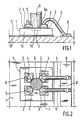
- FIG. 1 represents a very diagrammatic front view of the device for transmitting light information obtained by the method according to the invention.
- FIG. 2 represents a top view of this same device.
- these studs are obtained by crushing a ball previously formed at the end of the connection wire.
- Said metal studs 4 are therefore intended to circumscribe an area where the optical fiber 6 is easily accommodated on the same axis and as close as possible to the junction J, taking support by its active face 6a on the pads 2 and 3, and guided by said studs 4.
- the second purpose of said studs is to allow the making of the contact with the outside of regions 1a and 1b of the semiconductor crystal 1 via the metal pads 2 and 3, and of metallic layers such as layer 9 deposited on the support. insulator 8.
- the number of metal studs 4 is at least chosen to be equal to four so that, in the event that the location of one of them relative to the intended location is slightly offset, the fiber 6 is however guided by more than two support points.
- the assembly consisting of the semiconductor crystal (1), the metal pads (2, 3), the pads (4), the wires (5) and the end of the fiber (6) is then coated in a protective envelope. opaque plastic material not shown in the figure.
Landscapes
- Physics & Mathematics (AREA)
- General Physics & Mathematics (AREA)
- Optics & Photonics (AREA)
- Optical Couplings Of Light Guides (AREA)
Applications Claiming Priority (2)
| Application Number | Priority Date | Filing Date | Title |
|---|---|---|---|
| FR8303418 | 1983-03-02 | ||
| FR8303418A FR2542100B1 (fr) | 1983-03-02 | 1983-03-02 | Procede de couplage de deux elements optiques constituant un dispositif de transmission d'informations lumineuses, et dispositif ainsi obtenu |
Publications (2)
| Publication Number | Publication Date |
|---|---|
| EP0122645A1 EP0122645A1 (fr) | 1984-10-24 |
| EP0122645B1 true EP0122645B1 (fr) | 1988-09-07 |
Family
ID=9286425
Family Applications (1)
| Application Number | Title | Priority Date | Filing Date |
|---|---|---|---|
| EP84200294A Expired EP0122645B1 (fr) | 1983-03-02 | 1984-03-01 | Procédé de couplage de deux éléments optiques constituant un dispositif de transmission d'informations lumineuses, et dispositif ainsi obtenu |
Country Status (5)
| Country | Link |
|---|---|
| US (1) | US4632504A (cg-RX-API-DMAC7.html) |
| EP (1) | EP0122645B1 (cg-RX-API-DMAC7.html) |
| JP (1) | JPS59166909A (cg-RX-API-DMAC7.html) |
| DE (1) | DE3473940D1 (cg-RX-API-DMAC7.html) |
| FR (1) | FR2542100B1 (cg-RX-API-DMAC7.html) |
Families Citing this family (2)
| Publication number | Priority date | Publication date | Assignee | Title |
|---|---|---|---|---|
| US4768070A (en) * | 1986-03-20 | 1988-08-30 | Hitachi, Ltd | Optoelectronics device |
| US5397892A (en) * | 1994-01-07 | 1995-03-14 | Coltene/Whaledent, Inc. | Fiber optic light source for a dental curing lamp with two pegs for removably aligning the source with an intensity detector |
Family Cites Families (7)
| Publication number | Priority date | Publication date | Assignee | Title |
|---|---|---|---|---|
| US4017962A (en) * | 1975-06-27 | 1977-04-19 | General Dynamics Corporation | Integrated array of optical fibers and thin film optical detectors, and method for fabricating the same |
| FR2387517A1 (fr) * | 1977-04-13 | 1978-11-10 | Thomson Csf | Systeme d'encapsulation etanche d'un dispositif optoelectronique emetteur ou recepteur a transmission par fibre optique |
| US4184070A (en) * | 1977-12-23 | 1980-01-15 | Texas Instruments Incorporated | Connector apparatus |
| JPS5522713A (en) * | 1978-08-04 | 1980-02-18 | Fujitsu Ltd | Connector mechanism of photo semiconductor device |
| FR2446497A1 (fr) * | 1979-01-09 | 1980-08-08 | Thomson Csf | Tete de couplage opto-electronique et procede de montage d'une telle tete |
| JPS6060043B2 (ja) * | 1979-02-09 | 1985-12-27 | 富士通株式会社 | 光半導体パッケ−ジ |
| JPS56113111A (en) * | 1980-02-13 | 1981-09-05 | Hitachi Ltd | Light emission element package provided with optical fiber |
-
1983
- 1983-03-02 FR FR8303418A patent/FR2542100B1/fr not_active Expired
-
1984
- 1984-02-17 US US06/581,483 patent/US4632504A/en not_active Expired - Fee Related
- 1984-02-28 JP JP59035476A patent/JPS59166909A/ja active Granted
- 1984-03-01 DE DE8484200294T patent/DE3473940D1/de not_active Expired
- 1984-03-01 EP EP84200294A patent/EP0122645B1/fr not_active Expired
Also Published As
| Publication number | Publication date |
|---|---|
| FR2542100B1 (fr) | 1985-06-07 |
| EP0122645A1 (fr) | 1984-10-24 |
| JPS59166909A (ja) | 1984-09-20 |
| JPH0336404B2 (cg-RX-API-DMAC7.html) | 1991-05-31 |
| US4632504A (en) | 1986-12-30 |
| DE3473940D1 (en) | 1988-10-13 |
| FR2542100A1 (fr) | 1984-09-07 |
Similar Documents
| Publication | Publication Date | Title |
|---|---|---|
| EP3610309B1 (fr) | Puce photonique à structure de collimation intégrée | |
| US6932522B2 (en) | Method and apparatus for hermetically sealing photonic devices | |
| EP0637764B1 (fr) | Procédé de fabrication d'une structure de couplage optique intégrante un guide optique clivé à un support de fibre optique | |
| JP3150662B2 (ja) | 金属蒸着された光繊維アレイモジュール | |
| EP1269238B1 (fr) | Procede et dispositif d'alignement passif de fibres optiques et de composants optoelectroniques | |
| FR3066617A1 (fr) | Puce photonique a structure reflechissante de repliement de trajet optique | |
| EP0860724A1 (fr) | Procédé d'assemblage d'un dispositif opto-hybride | |
| KR100248054B1 (ko) | 솔더링을 이용한 광섬유어레이 모듈 및 그 제작방법 | |
| EP3538937B1 (fr) | Procédé de réalisation collective d'une pluralité de puces optoélectroniques | |
| FR3075466A1 (fr) | Couvercle de boitier de circuit electronique | |
| EP0122645B1 (fr) | Procédé de couplage de deux éléments optiques constituant un dispositif de transmission d'informations lumineuses, et dispositif ainsi obtenu | |
| EP0498700B1 (fr) | Procédé de fabrication d'un dispositif optoélectronique | |
| EP0176154B1 (fr) | Procédé de fabrication d'un composant d'éxtrémite pour fibre optique, et composant ainsi obtenu | |
| US7057255B2 (en) | Photodiode, optical receiver device including the same, and method of making the photodiode | |
| FR2464491A1 (fr) | Module de couplage optique applique a un dispositif optoelectronique a montage plan et procede de realisation du couplage | |
| EP0520952A1 (fr) | Procédé pour coupler une fibre optique à un composant optoélectronique et dispositif de raccordement obtenus | |
| EP3812811B1 (fr) | Procédé de fabrication d'une puce photonique par report d'une vignette sur un substrat de réception | |
| FR2533710A1 (fr) | Procede d'assemblage d'un dispositif de transmission par fibre optique | |
| EP0004800B1 (fr) | Matrice pour convertisseur opto-électronique et convertisseur pour extrémité de câbles à fibres optiques | |
| JP3997915B2 (ja) | 光モジュール、光コネクタフェルール、及びこれらの製造方法 | |
| EP1624493A2 (fr) | Procédé de fabrication de module optique pour boîtier semiconducteur à capteur optique | |
| JP3107155B2 (ja) | 半導体レーザモジュール | |
| FR3075991A1 (fr) | Procede de fabrication de structures de couplage et d'alignement d'une fibre optique | |
| FR2698453A1 (fr) | Procédé de couplage d'une fibre optique avec un composant optoélectronique et dispositif de couplage. | |
| FR3030785A1 (fr) | Systeme de transmission d'une lumiere laser a travers une paroi comprenant un cordon pour evacuer des modes de gaine et procede de fabrication correspondant |
Legal Events
| Date | Code | Title | Description |
|---|---|---|---|
| PUAI | Public reference made under article 153(3) epc to a published international application that has entered the european phase |
Free format text: ORIGINAL CODE: 0009012 |
|
| AK | Designated contracting states |
Designated state(s): DE FR GB SE |
|
| 17P | Request for examination filed |
Effective date: 19841219 |
|
| 17Q | First examination report despatched |
Effective date: 19860507 |
|
| RAP1 | Party data changed (applicant data changed or rights of an application transferred) |
Owner name: N.V. PHILIPS' GLOEILAMPENFABRIEKEN Owner name: RTC-COMPELEC |
|
| GRAA | (expected) grant |
Free format text: ORIGINAL CODE: 0009210 |
|
| AK | Designated contracting states |
Kind code of ref document: B1 Designated state(s): DE FR GB SE |
|
| REF | Corresponds to: |
Ref document number: 3473940 Country of ref document: DE Date of ref document: 19881013 |
|
| GBT | Gb: translation of ep patent filed (gb section 77(6)(a)/1977) | ||
| PLBE | No opposition filed within time limit |
Free format text: ORIGINAL CODE: 0009261 |
|
| STAA | Information on the status of an ep patent application or granted ep patent |
Free format text: STATUS: NO OPPOSITION FILED WITHIN TIME LIMIT |
|
| 26N | No opposition filed | ||
| REG | Reference to a national code |
Ref country code: FR Ref legal event code: CA |
|
| REG | Reference to a national code |
Ref country code: FR Ref legal event code: CD |
|
| EAL | Se: european patent in force in sweden |
Ref document number: 84200294.1 |
|
| PGFP | Annual fee paid to national office [announced via postgrant information from national office to epo] |
Ref country code: GB Payment date: 19960229 Year of fee payment: 13 |
|
| PGFP | Annual fee paid to national office [announced via postgrant information from national office to epo] |
Ref country code: SE Payment date: 19960326 Year of fee payment: 13 |
|
| PGFP | Annual fee paid to national office [announced via postgrant information from national office to epo] |
Ref country code: FR Payment date: 19960327 Year of fee payment: 13 |
|
| PGFP | Annual fee paid to national office [announced via postgrant information from national office to epo] |
Ref country code: DE Payment date: 19960523 Year of fee payment: 13 |
|
| REG | Reference to a national code |
Ref country code: FR Ref legal event code: CD |
|
| PG25 | Lapsed in a contracting state [announced via postgrant information from national office to epo] |
Ref country code: GB Effective date: 19970301 |
|
| PG25 | Lapsed in a contracting state [announced via postgrant information from national office to epo] |
Ref country code: SE Effective date: 19970302 |
|
| GBPC | Gb: european patent ceased through non-payment of renewal fee |
Effective date: 19970301 |
|
| PG25 | Lapsed in a contracting state [announced via postgrant information from national office to epo] |
Ref country code: FR Free format text: LAPSE BECAUSE OF NON-PAYMENT OF DUE FEES Effective date: 19971128 |
|
| PG25 | Lapsed in a contracting state [announced via postgrant information from national office to epo] |
Ref country code: DE Effective date: 19971202 |
|
| EUG | Se: european patent has lapsed |
Ref document number: 84200294.1 |
|
| REG | Reference to a national code |
Ref country code: FR Ref legal event code: ST |