EP0118537B1 - Herstellungsverfahren von mikrowellenrillenelementen - Google Patents
Herstellungsverfahren von mikrowellenrillenelementen Download PDFInfo
- Publication number
- EP0118537B1 EP0118537B1 EP83902975A EP83902975A EP0118537B1 EP 0118537 B1 EP0118537 B1 EP 0118537B1 EP 83902975 A EP83902975 A EP 83902975A EP 83902975 A EP83902975 A EP 83902975A EP 0118537 B1 EP0118537 B1 EP 0118537B1
- Authority
- EP
- European Patent Office
- Prior art keywords
- mandrel
- billet
- clamping
- clamping means
- layers
- Prior art date
- Legal status (The legal status is an assumption and is not a legal conclusion. Google has not performed a legal analysis and makes no representation as to the accuracy of the status listed.)
- Expired
Links
Images

Classifications
-
- H—ELECTRICITY
- H01—ELECTRIC ELEMENTS
- H01Q—ANTENNAS, i.e. RADIO AERIALS
- H01Q13/00—Waveguide horns or mouths; Slot antennas; Leaky-waveguide antennas; Equivalent structures causing radiation along the transmission path of a guided wave
- H01Q13/02—Waveguide horns
- H01Q13/0283—Apparatus or processes specially provided for manufacturing horns
- H01Q13/0291—Apparatus or processes specially provided for manufacturing horns for corrugated horns
-
- H—ELECTRICITY
- H01—ELECTRIC ELEMENTS
- H01P—WAVEGUIDES; RESONATORS, LINES, OR OTHER DEVICES OF THE WAVEGUIDE TYPE
- H01P11/00—Apparatus or processes specially adapted for manufacturing waveguides or resonators, lines, or other devices of the waveguide type
- H01P11/001—Manufacturing waveguides or transmission lines of the waveguide type
- H01P11/002—Manufacturing hollow waveguides
-
- Y—GENERAL TAGGING OF NEW TECHNOLOGICAL DEVELOPMENTS; GENERAL TAGGING OF CROSS-SECTIONAL TECHNOLOGIES SPANNING OVER SEVERAL SECTIONS OF THE IPC; TECHNICAL SUBJECTS COVERED BY FORMER USPC CROSS-REFERENCE ART COLLECTIONS [XRACs] AND DIGESTS
- Y10—TECHNICAL SUBJECTS COVERED BY FORMER USPC
- Y10S—TECHNICAL SUBJECTS COVERED BY FORMER USPC CROSS-REFERENCE ART COLLECTIONS [XRACs] AND DIGESTS
- Y10S29/00—Metal working
- Y10S29/012—Method or apparatus with electroplating
-
- Y—GENERAL TAGGING OF NEW TECHNOLOGICAL DEVELOPMENTS; GENERAL TAGGING OF CROSS-SECTIONAL TECHNOLOGIES SPANNING OVER SEVERAL SECTIONS OF THE IPC; TECHNICAL SUBJECTS COVERED BY FORMER USPC CROSS-REFERENCE ART COLLECTIONS [XRACs] AND DIGESTS
- Y10—TECHNICAL SUBJECTS COVERED BY FORMER USPC
- Y10S—TECHNICAL SUBJECTS COVERED BY FORMER USPC CROSS-REFERENCE ART COLLECTIONS [XRACs] AND DIGESTS
- Y10S29/00—Metal working
- Y10S29/026—Method or apparatus with machining
-
- Y—GENERAL TAGGING OF NEW TECHNOLOGICAL DEVELOPMENTS; GENERAL TAGGING OF CROSS-SECTIONAL TECHNOLOGIES SPANNING OVER SEVERAL SECTIONS OF THE IPC; TECHNICAL SUBJECTS COVERED BY FORMER USPC CROSS-REFERENCE ART COLLECTIONS [XRACs] AND DIGESTS
- Y10—TECHNICAL SUBJECTS COVERED BY FORMER USPC
- Y10T—TECHNICAL SUBJECTS COVERED BY FORMER US CLASSIFICATION
- Y10T29/00—Metal working
- Y10T29/49—Method of mechanical manufacture
- Y10T29/49002—Electrical device making
- Y10T29/49016—Antenna or wave energy "plumbing" making
-
- Y—GENERAL TAGGING OF NEW TECHNOLOGICAL DEVELOPMENTS; GENERAL TAGGING OF CROSS-SECTIONAL TECHNOLOGIES SPANNING OVER SEVERAL SECTIONS OF THE IPC; TECHNICAL SUBJECTS COVERED BY FORMER USPC CROSS-REFERENCE ART COLLECTIONS [XRACs] AND DIGESTS
- Y10—TECHNICAL SUBJECTS COVERED BY FORMER USPC
- Y10T—TECHNICAL SUBJECTS COVERED BY FORMER US CLASSIFICATION
- Y10T29/00—Metal working
- Y10T29/49—Method of mechanical manufacture
- Y10T29/49826—Assembling or joining
- Y10T29/49861—Sizing mating parts during final positional association
Definitions
- This invention relates to the fabrication of microwave components and specifically to the fabrication of corrugated or ridged microwave components.
- Corrugated or ridged feeds, horns, waveguide sections, filters and other devices are useful in a wide variety of microwave applications. These corrugated devices are difficult to fabricate with accuracy and the higher their frequency of operation, the more difficult it is to obtain the required accuracy. Atfrequencies exceeding approximately 10 GHz, dimension control of fins, fin spacing and wall thicknesses become difficult and costly. Furthermore, weight of the microwave device becomes a factor of importance in certafn_applications, such as in satellite communications.
- a prior art method for fabricating corrugated horns was electroforming on a mandrel.
- the mandrel would have the desired taper and slots for fins and afterthe electroforming of the device onto the mandrel was completed, the mandrel would be removed by chemical etching.
- This method is in many cases satisfactory for operational frequencies lower than approximately 10 GHz. Above that frequency, accurate fin thickness is difficult to obtain in the mandrel due to the small size of the fins. Also the fin depth is restricted since structurally, the mandrel could only be slotted to a certain depth. Due to these mechanical restrictions, the fin width to depth ratio is limited and this limits the maximum frequency of operation. Since the mandrel was chemically etched away it is not reusable thus adding to the cost of fabrication. Also, the etching process can be lengthy which adds to the cost and lessens the ease of manufacture.
- a second method of fabrication used in the prior art is casting. This method has found little application in the higher frequency ranges since required accuracy is extremely difficult or impossible to obtain. Above approximately 10 GHz, it is extremely difficult to obtain the small fin width required. Also, casting molds are relatively expensive.
- a horn operable as high as 100 GHz may be constructed using Dragone's process, (pag6 887) there are several disadvantages. Because the outside surface is formed and plated first, this plating must be strong enough to support the subsequent machining of the inside surface. Thus a relatively thick plating is necessary, which increases both the weight and size of the corrugated horn. Also, using Dragone's process, horn throat sections, flanges or transitions must be internally machined at the same time as the inner surface. This technique becomes physically difficult or impracticable at frequencies above approximately 20 GHz due to very small apertures and required very close tolerances.
- This method comprises the steps of shaping flanges of metal, shaping centrally apertured spacers, assembling said flanges and spacers alternately to form a stack, capping the ends of said stack, clamping the capped stack together to present a continuous outer surface, plating a continuous layer of the metal to comprise said structure on said outer surface, removing the capping from said structure and etching the metal of said spacers from the interior of the structure.
- corrugated microwave components are fabricated in accordance with the basic steps as set forth in claim 1.
- a set of plates of predetermined thickness separated by spacers of predetermined thickness is clamped together.
- This sandwich billet has the inside surface, which will be the depth of the fins of the microwave component, formed in it.
- a mandrel is formed with the same taper as the inside surface and is inserted into that surface in order to provide disk clamping and support for subsequent fabrication steps.
- Preconstructed components such as flanges, transition sections, etc. may be added to the billet as desired.
- the outside surface of the microwave component is then formed to the desired contour.
- the contoured billet with the added preconstructed components, if any, is then plated on the outside to the desired plating wall thickness.
- the mandrel is constructed so that it prevents plating from reaching the inside surface. After plating, the mandrel is removed and the spacers are chemically etched away leaving the complete corrugated microwave component.
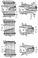
- FIG. 1 there is shown a block assembly or sandwich billet which consists of alternating materials clamped together.
- plates 10 are sandwiched next to spacers 20.
- Any suitable material may be chosen for the plates 10 including copper, brass, gold, silver, etc. and they may be in any shape depending upon manufacturing conveniences. Disks are used here for convenience of explanation.
- the thickness of disks 10 will be the fin thickness and the thickness of spacers 20 will determine the fin spacing after these spacers are later removed.
- the material of the spacers is arbitrary, however, it should be of a material which can easily be removed with chemical etching, such as aluminum, as will be further discussed later.
- Rods 30 with nuts 31 clamp the sandwiched materials together in order to support subsequent fabrication steps. Other clamping methods known in the art may be substituted for rods 30 and nuts 31.
- an inside surface 40 is formed into the billet.
- This inside surface defines the spacing between the tops of the fins and its dimensions are chosen in accordance with required electrical performance.
- a tapered surface is shown in FIG. 2; however the degree of taper, if any, is likewise in accordance with required electrical performance.
- This surface may be fabricated by installing the billet in a lathe and machining this inside surface.
- the use of a lathe and the method of forming the surface by machining are used here for explanation only: other methods known in the art such as broaching may be used to fabricate inside surface 40. Machining is used here since it is known that very accurate dimension control may be obtained through its use.
- an inside surface could have been formed in the individual plates and spacers before sandwiching. In that case, only a shaping of that surface may be required later.
- a mandrel 50 is then fabricated by machining or other suitable method and has the same taper and size as inside surface 40. This mandrel 50 is then inserted into inside surface 40 as shown in FIG. 3.
- the purpose of the mandrel 50 is to provide disk clamping support for subsequent fabrication steps. Clamp 51 and the taper of the mandrel 50 clamp the billet together.
- the mandrel 50 has a second purpose relevant to the subsequent plating step.
- the mandrel prevents the plating of inside surface 40.
- This mandrel is reusable and can be made of any suitable material such as stainless steel, aluminum, etc. Because it is reusable, manufacturing costs are correspondingly lowered and repeatability of results is correspondingly raised.
- flange 52 and throat section 53 have been added to the billet. They may be temporarily secured in place to the billet by clamp 51 which is threaded into mandrel 50. Other methods known in the art may be used to secure flange 52 to the billet.
- clamp 51 which is threaded into mandrel 50.
- Other methods known in the art may be used to secure flange 52 to the billet.
- outside surface 55 is formed.
- the contour of this surface determines fin depth, operation frequency, and other electrical parameters.
- a matching section 70 with associated greater fin depth may be fabricated. The contouring of this section 70 would occur in this step.
- outer surface 55 is plated to the desired plating wall thickness 60.
- Electroforming a copper plating is one method and one material which will accomplish this step. Other materials may be plated onto outer surface 55 such as gold, silver, nickel, etc. In addition, multiple layers of plating of different materials may be applied such as a first layer of copper and a second layer of nickel to add strength. Because of the invention, this plating 60 can be kept to a small thickness. The environmental requirements of the application such as shock, vibration, etc. will determine the actual thickness of the plating along with strength necessary to support the fins 10. In the Dragone process, this plating wall 60 must be thick enough to also support a subsequent step of machining the inside surface.
- the thickness required to support this machining step causes a much thicker wall than one obtained by use of the invention. This added thickness increases both the weight and the size of the product. In satellite, missile and many other applications, both weight and size can be of critical importance. As another example, where the end product is a waveguide horn and it is to be used in a planar array antenna with possibly 100 other identical horns, minimum weight and size are desired characteristics.
- FIG. 6 it is also shown that an additional component, if any, is also plated 61 along with outside surface 55, thus resulting in an integrated assembly.
- flange 52 with throat section 53 have been integrated.
- the invention solves the previously discussed prior art problem of difficult or impractical internal machining of such throat sections for high frequency devices.
- the formation of the throat section 53 was accomplished before it was integrated with the horn section.
- matching sections and other transition sections may be preformed before integration.
- FIG. 7 it is shown that the mandrel 50 has been removed and spacers 20 have been removed.
- the spacers 20 have been chemically etched away in order to remove them thus leaving the completed horn.
- FIG. 8 also there is shown a completed horn with a matching section 70 formed by contouring the outside surface 55 as previously discussed.
- the angle of section 70 and its dimensions vary as dictated by performance requirements.
- FIG. 9 presents an assembly of a horn structure fabricated in accordance with the invention, having fins 10, plated surface 60 and a matching section 70.
- the horn structure is connected to flange 80.
- the invention is applicable to a variety of microwave devices where corrugation is desired.
- corrugated filters, phase shifters and waveguide sections along with the example used above, the horn structure may all be fabricated with use of the invention.
- a corrugated waveguide filter fabricated in accordance with the invention is presented in FIG. 10. It, likewise, has fins 10', outside surface 55', plating 60' and two integrated flanges 81. It should be noted that a mandrel differing in shape from that shown previously would be required to fabricate this embodiment.
- a microwave horn with an integrated transition section and flange similar to that shown in FIG. 9 was constructed.
- the frequency of operation was 94 GHz and the embodiment operated successful ly.
Landscapes
- Engineering & Computer Science (AREA)
- Manufacturing & Machinery (AREA)
- Waveguide Aerials (AREA)
- Machines For Manufacturing Corrugated Board In Mechanical Paper-Making Processes (AREA)
- Control Of Motors That Do Not Use Commutators (AREA)
- Laminated Bodies (AREA)
Claims (3)
Applications Claiming Priority (2)
| Application Number | Priority Date | Filing Date | Title |
|---|---|---|---|
| US06/414,222 US4492020A (en) | 1982-09-02 | 1982-09-02 | Method for fabricating corrugated microwave components |
| US414222 | 1982-09-02 |
Publications (2)
| Publication Number | Publication Date |
|---|---|
| EP0118537A1 EP0118537A1 (de) | 1984-09-19 |
| EP0118537B1 true EP0118537B1 (de) | 1989-03-08 |
Family
ID=23640501
Family Applications (1)
| Application Number | Title | Priority Date | Filing Date |
|---|---|---|---|
| EP83902975A Expired EP0118537B1 (de) | 1982-09-02 | 1983-09-01 | Herstellungsverfahren von mikrowellenrillenelementen |
Country Status (10)
| Country | Link |
|---|---|
| US (1) | US4492020A (de) |
| EP (1) | EP0118537B1 (de) |
| JP (1) | JPS59501570A (de) |
| AU (1) | AU567439B2 (de) |
| CA (1) | CA1221227A (de) |
| DE (1) | DE3379368D1 (de) |
| DK (1) | DK209084D0 (de) |
| IT (1) | IT1171859B (de) |
| NO (1) | NO841724L (de) |
| WO (1) | WO1984001058A1 (de) |
Families Citing this family (6)
| Publication number | Priority date | Publication date | Assignee | Title |
|---|---|---|---|---|
| US6232853B1 (en) | 1999-03-12 | 2001-05-15 | Com Dev Limited | Waveguide filter having asymmetrically corrugated resonators |
| US6169466B1 (en) | 1999-05-10 | 2001-01-02 | Com Dev Limited | Corrugated waveguide filter having coupled resonator cavities |
| DE112009005487A5 (de) * | 2009-12-29 | 2012-10-04 | Werner Suedes | Verfahren zur Herstellung eines Verbundkörpers mit einer freitragenden Fläche |
| EP2649681B1 (de) | 2010-12-07 | 2015-12-30 | Ecole Polytechnique Fédérale de Lausanne (EPFL) | Geriffelte komponenten für millimeter-, submillimeter- und terahertz wellen |
| CH706053B1 (fr) | 2010-12-09 | 2017-08-15 | Ecole Polytechnique Fed De Lausanne (Epfl) | Composants passifs pour ondes électromagnétiques ayant des fréquences allant de 30 GHz à 100 THz réalisés par empilement de couches successives de matériau. |
| CN103441319A (zh) * | 2013-07-22 | 2013-12-11 | 电子科技大学 | 90g准光辐射器波纹波导设计方法 |
Family Cites Families (23)
| Publication number | Priority date | Publication date | Assignee | Title |
|---|---|---|---|---|
| US2793989A (en) * | 1952-10-02 | 1957-05-28 | Gar Prec Parts Inc | Wave guide structure and method of forming same |
| US2785382A (en) * | 1953-04-02 | 1957-03-12 | Coop Ind Inc | Flexible wave guide |
| US2761828A (en) * | 1954-08-16 | 1956-09-04 | Univ Leland Stanford Junior | Method of forming internally flanged structures |
| US2872650A (en) * | 1956-02-16 | 1959-02-03 | Monogram Prec Ind Inc | Waveguide |
| US3070873A (en) * | 1956-11-01 | 1963-01-01 | Applied Radiation Corp | Waveguide construction |
| US3103454A (en) * | 1957-10-01 | 1963-09-10 | Paocsssl | |
| NL103711C (de) * | 1959-02-10 | |||
| FR1235454A (fr) * | 1959-05-27 | 1960-07-08 | Csf | Procédé de fabrication de lignes à retard pour ondes millimétriques |
| US3192609A (en) * | 1961-02-27 | 1965-07-06 | Shin Mitsubishi Jukogyo Kk | Method of manufacturing hollow cylindrical members with apertured internal partitions |
| US3261078A (en) * | 1962-08-09 | 1966-07-19 | Bendix Corp | Method of manufacture of waveguide components |
| US3327371A (en) * | 1963-03-11 | 1967-06-27 | Bell Telephone Labor Inc | Method and apparatus for fabricating slow-wave structures |
| NL6517040A (de) * | 1965-12-28 | 1967-06-29 | ||
| US3772619A (en) * | 1971-06-04 | 1973-11-13 | Andrew Corp | Low-loss waveguide transmission |
| US3845422A (en) * | 1973-04-17 | 1974-10-29 | Microwave Dev Labor | Stop band filter |
| US3969814A (en) * | 1975-01-15 | 1976-07-20 | Trw Inc. | Method of fabricating waveguide structures |
| JPS5831398B2 (ja) * | 1977-07-13 | 1983-07-05 | 三菱電機株式会社 | コルゲ−ト導波管の製造方法 |
| FR2414256A1 (fr) * | 1978-01-06 | 1979-08-03 | Thomson Csf | Procede de realisation de charges pour ondes radioelectriques hyperfrequence |
| DE2817217A1 (de) * | 1978-04-20 | 1979-10-31 | Trumpf Maschinen Ag | Werkzeugmaschine |
| DE2947245A1 (de) * | 1979-11-23 | 1981-06-04 | Kabel- und Metallwerke Gutehoffnungshütte AG, 3000 Hannover | Verfahren zur herstellung von hohlleitern |
| DE2947246A1 (de) * | 1979-11-23 | 1981-05-27 | Kabel- und Metallwerke Gutehoffnungshütte AG, 3000 Hannover | Verfahren zur herstellung von rechteck- bzw. quadrathohlleitern |
| JPS56168402A (en) * | 1980-05-29 | 1981-12-24 | Nippon Telegr & Teleph Corp <Ntt> | Corrugated horn |
| JPS56168403A (en) * | 1980-05-29 | 1981-12-24 | Nippon Telegr & Teleph Corp <Ntt> | Corrugated horn |
| US4408208A (en) * | 1981-03-23 | 1983-10-04 | Rockwell International Corporation | Dip brazed corrugated feed horn |
-
1982
- 1982-09-02 US US06/414,222 patent/US4492020A/en not_active Expired - Lifetime
-
1983
- 1983-08-31 IT IT48903/83A patent/IT1171859B/it active
- 1983-09-01 WO PCT/US1983/001371 patent/WO1984001058A1/en active IP Right Grant
- 1983-09-01 JP JP58503041A patent/JPS59501570A/ja active Granted
- 1983-09-01 EP EP83902975A patent/EP0118537B1/de not_active Expired
- 1983-09-01 CA CA000435847A patent/CA1221227A/en not_active Expired
- 1983-09-01 DE DE8383902975T patent/DE3379368D1/de not_active Expired
- 1983-09-01 AU AU20316/83A patent/AU567439B2/en not_active Ceased
-
1984
- 1984-04-26 DK DK2090/84A patent/DK209084D0/da not_active Application Discontinuation
- 1984-04-30 NO NO841724A patent/NO841724L/no unknown
Also Published As
| Publication number | Publication date |
|---|---|
| DK209084A (da) | 1984-04-26 |
| WO1984001058A1 (en) | 1984-03-15 |
| DK209084D0 (da) | 1984-04-26 |
| EP0118537A1 (de) | 1984-09-19 |
| CA1221227A (en) | 1987-05-05 |
| AU2031683A (en) | 1984-03-29 |
| NO841724L (no) | 1984-04-30 |
| JPH0130322B2 (de) | 1989-06-19 |
| US4492020A (en) | 1985-01-08 |
| IT8348903A0 (it) | 1983-08-31 |
| IT1171859B (it) | 1987-06-10 |
| DE3379368D1 (en) | 1989-04-13 |
| AU567439B2 (en) | 1987-11-19 |
| JPS59501570A (ja) | 1984-08-30 |
Similar Documents
| Publication | Publication Date | Title |
|---|---|---|
| CN111357152B (zh) | 多层波导器件及其制造方法、多层波导装置与层 | |
| US5134422A (en) | Helical type antenna and manufacturing method thereof | |
| EP0569015B1 (de) | Gegossene Hohlleiterkomponente | |
| US7928919B2 (en) | Microwave antenna and method for making same | |
| US5382931A (en) | Waveguide filters having a layered dielectric structure | |
| US4523162A (en) | Microwave circuit device and method for fabrication | |
| US20020166218A1 (en) | Method for self alignment of patterned layers in thin film acoustic devices | |
| US5100498A (en) | Method of producing a minutely patterned structure | |
| EP0118537B1 (de) | Herstellungsverfahren von mikrowellenrillenelementen | |
| US4034319A (en) | Coupled bar microwave bandpass filter | |
| US4990870A (en) | Waveguide bandpass filter having a non-contacting printed circuit filter assembly | |
| US3137828A (en) | Wave guide filter having resonant cavities made of joined parts | |
| EP0288559B1 (de) | Hohlleiteranordnung zur verwendung in einer mikrowellengruppenantenne | |
| US10454150B2 (en) | Radio frequency waveguide devices including a dielectric having other exterior surfaces with a feature thereon and coated by a metal layer | |
| US5876539A (en) | Fabrication of ferrite toroids | |
| US6430805B1 (en) | Method of fabricating a true-time-delay continuous transverse stub array antenna | |
| US4007541A (en) | Method for fabricating a dielectric filled ferrite toroid for use in microwave devices | |
| US4983237A (en) | Antenna lamination technique | |
| US5256990A (en) | Compact, die-cast precision bandstop filter structure | |
| US7573357B2 (en) | Coupling lines for a YIG filter or YIG oscillator and method for producing the coupling lines | |
| US6507263B2 (en) | Multi-terminal foil windings | |
| US4316923A (en) | Precision dielectric filled ferrite toroid for use in microwave devices | |
| Mandke et al. | Review of additive manufacturing 3D printed microwave components for rapid prototyping | |
| US11670869B2 (en) | Phased array antenna aperture and method for producing same | |
| JPS6142963B2 (de) |
Legal Events
| Date | Code | Title | Description |
|---|---|---|---|
| PUAI | Public reference made under article 153(3) epc to a published international application that has entered the european phase |
Free format text: ORIGINAL CODE: 0009012 |
|
| AK | Designated contracting states |
Designated state(s): CH DE FR GB LI NL |
|
| 17P | Request for examination filed |
Effective date: 19840427 |
|
| RAP1 | Party data changed (applicant data changed or rights of an application transferred) |
Owner name: HUGHES AIRCRAFT COMPANY |
|
| 17Q | First examination report despatched |
Effective date: 19860805 |
|
| D17Q | First examination report despatched (deleted) | ||
| GRAA | (expected) grant |
Free format text: ORIGINAL CODE: 0009210 |
|
| AK | Designated contracting states |
Kind code of ref document: B1 Designated state(s): CH DE FR GB LI NL |
|
| REF | Corresponds to: |
Ref document number: 3379368 Country of ref document: DE Date of ref document: 19890413 |
|
| ET | Fr: translation filed | ||
| PGFP | Annual fee paid to national office [announced via postgrant information from national office to epo] |
Ref country code: CH Payment date: 19890811 Year of fee payment: 7 |
|
| PLBE | No opposition filed within time limit |
Free format text: ORIGINAL CODE: 0009261 |
|
| STAA | Information on the status of an ep patent application or granted ep patent |
Free format text: STATUS: NO OPPOSITION FILED WITHIN TIME LIMIT |
|
| 26N | No opposition filed | ||
| PG25 | Lapsed in a contracting state [announced via postgrant information from national office to epo] |
Ref country code: LI Effective date: 19900930 Ref country code: CH Effective date: 19900930 |
|
| REG | Reference to a national code |
Ref country code: CH Ref legal event code: PL |
|
| PGFP | Annual fee paid to national office [announced via postgrant information from national office to epo] |
Ref country code: NL Payment date: 19970821 Year of fee payment: 15 |
|
| REG | Reference to a national code |
Ref country code: GB Ref legal event code: 732E |
|
| PG25 | Lapsed in a contracting state [announced via postgrant information from national office to epo] |
Ref country code: NL Free format text: LAPSE BECAUSE OF NON-PAYMENT OF DUE FEES Effective date: 19990401 |
|
| NLV4 | Nl: lapsed or anulled due to non-payment of the annual fee |
Effective date: 19990401 |
|
| PGFP | Annual fee paid to national office [announced via postgrant information from national office to epo] |
Ref country code: FR Payment date: 20000822 Year of fee payment: 18 |
|
| PGFP | Annual fee paid to national office [announced via postgrant information from national office to epo] |
Ref country code: GB Payment date: 20000825 Year of fee payment: 18 |
|
| PGFP | Annual fee paid to national office [announced via postgrant information from national office to epo] |
Ref country code: DE Payment date: 20000828 Year of fee payment: 18 |
|
| PG25 | Lapsed in a contracting state [announced via postgrant information from national office to epo] |
Ref country code: GB Free format text: LAPSE BECAUSE OF NON-PAYMENT OF DUE FEES Effective date: 20010901 |
|
| GBPC | Gb: european patent ceased through non-payment of renewal fee |
Effective date: 20010901 |
|
| PG25 | Lapsed in a contracting state [announced via postgrant information from national office to epo] |
Ref country code: DE Free format text: LAPSE BECAUSE OF NON-PAYMENT OF DUE FEES Effective date: 20020501 |
|
| PG25 | Lapsed in a contracting state [announced via postgrant information from national office to epo] |
Ref country code: FR Free format text: LAPSE BECAUSE OF NON-PAYMENT OF DUE FEES Effective date: 20020531 |
|
| REG | Reference to a national code |
Ref country code: FR Ref legal event code: ST |