EP0117246A2 - Liquid junction photoelectrodes using amorphous silicon-based thin film semiconductor - Google Patents
Liquid junction photoelectrodes using amorphous silicon-based thin film semiconductor Download PDFInfo
- Publication number
- EP0117246A2 EP0117246A2 EP84850055A EP84850055A EP0117246A2 EP 0117246 A2 EP0117246 A2 EP 0117246A2 EP 84850055 A EP84850055 A EP 84850055A EP 84850055 A EP84850055 A EP 84850055A EP 0117246 A2 EP0117246 A2 EP 0117246A2
- Authority
- EP
- European Patent Office
- Prior art keywords
- layer
- photoelectrode
- further characterized
- amorphous silicon
- doped
- Prior art date
- Legal status (The legal status is an assumption and is not a legal conclusion. Google has not performed a legal analysis and makes no representation as to the accuracy of the status listed.)
- Withdrawn
Links
Images

Classifications
-
- H—ELECTRICITY
- H01—ELECTRIC ELEMENTS
- H01G—CAPACITORS; CAPACITORS, RECTIFIERS, DETECTORS, SWITCHING DEVICES OR LIGHT-SENSITIVE DEVICES, OF THE ELECTROLYTIC TYPE
- H01G9/00—Electrolytic capacitors, rectifiers, detectors, switching devices, light-sensitive or temperature-sensitive devices; Processes of their manufacture
- H01G9/20—Light-sensitive devices
-
- C—CHEMISTRY; METALLURGY
- C25—ELECTROLYTIC OR ELECTROPHORETIC PROCESSES; APPARATUS THEREFOR
- C25B—ELECTROLYTIC OR ELECTROPHORETIC PROCESSES FOR THE PRODUCTION OF COMPOUNDS OR NON-METALS; APPARATUS THEREFOR
- C25B1/00—Electrolytic production of inorganic compounds or non-metals
- C25B1/50—Processes
- C25B1/55—Photoelectrolysis
-
- Y—GENERAL TAGGING OF NEW TECHNOLOGICAL DEVELOPMENTS; GENERAL TAGGING OF CROSS-SECTIONAL TECHNOLOGIES SPANNING OVER SEVERAL SECTIONS OF THE IPC; TECHNICAL SUBJECTS COVERED BY FORMER USPC CROSS-REFERENCE ART COLLECTIONS [XRACs] AND DIGESTS
- Y02—TECHNOLOGIES OR APPLICATIONS FOR MITIGATION OR ADAPTATION AGAINST CLIMATE CHANGE
- Y02P—CLIMATE CHANGE MITIGATION TECHNOLOGIES IN THE PRODUCTION OR PROCESSING OF GOODS
- Y02P20/00—Technologies relating to chemical industry
- Y02P20/10—Process efficiency
- Y02P20/133—Renewable energy sources, e.g. sunlight
Abstract
Description
- This invention relates to liquid junction photoelectrochemical cells and in particular to photoelectrode structures for liquid junction photovoltaic cells.
- Numerous types of devices which convert solar energy into electrical energy are known. One class of device which is of particular interest is the liquid-junction photovoltaic cell which provides an attractive structure not only to convert solar energy into 'electrical energy, but also to decompose water to obtain hydrogen. Considerable interest in hydrogen production via the solar decomposition of water exists because water is an exceedingly abundant and inexpensive source of raw materials and hydrogen is an easily storable nonpolluting fuel which can be used for transportation, heating and the generation of electricity. Indeed, the generation and storage of hydrogen is an attractive energy alternative to the direct storage of electricity using batteries.
- The generation of hydrogen in a liquid junction photovoltaic cell requires at least one photoelectrode in an electrolyte. The electrolyte may be either acidic or alkaline. When the electrolyte is acidic, the reaction at the cathode is:
(a) 2H+ + 2e- → H2. - This reaction proceeds in the dark as sufficient electrons are availabale. At the anode, the reaction is:


- An electrolytic cell utilized for electrolysis can utilize a photocathode and a conventional metal anode, a photoanode and a conventional metal cathode, or a photoanode and photocathode.
- In addition to utilization of an acidic or alkaline electrolyte for the direct production of hydrogen, a redox couple can also be used for the electrolyte. The redox couple is utilized for the direct production of electricity instead of producing hydrogen and the couple is selected to have a chemical potential within the band gap of the photoelectrode. A detailed discussion of the operation of cells utilizing a liquid junction photoanode, a photocathode, or both to convert solar energy into electrical energy is contained in the article entitled "Conversion of Sunlight into Electrical Power and Photoassisted Electrolysis of Water in Photoelectrochemical Cells" by Adam Heller in Accounts of Chemical Research,
Volume 14, published in 1981. - For optimum efficiency the semiconductor utilized for the photoelectrode should have a band gap in the approximate range of 1.5 to 1.7 eV with a Fermi level which is compatible with the electrolytic solution. For an n-type semiconductor, the water electrolysis process proceeds best when the semiconductor has a band gap slightly greater than 1.5 electron volts with a work function sufficiently small that electrons diffuse into the water to attain thermal equilibrium thus causing the energy bands of the semiconductor to bend up near the interface of the electrolyte. The incident sunlight is then absorbed in the semiconductor creating electron-hole pairs and the photo- excited holes are accelerated towards the semiconductor-electrolyte interface by the internal field. When holes are injected into the water at the correct energy, oxygen is evolved near the anode and hydrogen is evolved near the cathode according to the reactions described in equations a and b, or c and d, above depending upon whether an acidic or alkaline system is utilized.
- A major problem with prior attempts to develop photoelectrodes has been the inability to provide semiconductor materials which possess the capability of providing efficient solar conversion efficiencies while at the same time having the ability to maintain stability during operation. For example, the crystalline silicon semiconductor materials proposed for photoelectrode use have a band gap of about 1.1 eV, which is within the range for providing optimum sunlight absorption, but these materials decompose very rapidly during utilization. Other crystalline semiconductor materials, such as Ti02, W03 and SrTi03 have been found to exhibit more acceptable stability for photoelectrode applications than the crystalline silicon semiconductor materials. These materials, however, generally have larger band gaps which are responsive only to a ultraviolet light spectrum. Since only a small fraction of the sunlight reaching the earth is in the ultraviolet light spectrum the conversion efficiency of these materials is severely limited making their use unacceptable. Cadmium sulfide (CdS) and gallium arsenide (GaAs) crystalline materials have proper band gaps of about 1.5 to 2.0 eV, but are not stable under photoelectrolysis conditions.
- In accordance with the present invention, the photoelectrodes are fabricated utilizing one or more amorphous silicon based thin film semiconductor alloys. Amorphous silicon based semiconductor alloys are particularly useful because of the ability to independently control the work function, Fermi level and energy gap of such amorphous alloy semiconductors. Furthermore, amorphous silicon based semiconductor alloys can be formed to be less corrosive than crystalline materials while providing an electrode which efficiently converts solar energy into chemical energy by the photoelectrolysis of water. Specific amorphous alloy materials and the method of making them, which can be utilized as the photoelectrodes are disclosed in U.S. Patent Nos. 4,217,374; 4,226,898 and 4,342,044 assigned to the assignee of record in this application, which are incorporated herein by reference.
- The present invention provides a photoelec- trode for a liquid junction photovoltaic device which includes a substrate having a deposition surface, a reflective layer deposited on the substrate surface, and a thin film amorphous silicon semiconductor alloy body deposited on the reflective layer. The alloy body includes a first and second layer. The first layer is adjacent the reflective layer, includes a first dopant, and couples to an electrically conductive lead of the device. The invention also provides a photoelectrochemical cell for the conversion of sunlight into electrical energy or energy stored in a fuel. The cell includes an interior space divided by a membrane to form an anode compartment and a cathode compartment. Both compartments contain an electrode with at least a portion of each electrode in contact with an electrolyte. At least one of the electrodes is a photoelectrode of the type described herein. The cell also includes means for impinging photons upon the photoelectrode for the conversion of sunlight into energy usable as electricity or a fuel.
- In one embodiment the semiconductor portion can include a first p+ amorphous silicon alloy contact layer which is coupled to the electrical lead and is doped, for example with boron, to a concentration of about 1023 atoms/cm3. A second amorphous silicon alloy layer is deposited on the first layer which is doped, for example with boron to a concentration of about 1017 atoms/cm3 to provide a photocathode. In accordance with the photocathode embodiment of the invention, the first layer has a thickness in the range of about 600 angstroms to about 1500 angstroms and the second layer has a thickness in the range of about 5000 angstroms to 6000 angstroms. The reflective layer is preferably either aluminum or molybdenum and has a thickness in the range of about 2000 angstroms.
- In another embodiment of the invention the photoelectrode can be a photoanode where the semi- conductor body includes a first n+ type amorphous silicon alloy contact layer which is doped, for example by phosphorus to a concentration of about 1027 atoms/CM 3 and has a thickness in the range of 600 angstroms to 1500 angstroms. The first layer is formed adjacent to the reflective layer and is coupled to an electrical lead. The second layer is not specifically doped, but can include n-type characteristics and preferably has a thickness in the range of about 5000 to 6000 angstroms. The photoanode can include a tunnelable thin film oxide layer deposited to cover the semiconductor alloy to protect it from the electrolyte of the liquid junction photovoltaic device. The oxide layer can be an intrinsically formed oxide of the silicon alloy semiconductor material which is formed to a tunnelable thickness. In general, that thickness will be in the range of about 10 angstroms to 40 angstroms.
- In another embodiment, the semiconductor body can include a first layer of amorphous silicon alloy which is a p+ type layer doped to a concentration of 1023 atoms/cm3 coupled to an electrical lead; a second layer of substantially intrinsic (slightly n-doped) amorphous silicon semiconductor alloy; and a third n+ type layer of amorphous silicon semiconductor alloy doped to a concentration of about 1027 atoms/cm3. Preferably, the first layer has a thickness in the range of 200 angstroms to 1500 angstroms, the second layer has a thickness in the range of 5000 angstroms to 6000 angstroms and the third layer has a thickness in the range of about 600 angstroms to about 1500 angstroms.
- Accordingly, a first object of the invention is to provide a photoelectrode having an electrically conductive lead for being immersed in electrolyte in a liquid junction photoelectrochemical device, a substrate including a deposition surface, and a reflective layer deposited on the deposition surface of the substrate. The photoelectrode is characterized by a thin film amorphous silicon, semiconductor alloy body deposited on the reflective layer having at least a first and a second layer. The first layer is adjacent the reflective layer and includes a first dopant. The first layer adapts to be coupled to the electrically conductive lead of the photoelectrochemical device.
- A second object of the invention is to provide a photoelectrochemical cell for the conversion of sunlight into electrical energy or energy stored in a fuel. The cell has an interior space therein. The space is divided by a membrane positioned in the space to form an anode compartment and a cathode compartment within the cell. The cell includes an electrolyte in the anode compartment and in the cathode compartment, an electrode positioned in the cathode compartment with at least a portion in contact with the electrolyte, an electrode positioned in the anode compartment with at least a portion in contact with the electrolyte, and means for impinging photons upon the photoelectrode wherein sunlight will be converted into energy usable as electricity or a fuel. At least one of the electrodes is a photoelectrode. The photoelectrode includes a substrate having a deposition surface, a reflective layer deposited on the deposition surface of the substrate, and an electrically conductive lead. The photoelectrode is characterized by a thin film amorphous silicon semiconductor alloy body deposited on the reflective layer having at least a first and a second layer. The first layer is adjacent the reflective layer and includes a first dopant. The first layer is adapted to be coupled to the electrically conductive lead.
- The preferred embodiment of this invention will now be described by way of example, with reference to the drawings accompanying this specification in which:
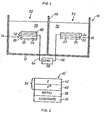
- Fig. 1 is a schematic representation of a liquid junction photoelectrochemical cell which incorporates both a photoanode and a photocathode in accordance with the invention;
- Fig. 2 is a section of a p-type photocathode in accordance with the invention;
- Fig. 3 is a section of a PIN type photocathode in accordance with the invention; and
- Fig. 4 is a section of an n-type photoanode in accordance with the invention.
- Referring to Fig. 1, a liquid junction
photoelectrochemical cell 10 for the photoelectrolysis of water is illustrated. Thecell 10 includes acontainer 12 with twophotoelectrodes membrane 18 and a photoanode 14 and aphotocathode 16. The photoelectrodes each have asubstrate deposition surface substrates - Conventional deposition techniques such as sputter deposition or evaporated deposition can be utilized to deposit a thin
reflective layer reflective layers - Next, a multilayer amorphous silicon
semiconductor alloy body reflective layers semiconductor alloy bodies - Specific embodiments of multilayer amorphous silicon alloy photoelectrodes are illustrated in Figs. 2, 3 and 4. Referring initially to Fig. 2, a p+ type photocathode 16' is illustrated which includes a stainless steel or
glass substrate 36 on which is deposited areflective layer 38, preferably of aluminum approximately 2000 angstroms thick. The multilayer amorphous silicon alloy body 34' is formed by first forming or otherwise depositing ap+ type layer 40 of a-Si:F:H or a-Si:Hx material doped with boron to a concentration of about 1023 atoms/cm3 on thereflective layer 38. Thep+ type layer 40 is a contact layer to which an electrical lead can be attached and has a preferred-thickness in the range of about 600 angstroms to 1500 angstroms. Finally, atop layer 42 of substantially intrinsic (I) a-Si:Hx or a-Si:F:H can be deposited to a thickness of about 5000 angstroms to 6000 angstroms. The top layer is very slightly doped p-type, such as with boron. The photocathode 16' can be formed with or without thetop layer 42. - Referring to Fig. 3, a
PIN type photocathode 16" is formed in accordance with the invention with a glass orstainless steel substrate 44, a molybdenumreflective layer 46 deposited on thesubstrate 44 to a thickness of about 2000 angstroms, a multilayer amorphous siliconsemiconductor alloy body 34" deposited on thereflective layer 46. The multilayer amorphous silicon semi-conductor alloy 34" is formed by first forming a p+ type a-Si:F:H or a-Si:Hxconductive layer 48 doped with boron to a concentration of about 1023 atoms/cm3. Thefirst layer 48 is preferably in the range of about 200 angstroms to 1500 angstroms thick. Alayer 50 of substantially intrinsic (I) (slightly n-doped) a-Si:F:H or a-Si:Hx semiconductor alloy of approximately 5000 to 6000 angstroms thick is formed on thelayer 48. Finally, a top layer 82 is formed of an n+ type a-Si:F:H or a-Si:Hx semiconductor alloy doped with phosphorus to a concentration of about 1027 atoms/cm3. - Referring to Fig. 4, an n-type photoanode 141 has a
substrate 54 which'is made from glass, stainless steel of other similar material and a reflectingmolybdenum layer 56 is formed thereon which is approximately 200 angstroms thick. An amorphous silicon alloy multilayer body 32' is formed by depositing an n+ type a-Si:F:H or a-Si:Hx semiconductor layer 58 doped with phosphorus to a concentration of about 1027 atoms/cm3. The-thickness of thefirst layer 58 is approximately 600 angstroms to 1500 angstroms. Next, alayer 60 of substantially intrinsic (I) (slightly n-doped) a-Si:F:H or a-Si:Hx semiconductor in the range of about 5000 angstroms to 6000 angstroms thick is deposited. Finally, atop oxide layer 62 is deposited or otherwise formed over the exposed surface of theintrinsic semiconductor layer 60 to primarily increase the conversion efficiency. - The
oxide layer 60 has a tunnelable thickness so that current will pass through theoxide layer 60 even though in bulk form the oxide layer can be an insulator. In order to assure the existence of the tunnel effect, theoxide layer 60 preferably is between about 10 angstroms and 40 angstroms in thickness depending upon the type of semiconductor material on which the oxide layer is deposited. The oxide layer can be either a native dielectric which, for example, is grown by oxidizing the surface of theintrinsic semiconductor layer 60 or can be a separately deposited dielectric. In the latter case, the oxide layer can be any of a number of different oxides including Nb205, Sb203, Si02, Ti02, Ta205 or any other suitable material which will operate to increase the conversion efficiency. Details of the construction and operation of oneoxide layer 62 are described in pending patent application Serial No. 353,767, entitled "Liquid Junction Photovoltaic Device With Tunnelable Interfacial Layer", filed March 1, 1982, which application is herein incorporated by reference. - In accordance with the invention, photoassisted electrolysis can occur utilizing both a photocathode such as the
photocathodes 16' and 16" described in conjunction with Figs. 2 or 3 and a photoanode such as the photoanode 14' described in connection with Fig. 4. Alternatively, only one photoelectrode along with a conventional metal counterelectrode can be utilized. - Returning to Fig. 1, the
photoelectrochemical device 10 illustrated has aphotoanode 14 and aphotocathode 16 constructed in the manner described in conjunction with Figs. 4 and 2. A pair of suitable electricallyconductive leads load 68. Asuitable electrolyte 70 is then placed in thecontainer 12 to cover thephotoelectrodes photons 72 impinge upon the electrodes, photoelectrolysis will occur according to the above described reactions. - Photoelectrodes have been utilized in photoelectrolysis as described in Example 1 and for the conversion of sunlight into electrical energy as described in Examples 2 through 4 hereafter. In photoelectrolysis, the operation can be assisted by replacing the
load 68 with a source of electrical power. - An a-Si:Hx (boron doped) ss/p+/p photocathode of the structure described in Fig. 2 was tested in a 1.0M KC1 electrolyte. The photocathode has a Voc vs. a SCE reference electrode of -.64V, a current of .34 MA/cm2 at a -1.20 volts at a light intensity of 45 mW/cm2. Hydrogen gas evolved from the electrode upon illumination of the electrode. A PIN type photocathode of the type described in Fig. 3 was tested under the same conditions and had a -.30 Voc, and 1.6mA/cm2 current at -1.20 volts.
- An n-type photoanode of the type described in Fig. 4 was tested in a half cell with an electrolyte of a 1M tetramethylammonium salt/ethenol containing ferrocenium ion redox couple. Conversion efficiencies of 2.4%, 1.1% and .45% were obtained at illuminations of 10mW/cm2, 45mW/cm2 and 100mW/cm2 respectively.
- A PIN-type photocathode of the type described in Fig. 3 was also tested for conversion of solar to electrical energy. The half cell electrolyte was a 30% aqueous acetonitrite containing .1 M KI 25mM methyviologen. Versus a SCE reference electrode, the Voc was .7V, and the Isc was 1.4 mA/cm2. Conversion efficiency was .22%.
- A p-type photocathode of the type described in fig. 2 was tested in the same cell as the PIN device. The p-type photocathode obtained efficiency of .05%, a Voc of .14V, and Isc of 1.1mA/cm2.
- Modifications and variations of the present invention are possible in light of the above teachings. For example, either or both of the
photoelectrodes
Claims (22)
Applications Claiming Priority (2)
| Application Number | Priority Date | Filing Date | Title |
|---|---|---|---|
| US46750183A | 1983-02-18 | 1983-02-18 | |
| US467501 | 1983-02-18 |
Publications (2)
| Publication Number | Publication Date |
|---|---|
| EP0117246A2 true EP0117246A2 (en) | 1984-08-29 |
| EP0117246A3 EP0117246A3 (en) | 1985-07-31 |
Family
ID=23855973
Family Applications (1)
| Application Number | Title | Priority Date | Filing Date |
|---|---|---|---|
| EP84850055A Withdrawn EP0117246A3 (en) | 1983-02-18 | 1984-02-16 | Liquid junction photoelectrodes using amorphous silicon-based thin film semiconductor |
Country Status (4)
| Country | Link |
|---|---|
| EP (1) | EP0117246A3 (en) |
| JP (1) | JPS59157976A (en) |
| AU (1) | AU2422684A (en) |
| CA (1) | CA1237510A (en) |
Cited By (6)
| Publication number | Priority date | Publication date | Assignee | Title |
|---|---|---|---|---|
| EP0820110A2 (en) * | 1996-07-19 | 1998-01-21 | Sony Corporation | Negative electrode material and non-aqueous liquid electrolyte secondary cell employing same |
| CN102713008A (en) * | 2009-07-09 | 2012-10-03 | 罗斯特里特实验室能源公司 | Tandem photoelectrochemical cell for water dissociation |
| WO2013152043A1 (en) * | 2012-04-02 | 2013-10-10 | California Institute Of Technology | Solar fuels generator |
| CN106684508A (en) * | 2016-11-28 | 2017-05-17 | 重庆大学 | Tiled type bipolar optical response photoelectric chemical battery, building roof domestic sewage treatment power generation system and working method |
| US10026560B2 (en) | 2012-01-13 | 2018-07-17 | The California Institute Of Technology | Solar fuels generator |
| CN114214639A (en) * | 2022-01-06 | 2022-03-22 | 承丰光能科技(广州)有限公司 | Photovoltaic and sunlight hydrolysis linkage coupling hydrogen production and oxygen production system |
Families Citing this family (4)
| Publication number | Priority date | Publication date | Assignee | Title |
|---|---|---|---|---|
| JPS61211965A (en) * | 1985-03-15 | 1986-09-20 | Matsushita Electric Ind Co Ltd | Photo-secondary cell |
| MX2011000963A (en) * | 2008-07-29 | 2011-05-23 | Yeda Res & Dev | System and method for hydrogen or syngas production. |
| DE102008051670A1 (en) * | 2008-10-15 | 2009-11-05 | H2 Solar Gmbh | Metallic or non-metallic silicides for photo-electrochemical decomposition of water and photovoltaic electricity generation, is illuminated, optionally in contact with water |
| JP6774165B2 (en) * | 2014-04-11 | 2020-10-21 | 株式会社豊田中央研究所 | Photochemical reaction device, electrode for oxidation reaction and electrode for reduction reaction used for it |
Citations (2)
| Publication number | Priority date | Publication date | Assignee | Title |
|---|---|---|---|---|
| US4215185A (en) * | 1979-03-26 | 1980-07-29 | Rca Corporation | Liquid junction schottky barrier solar cell |
| US4236984A (en) * | 1979-11-21 | 1980-12-02 | United Technologies Corporation | Hydrogen gas generation utilizing a bromide electrolyte, an amorphous silicon semiconductor and radiant energy |
Family Cites Families (3)
| Publication number | Priority date | Publication date | Assignee | Title |
|---|---|---|---|---|
| JPS54115091A (en) * | 1978-02-28 | 1979-09-07 | Katsumasa Haneda | Photoochemical diode |
| JPS55123176A (en) * | 1979-03-15 | 1980-09-22 | Sharp Corp | Thin film solar cell |
| JPH0614469B2 (en) * | 1982-01-08 | 1994-02-23 | 株式会社半導体エネルギー研究所 | Optical redox reactor |
-
1984
- 1984-02-06 AU AU24226/84A patent/AU2422684A/en not_active Abandoned
- 1984-02-16 JP JP59027964A patent/JPS59157976A/en active Pending
- 1984-02-16 EP EP84850055A patent/EP0117246A3/en not_active Withdrawn
- 1984-02-17 CA CA000447743A patent/CA1237510A/en not_active Expired
Patent Citations (2)
| Publication number | Priority date | Publication date | Assignee | Title |
|---|---|---|---|---|
| US4215185A (en) * | 1979-03-26 | 1980-07-29 | Rca Corporation | Liquid junction schottky barrier solar cell |
| US4236984A (en) * | 1979-11-21 | 1980-12-02 | United Technologies Corporation | Hydrogen gas generation utilizing a bromide electrolyte, an amorphous silicon semiconductor and radiant energy |
Non-Patent Citations (3)
| Title |
|---|
| APPLIED PHYSICS LETTERS, vol. 40, no. 3, 1st February 1982, pages 281-283, American Institute of Physics, New York, US; T. SKOTHEIM et al.: "A partially stabilized photoelectrochemical cell using hydrogenated amorphous silicon photoanodes coated with thin films of polypyrrole" * |
| CHEMICAL ABSTRACTS, vol. 99, no. 24, 12th December 1983, page 181, no. 198081n, Columbus, Ohio, US; & JP - A - 58 127 385 (SEMICONDUCTOR RESEARCH FOUNDATION) 29-07-1983 * |
| JOURNAL OF THE ELECTROCHEMICAL SOCIETY, vol. 129, no. 7, July 1982, pages 1644-1646, Manchester, New Hampshire, US; W.M. AYERS: "p-Type amorphous silicon/liquid junction solar cell" * |
Cited By (11)
| Publication number | Priority date | Publication date | Assignee | Title |
|---|---|---|---|---|
| EP0820110A2 (en) * | 1996-07-19 | 1998-01-21 | Sony Corporation | Negative electrode material and non-aqueous liquid electrolyte secondary cell employing same |
| EP0820110A3 (en) * | 1996-07-19 | 2000-03-01 | Sony Corporation | Negative electrode material and non-aqueous liquid electrolyte secondary cell employing same |
| CN102713008A (en) * | 2009-07-09 | 2012-10-03 | 罗斯特里特实验室能源公司 | Tandem photoelectrochemical cell for water dissociation |
| US10026560B2 (en) | 2012-01-13 | 2018-07-17 | The California Institute Of Technology | Solar fuels generator |
| US10242806B2 (en) | 2012-01-13 | 2019-03-26 | The California Institute Of Technology | Solar fuels generator |
| WO2013152043A1 (en) * | 2012-04-02 | 2013-10-10 | California Institute Of Technology | Solar fuels generator |
| US9476129B2 (en) | 2012-04-02 | 2016-10-25 | California Institute Of Technology | Solar fuels generator |
| US10344387B2 (en) | 2012-04-02 | 2019-07-09 | California Institute Of Technology | Solar fuels generator |
| CN106684508A (en) * | 2016-11-28 | 2017-05-17 | 重庆大学 | Tiled type bipolar optical response photoelectric chemical battery, building roof domestic sewage treatment power generation system and working method |
| CN114214639A (en) * | 2022-01-06 | 2022-03-22 | 承丰光能科技(广州)有限公司 | Photovoltaic and sunlight hydrolysis linkage coupling hydrogen production and oxygen production system |
| CN114214639B (en) * | 2022-01-06 | 2023-03-07 | 承丰光能科技(广州)有限公司 | Photovoltaic and sunlight hydrolysis linkage coupling hydrogen production and oxygen production system |
Also Published As
| Publication number | Publication date |
|---|---|
| CA1237510A (en) | 1988-05-31 |
| AU2422684A (en) | 1985-07-04 |
| JPS59157976A (en) | 1984-09-07 |
| EP0117246A3 (en) | 1985-07-31 |
Similar Documents
| Publication | Publication Date | Title |
|---|---|---|
| US4656103A (en) | Liquid junction photoelectrodes using amorphous silicon-based thin film semiconductor | |
| US4521499A (en) | Highly conductive photoelectrochemical electrodes and uses thereof | |
| US7052587B2 (en) | Photoelectrochemical device and electrode | |
| Tomkiewicz et al. | Photoelectrolysis of water with semiconductors | |
| US4592807A (en) | Methods of making highly conductive photoelectrochemical electrodes | |
| Aharon‐Shalom et al. | Efficient p‐InP (Rh‐H alloy) and p‐InP (Re‐H alloy) hydrogen evolving photocathodes | |
| Butler et al. | Principles of photoelectrochemical, solar energy conversion | |
| Young et al. | Photo-assisted water oxidation with cobalt-based catalyst formed from thin-film cobalt metal on silicon photoanodes | |
| Ghosh et al. | Photoelectrolysis of water in sunlight with sensitized semiconductor electrodes | |
| Aruchamy et al. | Semiconductor based photoelectrochemical cells for solar energy conversion—an overview | |
| US4790916A (en) | One-unit photo-activated electrolyzer | |
| US4501804A (en) | Photo-assisted electrolysis cell with p-silicon and n-silicon electrodes | |
| Anderson et al. | Becquerel effect solar cell | |
| EP0117246A2 (en) | Liquid junction photoelectrodes using amorphous silicon-based thin film semiconductor | |
| US4734168A (en) | Method of making n-silicon electrodes | |
| Mavroides | Electrode materials for the photoelectrolysis of water | |
| Wrighton | Thermodynamics and kinetics associated with semiconductor-based photoelectrochemical cells for the conversion of light to chemical energy | |
| US4439301A (en) | Photoelectrochemical cells including chalcogenophosphate photoelectrodes | |
| US4182796A (en) | Semiconductor liquid junction photocell using surface modified GaAs electrode | |
| Matsumura et al. | Photoelectrochemical hydrogen evolution using amorphous silicon electrodes having pin or pinpin junctions | |
| Ueda et al. | Efficient solar to chemical conversion with an n-type amorphous silicon/p-type crystalline silicon heterojunction electrode | |
| Rao | Recent trends in photoelectrochemical cells | |
| Licht et al. | The high aqueous solubility of K/sub 2/S and its effect on bulk and photoelectrochemical characteristics of Cd (SeTe)/S/sub X/= cells: II. Variation of sulfur/sulfide ratio | |
| Noufi et al. | Electrochemical solar cells: principles and recent results | |
| Maugh | Catalysis in Solar Energy: Photoelectrochemical cells approach the efficiency of photovoltaics, but durability and cost are still major hurdles |
Legal Events
| Date | Code | Title | Description |
|---|---|---|---|
| PUAI | Public reference made under article 153(3) epc to a published international application that has entered the european phase |
Free format text: ORIGINAL CODE: 0009012 |
|
| AK | Designated contracting states |
Designated state(s): AT BE CH DE FR GB IT LI LU NL SE |
|
| 17P | Request for examination filed |
Effective date: 19850211 |
|
| PUAL | Search report despatched |
Free format text: ORIGINAL CODE: 0009013 |
|
| AK | Designated contracting states |
Designated state(s): AT BE CH DE FR GB IT LI LU NL SE |
|
| 17Q | First examination report despatched |
Effective date: 19870921 |
|
| STAA | Information on the status of an ep patent application or granted ep patent |
Free format text: STATUS: THE APPLICATION IS DEEMED TO BE WITHDRAWN |
|
| 18D | Application deemed to be withdrawn |
Effective date: 19880406 |
|
| PGFP | Annual fee paid to national office [announced via postgrant information from national office to epo] |
Ref country code: DK Payment date: 20001215 Year of fee payment: 6 |
|
| RIN1 | Information on inventor provided before grant (corrected) |
Inventor name: PINSKY, NAUM Inventor name: LIANG, GAO Inventor name: SAPRU, KRISHNA Inventor name: REICHMAN, BENJAMIN |