EP0111827B1 - Multichannel apparatus measuring varying weak magnetic fields, and method of manufacturing the same - Google Patents
Multichannel apparatus measuring varying weak magnetic fields, and method of manufacturing the same Download PDFInfo
- Publication number
- EP0111827B1 EP0111827B1 EP83112270A EP83112270A EP0111827B1 EP 0111827 B1 EP0111827 B1 EP 0111827B1 EP 83112270 A EP83112270 A EP 83112270A EP 83112270 A EP83112270 A EP 83112270A EP 0111827 B1 EP0111827 B1 EP 0111827B1
- Authority
- EP
- European Patent Office
- Prior art keywords
- gradiometer
- coils
- measuring device
- carrier
- chip
- Prior art date
- Legal status (The legal status is an assumption and is not a legal conclusion. Google has not performed a legal analysis and makes no representation as to the accuracy of the status listed.)
- Expired
Links
Images


Classifications
-
- G—PHYSICS
- G01—MEASURING; TESTING
- G01R—MEASURING ELECTRIC VARIABLES; MEASURING MAGNETIC VARIABLES
- G01R33/00—Arrangements or instruments for measuring magnetic variables
- G01R33/02—Measuring direction or magnitude of magnetic fields or magnetic flux
- G01R33/035—Measuring direction or magnitude of magnetic fields or magnetic flux using superconductive devices
- G01R33/0354—SQUIDS
- G01R33/0356—SQUIDS with flux feedback
-
- G—PHYSICS
- G01—MEASURING; TESTING
- G01R—MEASURING ELECTRIC VARIABLES; MEASURING MAGNETIC VARIABLES
- G01R33/00—Arrangements or instruments for measuring magnetic variables
- G01R33/0017—Means for compensating offset magnetic fields or the magnetic flux to be measured; Means for generating calibration magnetic fields
-
- G—PHYSICS
- G01—MEASURING; TESTING
- G01R—MEASURING ELECTRIC VARIABLES; MEASURING MAGNETIC VARIABLES
- G01R33/00—Arrangements or instruments for measuring magnetic variables
- G01R33/02—Measuring direction or magnitude of magnetic fields or magnetic flux
- G01R33/035—Measuring direction or magnitude of magnetic fields or magnetic flux using superconductive devices
- G01R33/0354—SQUIDS
- G01R33/0358—SQUIDS coupling the flux to the SQUID
Definitions
- the invention relates to a device for multichannel measurement of weak, changing magnetic fields in a field strength range below 10- 10 T, in particular below 10- 12 T, which in each channel a superconducting quantum interference element (SQUID), by superconducting coils formed gradiometer and superconducting links between the quantum interference element and the gradiometer with a coupling transformer and connecting conductor, and which further includes electronic devices for evaluating, processing and displaying the information obtained on the quantum interference elements.
- the invention further relates to a method for producing this measuring device.
- SQUIDS superconducting Quantum Interference Devices
- Magnetic heart and brain waves occurring with field strengths in the order of magnitude of 50 pT or 0.1 pT ("Biomagnetism - Proceedings Third International Workshop on Biomagnetism, Berlin 1980 ", Berlin / New York 1981, pages 3 to 31).
- the magnetic field to be examined is inductively coupled into the circuit formed by a radio frequency (RF) -SQUID with a Josephson contact via a coil arrangement made of superconducting wire.
- Gradiometers of first or higher order are formed by combining a sensor coil with one or more compensation coils. With such gradiometers, the three components of a magnetic field which is homogeneous in the coil area or also its portion with a homogeneous gradient can be largely suppressed with a corresponding manual adjustment and the biomagnetic near field, which is still very inhomogeneous in the gradiometer area, can be selectively detected.
- the RF-SQUID is also inductively coupled to a resonant circuit whose high-frequency voltage is modulated in phase or amplitude by the input signal.
- the operating point of the RF-SQUID is recorded by negative feedback via an additional compensation coil and the compensation current is used as a signal to be evaluated electronically.
- the RF-SQUIDs used in these systems have a characteristic noise signal (see, for example, "SQUID-Superconducting Quantum Interference Devices and their Applications", Berlin / New York 1977, pages 395 to 431).
- a signal mean value formation must be carried out at the individual measuring points by a large number of individual measurements.
- measurements must also be taken in succession at different locations in the area to be examined. The difficulty with these measurement methods is then that the coherence of the field data is no longer ensured over the measurement time required for this and that clinically unreasonable measurement times also result.
- a measuring device with three RF-SQUIDs and only one resonance circuit on a common carrier structure is already known from the publication "Cryogenics", December 1981, pages 707 to 710, which supports the preamble of claim 1.
- it is a technical problem with this device that all signal channels are combined in a high-frequency channel with mutual interference and that the individual SQUID elements must be matched to one another with regard to their critical current.
- the number of maximum controllable elements in practice is therefore considered to be about 10.
- DC-SQUIDs In addition to the mentioned RF-SQUIDs, each with a Josephson contact, direct current (DC) -S (2U1Ds) are known, which comprise two Josephson contacts. These DC-SQUIDs can be designed in such a way that they have an extremely small noise signal ( "IEEE Transactions on Magnetics", Vol.MAG-17, No.1, January 1981, pages 395 to 399)
- DC-SQUIDs can be designed in such a way that they have an extremely small noise signal ( "IEEE Transactions on Magnetics", Vol.MAG-17, No.1, January 1981, pages 395 to 399)
- the use of a modular system with 5 SQUIDs of this type for measuring biomagnetic fields is contemplated a mutual RF interference is not to be feared, however, the mentioned tuning problem is also present here.
- the object of the present invention is, using DC-SQUIDs, to improve the proposed device for multichannel measurement of weak, changing magnetic fields in such a way that it can be used to determine the spatial field distribution of biomagnetic fields during reasonable measuring times Coherence of the field data is guaranteed.
- This object is achieved in that a common rigid support structure for DC-SQUIDs and their associated, planar-shaped gradiometer coils and the superconducting connecting elements is provided, the gradiometer coils and the connecting elements being arranged as thin-film structures in one or more planes are.
- FIG. 1 shows a circuit diagram of a measuring device according to the invention.
- FIG. 2 schematically shows a carrier structure of this device with SQUIDs and gradiometers, while FIGS. 3 and 4 illustrate a carrier for a corresponding SQUID chip.
- FIG. 5 shows a further structure of a device according to the invention, of which a connection of its conductor tracks is shown in detail in FIGS. 6 and 7.
- each channel contains a superconducting gradiometer 2 and a DC-SQUID 4 equipped with two Josephson contacts 3, a superconducting link 5 for connecting the gradiometer to the SQUID 4, also a preamplifier 6, which is also cooled, for example, and a so-called "lock-in" - amplifier 7.
- the N raw signals extracted from the lock-in amplifiers 7 are then fed to a common electronic data processing and control system 8a for further processing and an output unit 8b for display.
- a feedback in the channels to the respective SQUIDs with the signals taken from the look-in amplifiers 7 is indicated by dotted lines 9.
- the signal transmission directions are illustrated in the figure by arrows on the corresponding lines.
- the gradiometers 2, the SQUIDs 4 and the connecting links 5 required between them should be arranged on a common, rigid support structure.
- This support structure is indicated in the figure by a dashed line labeled 10a.
- the SQUIDs 4 with their associated thin-film transformers are located on a carrier plate (chip) 10b which is fixedly arranged on the carrier structure 10a.
- the signals generated at the individual gradiometer coils 2 can advantageously be combined in a predetermined manner in the measuring device according to the invention. Accordingly, for example in the exemplary embodiment indicated in FIG. 1, the signals from two or three of the gradiometer coils 2 can be combined.
- the signals are summarized preferably in the area of the electronics 8a common to all coils by means of corresponding logic circuits.
- each gradiometer coil in the case of a round shape, its diameter, are advantageously adapted to the distance to the closest magnetic field source to be detected with regard to optimal spatial resolution. So you choose e.g. for magnetoenzophalographic examinations generally a diameter of about 2 cm, which is optimal for measurements of sources in the cerebral cortex.
- the aforementioned combination of the signals of individual gradiometer coils then sets coil ratios that largely correspond to effective coil dimensions that are optimal for these larger distances between the magnetic field source and the coil.
- Gradiometers of the first order place lower requirements with regard to shielding, two embodiments being indicated in FIGS. 2 and 5. While the gradiometer row indicated in FIG. 2 is designed planar, the gradiometer row shown in FIG. 5 is an arrangement in two planes.
- a planar gradiometer row also called a gradiometer field (array) is applied to a flat carrier structure 11, for example a quartz or silicon plate of approximately 10 mm thick, 12 cm wide b and 30 cm long 1.
- This gradiometer row, designated 12 is formed by a row 13 of detection coils 14, by a row 15 with a corresponding number of compensation coils 16 and by corresponding connecting lines 17.
- Each of the rows 13 and 15 consists, for example, of 4 by 5 individual superconducting flat coils, each with one turn, the diameter D of which is approximately in the order of the distance from the object to be examined and is thus, for example, a few centimeters.
- the detection coils 14 can also be provided.
- the detection coils can be enclosed by a ring made up of the individual compensation coils.
- the compensation flat coil field 15 can advantageously also be replaced by a smaller field of coils with a correspondingly increased number of turns. This can be achieved, for example, by means of a lithography process with the aid of an insulating intermediate layer.
- the carrier structure 11 there is also a small plate (chip) 19 with a number of DG-SQUIDs corresponding to the number of gradiometers, including superconducting coupling transformers and modulation coils with connections. Silicon is generally chosen as the chip material.
- the coupling transformers can be designed in a known manner as flat coils (cf. "IEEE Trans.Magn.”, Vol. MAG-17, No.1, January 1981, pages 400 to 403).
- the respective connecting lines 17 for supplying the field signals registered in the gradiometer coils are connected superconductingly to these coupling transformers.
- the signals picked up at the individual SQUIDs are then fed via a normally conducting input / output lines 21, which are connected to the DC-SQUID chip 19 at corresponding connection points 22, to a multiple contact strip 23, to which the amplifiers of the respective channels are then connected .
- a special chip carrier can advantageously be used in the case of a solder connection technique at the connections 20 in order to reduce or avoid different thermal expansions.
- a relatively simple chip exchange is also made possible.
- a Exemplary embodiment for a corresponding chip carrier can be seen from the top view or the longitudinal section of FIGS. 3 and 4.
- the chip carrier denoted by 25 advantageously consists of the same material as the chip 26 arranged on it and carrying the SOUIDs and their thin-film transformers, ie, for example, made of Si, while the gradiometer-carrying plate 27 consists of quartz, for example.
- the chip 26 is fastened to the underside of the chip carrier 25 by soldering 33 of the conductor tracks.
- a corresponding recess 34 is therefore provided in the quartz carrier plate 27.
- the chip carrier 25 can protrude a bit beyond the carrier plate 27. It is thus possible to engage a connector 35 on this side of the carrier 25 for connecting the SQUIDs to subsequent amplifiers directly on corresponding normally conductive conductor tracks.
- planar gradiometer row 12 with the detection coils 14 and the compensation coils 16 is first realized in a known planar lithography step in the form of superconducting thin-film coil fields, for example made of lead, on this carrier plate 11.
- the connecting lines 17 of the individual coils with one another and their crossover points 18 can also be produced as a thin-film structure.
- the DC-SQUID series is made, for example, of niobium according to those in DE-A-31 28 982, 31 29 000, 32 20 211 and 32 20 251, published on February 10, 1983, 17.2.1983, and December 1, 1983, respectively and 1.12.1983.
- the superconducting coupling transformers and modulation coils with connections e.g. made of lead in a technology known from the production of integrated circuits on the silicon chip 19 in the form of a multilayer thin-film structure.
- the gradiometer coils are adjusted once.
- a laser beam can be used for this purpose, with which the width of the individual coil turns can be reduced.
- a planar structure can advantageously be provided in several planes.
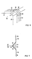
- An embodiment of a corresponding first order gradiometer structure is shown schematically in the oblique view shown in FIG. In the selected view, parts shaded by the support structure are partially indicated by dashed lines.
- the carrier structure 37 is essentially composed of two cuboidal parts 38 and 39 which are rigidly joined to one another for receiving gradiometer coils 40 and 41 or a DC-SQUID chip 42. Only some of the gradiometer coils with their corresponding connecting lines are illustrated in the figure.
- the further columnar support structure part 39 for example also a quartz prism, rigidly connected.
- This columnar prism has a cross section adapted to the size of the DC SQUID chip 42.
- This chip is arranged, for example, on the side 51 of the columnar quartz prism 39 facing away from the flat side 44.
- conductor tracks 52 corresponding to the conductor tracks 45 are first provided from the individual detection coils 40 to the edge 47 of the flat side 43.
- the chip 42 can also be fastened on the side surface 55.
- interconnect connections at the edge 56 can advantageously be saved.
- the arrangement of the detection coils 40 and the compensation coils 41 in two parallel planes of a support structure, e.g. 5 leads to the fact that there are orthogonal planes which can advantageously be used to enable additional detection loops, for example in thin film technology, to be attached in these planes, with which the three vector components of the magnetic field can be determined for the purpose of adaptive filtering (cf. "Rev.Sci.lnstrum.”, Vol. 53, No. 12, 1982, pages 1815 to 1845, in particular page 1836).
- connection of the conductor tracks 52 to the conductor tracks 53 at the edge 47 is advantageously carried out in accordance with one in DE-A-32 46 661, published on June 20, 1984, with the title: "Method for producing electrical lines leading around an outer edge", proposed method and is indicated in the oblique view of Figure 6 for two interconnect connections. Parts corresponding to FIG. 5 are provided with the same reference symbols.
- a groove 58 is first vertically worked into the edge 47 between the two flat sides 43 and 49 at each predetermined connection point, before a thin film of the material of the conductor tracks is applied to the flat sides, including the walls of the grooves.
- the conductor tracks are formed by removing the unnecessary parts of the applied films.
- edge 47 is slightly chamfered in order to obtain sharper boundaries between coated and non-coated parts.
- soldering can additionally be carried out on the base of the groove between the respective transition points to the parts deposited in the grooves 58. Corresponding solder joints are designated 59 in the figure. Superconducting lead-indium solder is particularly suitable for this.
- connections of the conductor tracks 50 to the conductor tracks 45 and 46 and the connections at the edge 56 can also be established.
- FIG. 7 schematically illustrates the transition of the conductor tracks from the prism 38 carrying the gradiometer coils 40 and 41 to the prism 39 carrying the DC-SQUID chip 42 as a section through the corresponding part of the structure according to FIG.
- these are first provided with connecting pieces in grooves 62 and 63 on the respective edges 48 and 61, respectively, in accordance with the method indicated in FIG.
- the sides 49 and 55 of the two prisms 38 and 39 are then joined together in such a way that the conductor parts abut one another in these grooves 62 and 63.
- a soldering 64 is finally made e.g. with a lead alloy after the film coverings in the grooves are galvanically reinforced.
- a graphic representation of measures for shielding the DC-SQUIDs against magnetic interference fields has been omitted for reasons of clarity.
- Appropriate measures are generally known.
- the SQUIDs on the chip can be individually surrounded by closed superconducting ring structures. Coating the back of the chip with superconducting material is also possible. If a special chip carrier is used, this can also be provided with a corresponding layer on its back. In this case, the chip and its chip carrier can also be surrounded by a superconducting sleeve which is closed except for an opening on the leads.
Description
Die Erfindung bezieht sich auf eine Vorrichtung zur mehrkanaligen Messung schwacher, sich ändernder Magnetfelder in einem Feldstärkebereich unter 10-10 T, insbesondere unter 10-12 T, welche in jedem Kanal ein supraleitendes Quanten-Interferenz- Element (SQUID), ein durch supraleitende Spulen gebildetes Gradiometer sowie supraleitende Verknüpfungsglieder zwischen dem Quanten-Interferenz- Element und dem Gradiometer mit einem Koppeltransformator und Verbindungsleiter enthält, und welche ferner elektronische Einrichtungen zur Auswertung, Verarbeitung und Darstellung der an den Quanten-Interferenz-Elementen gewonnenen Informationen umfaßt. Die Erfindung betrifft ferner ein Verfahren zur Herstellung dieser Meßvorrichtung.The invention relates to a device for multichannel measurement of weak, changing magnetic fields in a field strength range below 10- 10 T, in particular below 10- 12 T, which in each channel a superconducting quantum interference element (SQUID), by superconducting coils formed gradiometer and superconducting links between the quantum interference element and the gradiometer with a coupling transformer and connecting conductor, and which further includes electronic devices for evaluating, processing and displaying the information obtained on the quantum interference elements. The invention further relates to a method for producing this measuring device.
Die Verwendung von supraleitenden Quanten-Interferenz-Elementen, die allgemein als "SQUIDS" (Abkürzung von "Superconducting Quantum Interference Devices") bezeichnet werden, zur Messung sehr schwacher magnetischer Felder ist allgemein bekannt ("J.Phy.E:Sci. Instrum.", Vol. 13, 1980, Seiten 801 bis 813; "IEEE Transactions on Electron Devices", Vol. ED-27, No.10, Oktober 1980, Seiten 1896 bis 1908). Als ein bevorzugtes Anwendungsgebiet für diese Elemente wird deshalb auch die medizinische Technik, insbesondere die Magnetokardiographie und Magnetoenzephalographie angesehen, wobei magnetische Herz- und Gehirnwellen mit Feldstärken in der Größenordnung von 50 pT bzw. 0,1 pT auftreten ("Biomagnetism - Proceedings Third International Workshop on Biomagnetism, Berlin 1980", Berlin/New York 1981, Seiten 3 bis 31).The use of superconducting quantum interference elements, commonly referred to as "SQUIDS" (abbreviation of "Superconducting Quantum Interference Devices"), for measuring very weak magnetic fields is generally known ("J.Phy.E: Sci. Instrum. ", Vol. 13, 1980, pages 801 to 813;" IEEE Transactions on Electron Devices ", Vol. ED-27, No.10, October 1980, pages 1896 to 1908). Medical technology, in particular magnetocardiography and magnetoencephalography, is therefore also regarded as a preferred field of application for these elements, magnetic heart and brain waves occurring with field strengths in the order of magnitude of 50 pT or 0.1 pT ("Biomagnetism - Proceedings Third International Workshop on Biomagnetism, Berlin 1980 ", Berlin / New York 1981, pages 3 to 31).
Eine Vorrichtung zur Messung derartiger biomagnetischer Felder enthält im wesentlichen folgende Komponenten:
- 1. Ein SQUID, den eigentlichen Feld-Sensor,
- 2. einen Flußtransformator, eine Spulenanordnung zur Einkopplung des zu untersuchenden Feldes,
- 3. elektronische Geräte zur Signalerfassung und -verarbeitung,
- 4. Abschirmungen für das magnetische Erdfeld und externe Störfelder und
- 5. ein Kryosystem für den Tieftemperaturbereich der Supraleitung. Entsprechende Vorrichtungen sind bekannt (Firma S.H.E. Corporation, San Diego, USA/S.H.E. GmbH, D-5100 Aachen).
- 1. A SQUID, the actual field sensor,
- 2. a flux transformer, a coil arrangement for coupling the field to be examined,
- 3. electronic devices for signal acquisition and processing,
- 4. Shields for the magnetic earth field and external interference fields and
- 5. a cryosystem for the low temperature range of superconductivity. Corresponding devices are known (SHE Corporation, San Diego, USA / SHE GmbH, D-5100 Aachen).
Bei entsprechenden einkanalig ausgebildeten Vorrichtungen wird das zu untersuchende Magnetfeld über eine Spulenanordnung aus supraleitendem Draht in den von einem Radiofrequenz (RF)-SQUID gebildeten Kreis mit einem Josephson-Kontakt induktiv eingekoppelt. Dabei sind durch Kombination einer Sensorspule mit einer oder mehreren Kompensationsspulen Gradiometer erster bzw. höherer Ordnung ausgebildet. Mit solchen Gradiometern können bei entsprechendem manuellen Abgleich die drei Komponenten eines im Spulenbereich homogenen Magnetfeldes bzw. auch dessen Anteil mit homogenem Gradienten weitgehend unterdrückt und das im Gradiometerbereich noch stark inhomogene biomagnetische Nahfeld selektiv erfaßt werden. Das RF-SQUID ist außerdem mit einem Resonanzschwingkreis induktiv gekoppelt, dessen hochfrequente Spannung in Phase oder Amplitude durch das Eingangssignal moduliert wird. Im allgemeinen wird durch negative Rückkopplung über eine zusätzliche Kompensationsspule der Arbeitspunkt des RF-SQUID festgehalten und der Kompensationsstrom als elektronisch auszuwertendes Signal verwendet.In corresponding single-channel devices, the magnetic field to be examined is inductively coupled into the circuit formed by a radio frequency (RF) -SQUID with a Josephson contact via a coil arrangement made of superconducting wire. Gradiometers of first or higher order are formed by combining a sensor coil with one or more compensation coils. With such gradiometers, the three components of a magnetic field which is homogeneous in the coil area or also its portion with a homogeneous gradient can be largely suppressed with a corresponding manual adjustment and the biomagnetic near field, which is still very inhomogeneous in the gradiometer area, can be selectively detected. The RF-SQUID is also inductively coupled to a resonant circuit whose high-frequency voltage is modulated in phase or amplitude by the input signal. In general, the operating point of the RF-SQUID is recorded by negative feedback via an additional compensation coil and the compensation current is used as a signal to be evaluated electronically.
Die in diesen Anlagen eingesetzten RF-SQUIDs weisen ein charakteristisches Rausch-Signal auf (vgl.z.B. "SQUID-Superconducting Quantum Inter- ferenz Devices and their Applications", Berlin/ New York 1977, Seiten 395 bis 431). Zur Ermittlung der genannten, extrem schwachen Magnetfelder muß deshalb an den einzelnen Meßpunkten eine Signalmittelwertbildung durch eine Vielzahl von Einzelmessungen vorgenommen werden. Um eine räumliche Feldverteilung zu erhalten, muß außerdem zeitlich nacheinander an verschiedenen Orten des zu untersuchenden Bereiches gemessen werden. Bei diesen Meßverfahren besteht dann die Schwierigkeit, daß über die hierfür erforderliche Meßzeit die Kohärenz der Felddaten nicht mehr gegeben ist und sich außerdem klinisch unzumutbare Meßzeiten ergeben.The RF-SQUIDs used in these systems have a characteristic noise signal (see, for example, "SQUID-Superconducting Quantum Interference Devices and their Applications", Berlin / New York 1977, pages 395 to 431). To determine the extremely weak magnetic fields mentioned, a signal mean value formation must be carried out at the individual measuring points by a large number of individual measurements. In order to obtain a spatial field distribution, measurements must also be taken in succession at different locations in the area to be examined. The difficulty with these measurement methods is then that the coherence of the field data is no longer ensured over the measurement time required for this and that clinically unreasonable measurement times also result.
Es ist deshalb vorgeschlagen worden, statt der bekannten einkanaligen Messung eine mehrkanalige vorzunehmen, wobei jeder Kanal neben einem RF-SQUID ein abstimmbares supraleitendes Gradiometer und Verknüpfungsglieder zwischen dem SQUID und dem Gradiometer mit einem Koppeltransformator und Verbindungsleitern aufweist. Bei einer entsprechenden Vorrichtung ergibt sich jedoch ein erheblicher, zeitraubender Aufwand hinsichtlich der Abstimmung der einzelnen Kanäle aufeinander. Gemäß der bekannten Vorrichtung sind nämlich das Gradiometer einerseits und das SQUID mit seinem Koppeltransformator andererseits jeweils auf einer eigenen Trägerstruktur angeordnet und werden über lösbare Verbindungsleiter aneinander angeschlossen. Mit einer derartigen Verbindungstechnik läßt sich jedoch eine konstante Abstimmung des jeweiligen Flußtransformators nicht von vornherein gewährleisten. Vielmehr ist vor jeder Messung ein Abgleich aller Kanäle erforderlich, die sich auch untereinander beeinflussen. Außerdem ist bei einer solchen Anordnung eine gegenseitige Störung der RF-Kreise unvermeidlich. Wenn man auf die Gradiometer verzichtete, kann zwar eine RF-Abschirmung erreicht werden (vgl. z.B. "Physica", Band 107B, 1981, Seiten 29 und 30). Aber selbst wenn sich eine RF-Entkopplung auf anderem Wege lösen ließe, bleibt das erwähnte Abstimmproblem.It has therefore been proposed to carry out a multi-channel measurement instead of the known single-channel measurement, each channel having an RF-SQUID, a tunable superconducting gradiometer and links between the SQUID and the gradiometer with a coupling transformer and connecting conductors. With a corresponding device, however, there is a considerable, time-consuming effort with regard to the coordination of the individual channels with one another. According to the known device, the gradiometer on the one hand and the SQUID with its coupling transformer on the other hand are each arranged on their own support structure and are connected to one another via detachable connecting conductors. With such a connection technology, however, constant tuning of the respective flux transformer cannot be guaranteed from the outset. Rather, a comparison of all channels that influence each other is required before each measurement. In addition, mutual interference between the RF circuits is inevitable with such an arrangement. If the gradiometer is dispensed with, RF shielding can be achieved (see, for example, "Physica", volume 107B, 1981,
Eine Meßvorrichtung mit drei RF-SQUIDs und nur einem Resonanzkreis auf einer gemeinsamen Trägerstuktur ist zwar bereits aus der Veröffentlichung "Cryogenics", Dezember 1981, Seiten 707 bis 710 bekannt, die den Oberbegriff von Anspruch 1 belegt. Jedoch ist es bei dieser Vorrichtung ein technisches Problem, daß alle Signalkanäle in einem Hochfrequenzkanal mit gegenseitiger Störmöglichkeit zusammengefaßt werden und daß die einzelnen SQUID-Elemente hinsichtlich ihres kritischen Stromes aufeinander abgestimmt sein müssen. Die Zahl der in der Praxis maximal beherrschbaren Elemente wird deshalb bei etwa 10 angesehen.A measuring device with three RF-SQUIDs and only one resonance circuit on a common carrier structure is already known from the publication "Cryogenics", December 1981, pages 707 to 710, which supports the preamble of
Neben den genannten RF-SQUIDs mit jeweils einem Josephson-Kontakt sind auch Gleichstrom (DC)-S(2U1Ds bekannt, welche zwei Josephson-Kontakte umfassen. Deise DC-SQUIDs lassen sich so gestalten, daß sie ein äußerst kleines Rausch-Signal aufweisen ("IEEE Transactions on Magnetics", Vol.MAG-17, No.1, Januar 1981, Seiten 395 bis 399). An einen Einsatz eines modular aufgebauten Sysems mit 5 SQUlDs dieses Typs zur Messung biomagnetischer felder ist gedacht. Zwar ist bei dieser Vorrichtung eine gegenseitige RF-Störung nicht zu befürchten, jedoch ist auch hier das erwähnte Abstimmproblem gegeben.In addition to the mentioned RF-SQUIDs, each with a Josephson contact, direct current (DC) -S (2U1Ds) are known, which comprise two Josephson contacts. These DC-SQUIDs can be designed in such a way that they have an extremely small noise signal ( "IEEE Transactions on Magnetics", Vol.MAG-17, No.1, January 1981, pages 395 to 399) The use of a modular system with 5 SQUIDs of this type for measuring biomagnetic fields is contemplated a mutual RF interference is not to be feared, however, the mentioned tuning problem is also present here.
Aufgabe der vorliegenden Erfindung ist es, unter Verwendung von DC-SQUIDs die vorgeschlagene, eingangs genannte Vorrichtung zur mehrkanaligen Messung schwacher, sich ändernder Magnetfelder dahingehend zu verbessern, daß mit ihr die räumliche Feldverteilung von biomagnetischen Feldern während zumutbarer Meßzeiten ermittelt werden kann, wobei eine weitgehende Kohärenz der felddaten gewährleistet ist.The object of the present invention is, using DC-SQUIDs, to improve the proposed device for multichannel measurement of weak, changing magnetic fields in such a way that it can be used to determine the spatial field distribution of biomagnetic fields during reasonable measuring times Coherence of the field data is guaranteed.
Diese Aufgabe wird erfindungsgemäß dadurch gelöst, daß eine gemeinsame starre Trägerstruktur für DC-SQUIDs und die ihnen zugeordneten, planar gestalteten, Gradiometer- Spulen sowie die supraleitenden Verknüpfungsgliedern vorgesehen ist, wobei die Gradiometer-Spulen und die Verknüpfungsglieder als Dünnfilmstrukturen in einer oder mehreren Ebenen angeordnet sind.This object is achieved in that a common rigid support structure for DC-SQUIDs and their associated, planar-shaped gradiometer coils and the superconducting connecting elements is provided, the gradiometer coils and the connecting elements being arranged as thin-film structures in one or more planes are.
Bei dieser Ausgestaltung der Meßvorrichtung ist somit eine parallele, d.h. gleichzeitige Registrierung der Feldwerte von verschiedenen Oten aus mit Hilfe einer Reihe von supraleitenden Gradiometer-Spulen ermöglicht, die mit einer entsprechenden Reihe von DC-SQUIDs zu einem starren System verknüpft sind. Hiermit läßt sich vorteilhaft die Meßzeit entsprechend der Anzahl der Kanäle reduzieren. Außerdem ist bei dem erfindungsgemäßen Aufbau unter Verwendung von Dünnfilmstrukturen nur ein einmaliger Abgleich erforderlich.With this configuration of the measuring device, a parallel, i.e. Simultaneous registration of the field values from different locations is made possible by means of a series of superconducting gradiometer coils, which are linked to a corresponding series of DC-SQUIDs to form a rigid system. This advantageously reduces the measuring time according to the number of channels. In addition, only a single adjustment is required in the construction according to the invention using thin film structures.
Vorteilhafte Ausgestaltungen der Meßvorrichtung nach der Erfindung bzw. ein Verfahren zur Herstellung einer solchen Meßvorrichtung gehen aus den Unteransprüchen hervor.Advantageous refinements of the measuring device according to the invention and a method for producing such a measuring device are evident from the subclaims.
Zur weiteren Erläuterung der Erfindung und deren in den Unteransprüchen gekennzeichneten Weiterbildungen wird auf die Zeichnung Bezug genommen, in deren Figur 1 ein Schaltungsschema einer Meßvorrichtung nach der Erfindung angedeutet ist. Die figur 2 zeigt schematisch eine Trägerstruktur dieser Vorrichtung mit SQUlDs und Gradiometern, während in den Figuren 3 und 4 ein Träger für einen entsprechenden SQUID-Chip veranschaulicht ist. In Figur 5 ist ein weiterer Aufbau einer erfindungsgemäßen Vorrichtung dargestellt, von der in den Figuren 6 und 7 jeweils als Detail eine Verbindung ihrer Leiterbahnen gezeigt ist.To further explain the invention and its developments characterized in the subclaims, reference is made to the drawing, in which FIG. 1 shows a circuit diagram of a measuring device according to the invention. FIG. 2 schematically shows a carrier structure of this device with SQUIDs and gradiometers, while FIGS. 3 and 4 illustrate a carrier for a corresponding SQUID chip. FIG. 5 shows a further structure of a device according to the invention, of which a connection of its conductor tracks is shown in detail in FIGS. 6 and 7.
Gemäß dem in Figur 1 angedeuteten Schaltungsschema der Meßvorrichtung nach der Erfindung ist eine vorbestimmte Anzahl N paralleler Meßkanäle vorgesehen. Jeder Kanal enthält dabei ein supraleitendes Gradiometer 2 und ein mit zwei Josephson-Kontakten 3 ausgestattetes DC-SQUID 4, ein supraleitendes Verknüpfungsglied 5 zur Verbindung des Gradiometers mit dem SQUID 4, ferner einen beispielsweise ebenfalls gekühlten Vorverstärker 6 sowie einen sogenannten "Lock-in"- Verstärker 7.According to the circuit diagram of the measuring device according to the invention indicated in FIG. 1, a predetermined number N of parallel measuring channels is provided. Each channel contains a superconducting gradiometer 2 and a DC-SQUID 4 equipped with two Josephson contacts 3, a
Die aus den Lock-in-Verstärkern 7 entnommenen N Rohsignale werden dann einem gemeinsamen elektronischen Datenverarbeitungs- und Steuerungssystem 8a zur Weiterverarbeitung und einer Ausgabeeinheit 8b zur Darstellung zugeführt. Eine Rückkopplung in den Kanälen an die jeweiligen SQUIDs mit den den Look-in-Verstärkern 7 entnommenen Signalen ist durch gepunktete Linien 9 angedeutet. Die Signalübertragungsrichtungen sind in der Figur durch Pfeile an den den entsprechenden Linien veranschaulicht.The N raw signals extracted from the lock-in
Wie in der Figur ferner durch gestrichelte Linien dargestellt ist, sollen gemäß der Erfindung die Gradiometer 2, die SQUIDs 4 sowie die zwischen ihnen erforderlichen Verbindungsglieder 5 auf einer gemeinsamen, starren Trägerstruktur angeordnet sein. Diese Trägerstruktur ist in der Figur durch eine mit 10a bezeichnete, gestrichelte Linie angedeutet. In entsprechender Weise ist ferner veranschaulicht, daß sich die SQUIDs 4 mit ihren zugeordneten Dünnfilmtransformatoren auf einem Trägerplättchen (Chip) 10b befinden, das fest auf der Trägerstruktur 10a angeordnet ist.As further shown in the figure by dashed lines, according to the invention the gradiometers 2, the SQUIDs 4 and the connecting
Bekanntlich ergeben sich für eine vorbestimmte Entfernung zwischen einer Gradiometer-Spule 2 und einer von ihr zu detektierenden Magnetfeldquelle z.B. im Herzen bestimmte optimale Abmessungen der Gradiometer-Spulen hinsichtlich der Empfindlichkeit ("Journal of Magnetism and Magnetic Materials", Band 22, 1982, Nr. 2, Seiten 129 bis 201). Für verschieden weit entfernte Feldquellen ist aber eine Änderung der Abmessungen der einzelnen Gradiometer-Spulen praktisch nicht möglich. Um dennoch eine Anpassung an den Abstand zu der jeweils zu detektierenden Feldquelle vornehmen zu können, lassen sich bei der Meßvorrichtung nach der Erfindung vorteilhaft die an den einzelnen Gradiometer-Spulen 2 erzeugten Signale in vorbestimmter Weise zusammenfassen. Dementsprechend kann beispielsweise bei dem in Figur 1 angedeuteten Ausführungsbeispiel eine Zusammenfassung der Signale von jeweils zwei oder drei der Gradiometer-Spulen 2 vorgenommen werden. Die Signalzusammenfassung erfolgt dabei vorzugsweise im Bereich der für alle Spulen gemeinsamen Elektronik 8a durch entsprechende Verknüpfungsschaltungen.As is known, for a predetermined distance between a gradiometer coil 2 and a magnetic field source to be detected by it, for example in the heart, certain optimal dimensions of the gradiometer coils result in terms of sensitivity ("Journal of Magnetism and Magnetic Materials",
Außerdem werden vorteilhaft die Abmessungen jeder Gradiometer-Spule, bei runder Gestalt deren Durchmesser, dem Abstand zu der nächstliegenden, zu detektierenden Magnetfeldquelle hinsichtlich optimaler Ortsauflösung angepaßt. So wählt man z.B. für magnetoenzophalographische Untersuchungen im allgemeinen einen Durchmesser von etwa 2 cm, der für Messungen von Quellen in der Hirnrinde optimal ist. Um auch eine Anpassung an tieferliegende Magnetfeldquellen zu ermöglichen, werden dann durch die erwähnte Zusammenfassung der Signale einzelner Gradiometer-Spulen Spulenverhältnisse eingestellt, die weitgehend effektiven Spulenabmessungen entsprechen, die für diese größeren Entfernungen zwischen Magnetfeldquelle und Spule optimal sind.In addition, the dimensions of each gradiometer coil, in the case of a round shape, its diameter, are advantageously adapted to the distance to the closest magnetic field source to be detected with regard to optimal spatial resolution. So you choose e.g. for magnetoenzophalographic examinations generally a diameter of about 2 cm, which is optimal for measurements of sources in the cerebral cortex. In order to also enable adaptation to deeper magnetic field sources, the aforementioned combination of the signals of individual gradiometer coils then sets coil ratios that largely correspond to effective coil dimensions that are optimal for these larger distances between the magnetic field source and the coil.
Einzelheiten der Gradiometer- und SQUID-Anordnung auf entsprechenden Trägerstrukturen sind in den weiteren Figuren schematisch dargestellt.Details of the gradiometer and SQUID arrangement on corresponding support structures are shown schematically in the further figures.
Die einfachste Anordnung von Feldsensoren ist eine Reihe von Gradiometern nullter Ordnung, d.h. eine ebene Anordnung nebeneinanderliegender flacher Zylinderspulen aus supraleitendem Draht. Für Messungen mit einer solchen Reihe ohne zusätzliche Kompensation von Fremdfeldern ist zwar eine verhältnismäßig aufwendige Abschirmung erforderlich, jedoch läßt sich eine derartige Gradiometer-Reihe verhältnismäßig einfach herstellen.The simplest arrangement of field sensors is a series of zero order gradiometers, i.e. a flat arrangement of adjacent flat solenoids made of superconducting wire. For measurements with such a series without additional compensation of external fields, a relatively complex shielding is required, but such a gradiometer series can be produced relatively easily.
Geringere Anforderungen hinsichtlich der Abschirmung stellen Gradiometer erster Ordnung, wobei zwei Ausführungsformen in den Figuren 2 und 5 angedeutet sind. Während die in Figur 2 angedeutete Gradiometer-Reihe planar gestaltet ist, handelt es sich bei der in Figur 5 gezeigten Gradiometer-Reihe um eine Anordnung in zwei Ebenen.Gradiometers of the first order place lower requirements with regard to shielding, two embodiments being indicated in FIGS. 2 and 5. While the gradiometer row indicated in FIG. 2 is designed planar, the gradiometer row shown in FIG. 5 is an arrangement in two planes.
Gemäß Figur 2 ist auf einer ebenen Trägerstruktur 11, beispielsweise einer quarz-oder Siliziumplatte von etwa 10 mm Dicke, 12 cm Breite b und 30 cm Länge 1 eine planare Gradiometer-Reihe, auch Gradiometer-Feld (Array) genannt, aufgebracht. Diese mit 12 bezeichnete Gradiometer-Reihe wird durch eine Reihe 13 von Detektionsspulen 14, durch eine Reihe 15 mit einer entsprechenden Anzahl von Kompensationsspulen 16 sowie durch entsprechende Verbindungsleitungen 17 gebildet. In der Figur sind nur einige der Flachspulen und Verbindungsleitungen ausgeführt. Jede der Reihen 13 und 15 besteht beispielsweise aus 4 mal 5 einzelnen supraleitenden Flachspulen mit jeweils einer Windung, deren Durchmesser D etwa in der Größenordnung des Abstandes von dem zu untersuchenden Objekt liegt und somit beispielsweise einige Zentimeter beträgt. Da, wie in der Figur durch ein " + "- und "-"- Zeichen angedeutet, der Wickelsinn der Detektionsspulen 14 entgegengesetzt zu dem Wickelsinn der Kompensationsspulen 16 ist, muß zwischen den Flachspulenreihen 13 und 15 in den zwischen ihnen liegenden Verbindungsleitungen 17 jeweils ein Überkreuzungspunkt 18 ausgebildet sein.According to FIG. 2, a planar gradiometer row, also called a gradiometer field (array), is applied to a flat carrier structure 11, for example a quartz or silicon plate of approximately 10 mm thick, 12 cm wide b and 30 cm long 1. This gradiometer row, designated 12, is formed by a row 13 of detection coils 14, by a
Neben der in Figur 2 gezeigten Anordnung der Detektionsspulen 14 bzgl. der Kompensationsspulen 16 läßt sich auch eine andere Lage der einzelnen Spulen vorsehen. So können beispielsweise bei einer äußeren Kompensation die Detektionsspulen von einem Kranz aus den einzelnen Kompensationsspulen umschlossen sein.In addition to the arrangement of the detection coils 14 with respect to the compensation coils 16 shown in FIG. 2, a different position of the individual coils can also be provided. In the case of external compensation, for example, the detection coils can be enclosed by a ring made up of the individual compensation coils.
Das Kompensations-Flachspulenfeld 15 kann vorteilhaft auch durch ein kleineres Feld von Spulen mit entsprechend erhöhter Windungszahl ersetzt werden. Dies läßt sich beispielsweise durch ein Lithographie-Verfahren mit Hilfe einer isolierenden Zwischenschicht realisieren.The compensation
Auf der Trägerstruktur 11 befindet sich ferner ein Plättchen (Chip) 19 mit einer der Gradiometer-Anzahl entsprechenden Anzahl von DG-SQUIDs einschließlich supraleitender Koppeltransformatoren und Modulationsspulen mit Anschlüssen. Im allgemeinen wählt man als Chip-Material Silizium. Die Koppeltransformatoren können in bekannter Weise als Flachspulen ausgebildet sein (vgl. "IEEE Trans.Magn.", Vol. MAG-17, No.1, Januar 1981, Seiten 400 bis 403). An Anschlußpunkten 20 sind an diese Koppeltransformatoren die jeweiligen Verbindungsleitungen 17 zur Zuführung der in den Gradiometer-Spulen registrierten Feldsignale supraleitend angeschlossen.On the carrier structure 11 there is also a small plate (chip) 19 with a number of DG-SQUIDs corresponding to the number of gradiometers, including superconducting coupling transformers and modulation coils with connections. Silicon is generally chosen as the chip material. The coupling transformers can be designed in a known manner as flat coils (cf. "IEEE Trans.Magn.", Vol. MAG-17, No.1, January 1981, pages 400 to 403). At connection points 20, the respective connecting
Die an den einzelnen SQUIDs abgenommenen Signale werden dann über normalleitende Eingangs-/Ausgangsleitungen 21, die an entsprechenden Anschlußpunkten 22 mit dem DC-SQUID-Chip 19 verbunden sind, einem Vielfach-Kontaktstreifen 23 zugeführt, an dem dann die Verstärker der jeweiligen Kanäle angeschlossen sind.The signals picked up at the individual SQUIDs are then fed via a normally conducting input /
Bei Wahl verschiedener Trägermaterialien für die Trägerplatte 11 und das Chip 19 kann im Fall einer Lötverbindungstechnik an den Anschlüssen 20 vorteilhaft ein besonderer Chip-Träger verwendet werden, um unterschiedliche thermische Ausdehnungen zu vermindern oder zu vermeiden. Bei Verwendung eines solchen Chip-Trägers ist außerdem ein verhälfnismäßig einfacher Chip-Austausch ermöglicht. Ein Ausführungsbeispiel für einen entsprechenden Chip-Träger geht aus der Aufsicht bzw. dem Längsschnitt der Figuren 3 und 4 hervor. Der mit 25 bezeichnete Chip-Träger besteht vorteilhaft aus dem gleichen Material wie das auf ihm angeordnete, die SOUIDs und deren DünnfilmTransformatoren tragende Chip 26, d.h. z.B. aus Si, während die die Gradiometer tragende Platte 27 z.B. aus Quarz besteht. Zum Abbau thermischer Spannungen an den Anschlüssen zwischen den auf dem Chip-Träger verlaufenden Leiterbahnen 28 und den zu den Gradiometerspulen führenden Leiterbahnen 29 auf der Trägerplatte 27 ist der Chip-Träger 25 zwischen den Anschlüssen tief eingesägt. Es entsteht so an der Anschlußseite eine kammartige Struktur mit zwischen Einschnitten 30 ausgebildeten Stegen 31, auf deren freien Enden die Leiterbahnen 28 und 29 durch Verlötungen 32 miteinander verbunden sind.If different carrier materials are selected for the carrier plate 11 and the chip 19, a special chip carrier can advantageously be used in the case of a solder connection technique at the
Wie insbesondere aus dem Längsschnitt der Figur 4 ersichtlich, ist das Chip 26 auf der Unterseite des Chip-Trägers 25 durch Verlötungen 33 der Leiterbahnen befestigt. In der Quarz-Trägerplatte 27 ist deshalb eine entsprechende Vertiefung 34 vorgesehen. Ferner kann der Chip-Träger 25 auf seiner den Gradiometerspulen abgewandten Seite über die Trägerplatte 27 ein Stück weit hinausragen. Es ist so möglich, an dieser Seite des Trägers 25 einen Stecker 35 zum Anschluß der SQUIDs an nachfolgende Verstärker direkt an entsprechenden normalleitenden Leiterbahnen angreifen zu lassen.As can be seen in particular from the longitudinal section in FIG. 4, the
Die Herstellung einer Meßvorrichtung nach der Erfindung mit der gezeigten ebenen Trägerplatte wird nachfolgend unter Bezugnahme auf Figur 2 erläutert. Hierzu wird zunächst auf dieser Trägerplatte 11 die planare Gradiometer-Reihe 12 mit den Detektionsspulen 14 und den Kompensationsspulen 16 in einem an sich bekannten Planarlithographie-Schritt in Form von supraleitenden Dünnfilm-Spulenfeldern beispielsweise aus Blei realisiert. Bei diesem Verfahrensschritt können auch die Verbindungsleitungen 17 der einzelnen Spulen untereinander sowie deren Überkreuzungspunkte 18 als Dünnfilm-Struktur hergestellt werden.The manufacture of a measuring device according to the invention with the flat carrier plate shown is explained below with reference to FIG. 2. For this purpose, the
Unabhängig davon wird die DC-SQUID-Reihe beispielsweise aus Niob nach den in den DE-A-31 28 982. 31 29 000, 32 20 211 und 32 20 251, veröffentlicht jeweils am 10.2.1983, 17,2.1983, 1.12.1983 und 1.12.1983, beschriebenen Verfahren erstellt. In weiteren Schritten werden dann die supraleitenden Koppeltransformatoren und Modulationsspulen mit Anschlüssen z.B. aus Blei in einer aus der Herstellung integrierter Schaltungen bekannten Technik auf dem Silizium-Chip 19 in Form einer mehrlagigen Dünnfilm-Struktur aufgebracht. Das so hergestellte DC-SQUID-Chip wird anschließend fest auf der mit der Gradiometer-Reihe versehenen Trägerplatte 11 angeordnet, insbesondere nach einem bekannten Verfahren aufgelötet ("J.Electrochem.Soc.: Solid-State Science and Technology", April 1982, Seiten 859 bis 864). Ein Auflöten hat nämlich den großen Vorteil, daß praktisch keine dreidimensionalen Leiterschleifen entstehen, die den Abgleich der Gradiometer erschweren.Irrespective of this, the DC-SQUID series is made, for example, of niobium according to those in DE-A-31 28 982, 31 29 000, 32 20 211 and 32 20 251, published on February 10, 1983, 17.2.1983, and December 1, 1983, respectively and 1.12.1983. In further steps, the superconducting coupling transformers and modulation coils with connections e.g. made of lead in a technology known from the production of integrated circuits on the silicon chip 19 in the form of a multilayer thin-film structure. The DC-SQUID chip thus produced is then firmly arranged on the carrier plate 11 provided with the gradiometer row, in particular soldered on according to a known method ("J.Electrochem.Soc .: Solid-State Science and Technology", April 1982, pages 859 to 864). Soldering has the great advantage that there are practically no three-dimensional conductor loops that make it difficult to adjust the gradiometers.
Schließlich wird noch in einem weiteren Schritt die Gradiometer-Reihe 12 mit den auf dem Chip 19 befindlichen DC-SQUIDs verbunden. Hierzu sind beispielsweise Lötverbindungen auf der Basis supraleitender Blei-Legierungen möglich. ,Finally, in a further step, the
Nach diesem Aufbau der Gradiometer-Reihe 12 und der an sie angeschlossenen DC-SQUIDs des Chips 19 auf der Trägerplatte 11 wird ein einmaliger Abgleich der Gradiometer-Spulen vorgenommen. Hierzu kann insbesondere ein Laserstrahl verwendet werden, mit dem die Breite der einzelnen Spulenwindungen zu verringern ist.After this construction of the
Bei Ausbildung der Gradiometer als Dünnfilm-Struktur in mehreren Ebenen mit Dünnfilm-Verbindungsleitungen auf einer dann orthogonalen Fläche wird ein Abgleich vorteilhaft auf dieser orthogonalen Fläche vorgenommen. Der Abgleich erfolgt zweckmäßig nach Testmessungen in homogenen Magnetfeldern und homogenen Gradientenfeldern.If the gradiometer is designed as a thin-film structure in several planes with thin-film connecting lines on a surface that is then orthogonal, a comparison is advantageously carried out on this orthogonal surface. The adjustment is expediently carried out after test measurements in homogeneous magnetic fields and homogeneous gradient fields.
Da axial aufgebaute Gradiometer bekanntlich eine bessere Richtcharakteristik aufweisen als planare Gradiometer, kann vorteilhaft eine Planarstruktur in mehreren Ebenen vorgesehen werden. Ein Ausführungsbeispiel einer entsprechenden Gradiometerstruktur erster Ordnung geht aus der in Figur 5 gezeigten Schrägansicht schematisch hervor. Dabei sind in der gewähten Ansicht durch die Trägerstuktur abgeschattete Teile teilweise durch gestrichelte Linien angedeutet. Die Trägerstruktur 37 setzt sich im wesentlichen aus zwei quaderförmigen, starr aneinanderzufügenden Teilen 38 und 39 zur Aufnahme von Gradiometer-Spulen 40 und 41 bzw. eines DC-SQUID-Chips 42 zusammen. In der Figur sind nur einige der Gradiometer-Spulen mit ihren entsprechenden Verbindungsleitungen veranschaulicht.Since axially constructed gradiometers are known to have a better directional characteristic than planar gradiometers, a planar structure can advantageously be provided in several planes. An embodiment of a corresponding first order gradiometer structure is shown schematically in the oblique view shown in FIG. In the selected view, parts shaded by the support structure are partially indicated by dashed lines. The
Auf der vorderen Flachseite 43 des größeren Trägerstukturteils 38, beispielsweise eines Quarz-Prismas, sind die Detektionsspulen 40 angeordnet, welche z.B. den Spulen 14 nach Figur 2 entsprechen, während die rückwärtige Flachseite 44 dieses quarz-Prismas die den Spulen 16 nach Figur 2 entsprechenden Kompensationsspulen 41 trägt. Jede Detektionsspule 40 ist mit ihrer zugeordneten Kompensationsspule 41 auf der gegenüberliegenden Flachseite über die Kanten des Prismas verbunden. Hierzu dienen Leiterbahnen 45 und 46 von wenigen Mikrometern Abstand auf den Flachseiten 43 bzw. 44, die zu den Kanten 47 bzw. 48 der zu den Flachseiten 43 und 44 orthogonalen Flachseite 49 des quarz-Prismas 38 führen, sowie Leiterbahnen 50, die sich über die orthogonale Flachseite 49 zwischen den Kanten 47 und 48 erstrecken.On the front
Mit dem mit den Gradiometer-Spulen 40 und 41 versehenen quarz-Prisma 38 ist auf dessen rückwärtiger Flachseite 44 das weitere, säulenförmige Trägerstukturteil 39, beispielsweise ebenfalls ein Quarz-Prisma, starr verbunden. Dieses säulenförmige Prisma hat einen der Größe des DC-SQUID-Chips 42 angepaßten Querschnitt. Dieses Chip wird dabei zum Beispiel auf der der Flachseite 44 abgewandten Seite 51 des säulenförmigen Quarz-Prismas 39 angeordnet. Zur Verbindung der DC-SQUIDs dieses Chips 42 mit den Gradiometer-Spulen sind zunächst den Leiterbahnen 45 entsprechende Leiterbahnen 52 von den einzelnen Detektionsspulen 40 bis zu der Kante 47 der Flachseite 43 vorgesehen. An dieser Kante sind die Leiterbahnen 52 mit Leiterbahnen 53 verbunden, die sich über die orthogonale Flachseite 49 bis zu der Kante 48 erstrecken und die den Leiterbahnen 50 entsprechen.Über entsprechende Leiterbahnen 54, welche auf der in derselben Ebene wie die orthogonale Flachseite 49 liegenden Seitenfläche 55 des säulenförmigen Quarz-Prismas 39 aufgebracht sind, ist die Verbindung zwischen der Kante 48 und der Kante 45 mit der das Chip 42 tragenden Seite 51 des Prismas 39 geschaffen.With the
Neben der in der Figur 5 dargestellten Anordnung des Chips 42 auf der Seite 51 kann das Chip 42 auch auf der Seitenfläche 55 befestigt werden. Hierbei lassen sich vorteilhaft Leiterbahnenverbindungen an der Kante 56 einsparen.In addition to the arrangement of the
Die Anordnung der Detektionsspulen 40 und der Kompensationsspulen 41 in zwei parallelen Ebenen einer Trägerstruktur wie z.B. gemäß Fig. 5 führt dazu, daß orthogonale Ebenen vorhanden sind, die vorteilhaft dazu verwendet werden können, daß man in diesen Ebenen zusätzliche Detektionsschleifen, beispielsweise in Dünnfilmtechnik, anbringen kann, mit denen man die drei Vektorkomponenten des Magnetfelds zum Zwecke einer adaptiven Filterung bestimmen kann (vgl. "Rev.Sci.lnstrum.", Vol. 53, No. 12, 1982, Seiten 1815 bis 1845, insbesondere Seite 1836).The arrangement of the detection coils 40 and the compensation coils 41 in two parallel planes of a support structure, e.g. 5 leads to the fact that there are orthogonal planes which can advantageously be used to enable additional detection loops, for example in thin film technology, to be attached in these planes, with which the three vector components of the magnetic field can be determined for the purpose of adaptive filtering (cf. "Rev.Sci.lnstrum.", Vol. 53, No. 12, 1982, pages 1815 to 1845, in particular page 1836).
Um den Aufwand für die Lithographie zur Herstellung des Gradiometers zu verringern, kann man bei verringerten Ansprüchen an die mechanische Stabilität auch supraleitende Verbindungen vorsehen, die aus mit Pb-In- überzogenem Cu-Draht gebildet werden, wobei an verstärkten Kontakten Feinlötungen möglich sind.In order to reduce the effort for the lithography to produce the gradiometer, superconducting connections can also be provided with reduced demands on the mechanical stability, which are formed from Cu wire coated with Pb-In, fine soldering being possible on reinforced contacts.
Die Verbindung der Leiterbahnen 52 mit den Leiterbahnen 53 an der Kante 47 wird vorteilhaft entsprechend einem in der DE- A- 32 46 661, veröffentlicht am 20.6.1984, mit dem Titel: "Verfahren zum Herstellen von um eine Außenkante führenden elektrischen Leitungen", vorgeschlagenen Verfahren vorgenommen und ist in der Schrägansicht der Figur 6 für zwei Leiterbahnverbindungen angedeutet. Dabei sind mit Figur 5 übereinstimmende Teile mit den gleichen Bezugszeichen versehen. Danach wird in die Kante 47 zwischen den beiden Flachseiten 43 und 49 zunächst senkrecht eine Nut 58 an jeder vorbestimmten Verbindungsstelle eingearbeitet, bevor auf die Flachseiten einschließlich auf die Wände der Nuten ein dünner Film aus dem Material der Leiterbahnen aufgebracht wird. Anschließend werden in bekannter Lithographietechnik die Leiterbahnen durch Entfernung der überflüssigen Teile der aufgebrachten Filme ausgebildet. Außerdem wird die Kante 47 leicht abgeschrägt, um dort schärfere Begrenzungen zwischen beschichteten und nicht beschichteten Teilen zu erhalten. Zur Verbesserung der Verbindung zwischen den Leiterbahnen 52 und 53 kann zusätzlich noch zwischen den jeweiligen Übergangsstellen zu den in den Nuten 58 abgeschiedenen Teilen eine Verlötung am Nutengrund vorgenommen werden. In der Figur sind dementsprechende Lötstellen mit 59 bezeichnet. Supraleitendes Blei-Indium-Lot kommt hierzu insbesondere in Frage.The connection of the conductor tracks 52 to the conductor tracks 53 at the edge 47 is advantageously carried out in accordance with one in DE-A-32 46 661, published on June 20, 1984, with the title: "Method for producing electrical lines leading around an outer edge", proposed method and is indicated in the oblique view of Figure 6 for two interconnect connections. Parts corresponding to FIG. 5 are provided with the same reference symbols. Thereafter, a
In entsprechender Weise können auch die Verbindungen der Leiterbahnen 50 mit den Leiterbahnen 45 und 46 sowie die Verbindungen an der Kante 56 erstellt werden.In a corresponding manner, the connections of the conductor tracks 50 to the conductor tracks 45 and 46 and the connections at the
In Figur 7 ist schematisch der Übergang der Leiterbahnen von dem die Gradiometerspulen 40 und 41 tragenden Prisma 38 auf das das DC-SQUID-Chip 42 tragende Prisma 39 als Schnitt durch den entsprechenden Teil des Aufbaus nach Figur 5 schematisch veranschaulicht. Um die Leiterbahnen 53 mit den Leiterbahnen 54 zu verbinden, werden diese zunächst an den jeweiligen Kanten 48 bzw. 61 entsprechend dem in Figur 6 angedeuteten Verfahren mit Verbindungsstücken in Nuten 62 bzw. 63 versehen. Anschließend werden die Seiten 49 und 55 der beiden Prismen 38 und 39 so aneinandergefügt, daß die Leiterteile in diesen Nuten 62 und 63 aneinanderstoßen. An dieser Stelle wird schließlich noch eine Verlötung 64 z.B. mit einer Blei-Legierung vorgenommen, nachdem die Filmbeläge in den Nuten galvanisch verstärkt werden.FIG. 7 schematically illustrates the transition of the conductor tracks from the
Bei den in den Figuren gezeigten Ausführungsbeispielen von Meßvorrichtungen nach der Erfindung wurde auf eine zeichnerische Darstellung von Maßnahmen zur Abschirmung der DC-SQUIDs gegen magnetische Störfelder aus Gründen der Übersichtlichkeit verzichtet. Entsprechende Maßnahmen sind allgemein bekannt. So kann man zur Abschirmung eines SQUID-Chips beispielsweise die SQUIDs auf dem Chip einzeln durch geschlossene supraleitende Ringstrukturen umgeben. Auch eine Beschichtung der Chip- Rückseite mit supraleitendem Material ist möglich. Für den Fall der Verwendung eines besonderen Chip-Trägers läßt sich auch dieser mit einer entsprechenden Schicht auf seiner Rückseite versehen. In diesem Fall kann ferner der Chip und sein Chip-Träger auch mit einer bis auf eine Öffnung an den Zuleitungen geschlossenen supraleitenden Hülse umgeben werden.In the exemplary embodiments of measuring devices according to the invention shown in the figures, a graphic representation of measures for shielding the DC-SQUIDs against magnetic interference fields has been omitted for reasons of clarity. Appropriate measures are generally known. For example, to shield a SQUID chip, the SQUIDs on the chip can be individually surrounded by closed superconducting ring structures. Coating the back of the chip with superconducting material is also possible. If a special chip carrier is used, this can also be provided with a corresponding layer on its back. In this case, the chip and its chip carrier can also be surrounded by a superconducting sleeve which is closed except for an opening on the leads.
Sollen Gradiometer zweiter Ordnung ausgebildet werden, so können vorteilhaft zwei einzelne abgeglichene Blöcke entsprechend dem Prisma 38 nach Figur 5 aneinandergefügt und deren Leiter entsprechend dem anhand der Figuren 6 und 7 beschriebenen Verfahren über die Kanten miteinander verbunden werden.If second order gradiometers are to be formed, then two individual matched blocks corresponding to the
Für die Ausbildung der Trägerstruktur der Meßvorrichtung nach der Erfindung bestehen also insbesondere die folgenden 3 Möglichkeiten:
- a) Es wird ein gemeinsamer Trägerkörper vorgesehen, auf den die Dünnfilm-Magnetometer-Reihen und Dünnffilm-Verbindungsleitungen für
ein vollständiges Gradiometer 1. oder 2. Ordnung einschließlich eines SQUID-Chips auf einem Chip-Träger aufgebracht werden. - b) Es werden zwei komplette
Gradiometer 1. Ordnung gemäß der vorstehend unter a) genannten Möglichkeit realisiert, die dann zu einer mechanisch festen Struktur zusammengesetzt werden, um so ein Gradiometer 2. Ordnung aus zwei Teilen, auch Moduln genannt, auszubilden. - c) Zwei starre Dünnfilm-Magnetometer-Reihen und ein SQUID-Chip auf einem Chip-Träger werden zu einem mechanischen festen Aufbau zusammengefügt und untereinander durch supraleitend abgeschirmte Drahtbündel supraleitend verbunden.
- a) A common carrier body is provided on which the thin-film magnetometer rows and thin-film connecting lines for a complete 1st or 2nd order gradiometer including a SQUID chip are applied on a chip carrier.
- b) Two complete 1st order gradiometers are realized according to the possibility mentioned under a) above, which are then assembled to form a mechanically fixed structure in order to form a 2nd order gradiometer from two parts, also called modules.
- c) Two rigid thin-film magnetometer rows and a SQUID chip on a chip carrier are put together to form a mechanical fixed structure and superconductively connected to one another by superconductively shielded wire bundles.
Bei den in den Figuren gezeigten Ausführungsformen der Gradiometer-Spulen wurde von einer kreisförmigen Gestalt der einzelnen Windungen ausgegangen. Gegebenenfalls können die Windungen jedoch zur Optimierung der Flächenausnutzung bei Minimalisierung der gegenseitigen Kopplung von der Kreisform abweichend gestaltet werden.In the embodiments of the gradiometer coils shown in the figures, a circular shape of the individual turns was assumed. If necessary, however, the turns can be designed to deviate from the circular shape in order to optimize the use of the area while minimizing the mutual coupling.
Claims (20)
Applications Claiming Priority (2)
| Application Number | Priority Date | Filing Date | Title |
|---|---|---|---|
| DE3247543 | 1982-12-22 | ||
| DE19823247543 DE3247543A1 (en) | 1982-12-22 | 1982-12-22 | DEVICE FOR MULTI-CHANNEL MEASUREMENT OF LOW, CHANGING MAGNETIC FIELDS AND METHOD FOR THEIR PRODUCTION |
Publications (4)
| Publication Number | Publication Date |
|---|---|
| EP0111827A2 EP0111827A2 (en) | 1984-06-27 |
| EP0111827A3 EP0111827A3 (en) | 1984-10-31 |
| EP0111827B1 true EP0111827B1 (en) | 1987-04-08 |
| EP0111827B2 EP0111827B2 (en) | 1991-07-10 |
Family
ID=6181452
Family Applications (1)
| Application Number | Title | Priority Date | Filing Date |
|---|---|---|---|
| EP83112270A Expired - Lifetime EP0111827B2 (en) | 1982-12-22 | 1983-12-06 | Multichannel apparatus measuring varying weak magnetic fields, and method of manufacturing the same |
Country Status (4)
| Country | Link |
|---|---|
| US (1) | US4749946A (en) |
| EP (1) | EP0111827B2 (en) |
| JP (1) | JPS59133474A (en) |
| DE (2) | DE3247543A1 (en) |
Families Citing this family (53)
| Publication number | Priority date | Publication date | Assignee | Title |
|---|---|---|---|---|
| DE3324208A1 (en) * | 1983-07-05 | 1985-01-17 | Siemens AG, 1000 Berlin und 8000 München | SUPRAL-CONDUCTING GRADIOMETER COIL SYSTEM FOR A DEVICE FOR MULTI-CHANNEL MEASUREMENT OF WEAK, CHANGING MAGNETIC FIELDS |
| US4588947A (en) * | 1983-12-30 | 1986-05-13 | International Business Machines Corporation | Integrated miniature DC SQUID susceptometer for measuring properties of very small samples |
| JPS6130779A (en) * | 1984-07-23 | 1986-02-13 | Nippon Telegr & Teleph Corp <Ntt> | 3-axis type magnetic flux detection coil |
| EP0185186B1 (en) * | 1984-11-19 | 1989-02-01 | Siemens Aktiengesellschaft | Production method of a three-dimensional gradiometer for an apparatus for the single or multiple channel measurement of weak magnetic fields |
| EP0184670B1 (en) * | 1984-11-19 | 1990-03-07 | Siemens Aktiengesellschaft | Production method of a superconductive gradiometer with a three-dimensional structure for the measurement of weak magnetic fields |
| DE3515199A1 (en) * | 1985-04-26 | 1986-11-06 | Siemens AG, 1000 Berlin und 8000 München | DEVICE FOR MEASURING LOW MAGNETIC FIELDS WITH SEVERAL GRADIOMETERS |
| DE3515237A1 (en) * | 1985-04-26 | 1986-10-30 | Siemens AG, 1000 Berlin und 8000 München | DEVICE FOR MEASURING WEAK MAGNETIC FIELDS WITH AT LEAST ONE DC SQUID |
| DE3515217A1 (en) * | 1985-04-26 | 1986-10-30 | Siemens AG, 1000 Berlin und 8000 München | DEVICE FOR MEASURING LOW MAGNETIC FIELDS |
| EP0210489B2 (en) * | 1985-07-22 | 1993-11-18 | Siemens Aktiengesellschaft | Multichannel apparatus for weak magnetic field measurement |
| GB2331157B (en) * | 1985-08-23 | 1999-09-22 | Licentia Gmbh | An arragement for determining the geometry and radients of magnetic fields |
| DE3769201D1 (en) * | 1986-05-21 | 1991-05-16 | Siemens Ag | SQUID MAGNETOMETER FOR A DEVICE FOR MEASURING LOW MAGNETIC FIELDS. |
| JPS6325387U (en) * | 1986-07-31 | 1988-02-19 | ||
| JPS6327880U (en) * | 1986-08-07 | 1988-02-24 | ||
| EP0257342B1 (en) * | 1986-08-13 | 1992-01-02 | Siemens Aktiengesellschaft | Squid magnetometer for a single or multiple channel, very weak magnetic field measuring apparatus |
| DE3735668A1 (en) * | 1987-10-22 | 1989-05-03 | Philips Patentverwaltung | DEVICE FOR MULTI-CHANNEL MEASUREMENT OF LOW MAGNETIC FIELDS |
| JP2624828B2 (en) * | 1988-04-06 | 1997-06-25 | 株式会社日立製作所 | Magnetometer and method for detecting deterioration of metal material using the same |
| EP0361137A1 (en) * | 1988-09-16 | 1990-04-04 | Siemens Aktiengesellschaft | Magnetometer device with a cryostat for the measurement of weak magnetic fields |
| EP0363658B1 (en) * | 1988-09-22 | 1993-08-04 | Siemens Aktiengesellschaft | Superconducting gradiometer loop system for a multichannel measuring device |
| EP0384928B1 (en) * | 1989-03-01 | 1993-06-23 | Siemens Aktiengesellschaft | Circuitry for a squid gradiometer for the measurement of low intensity biomagnetic fields |
| DE3906981A1 (en) * | 1989-03-04 | 1990-09-06 | Philips Patentverwaltung | SUPRAL-CONDUCTING GRADIOMETER FOR MEASURING LOW MAGNETIC FIELDS AND A METHOD FOR THE PRODUCTION THEREOF |
| JP2779638B2 (en) * | 1989-03-22 | 1998-07-23 | 横河電機株式会社 | Multi-channel squid magnetometer |
| JP2893714B2 (en) * | 1989-05-25 | 1999-05-24 | 株式会社日立製作所 | Thin film type SQUID magnetometer and biomagnetism measuring device using the same |
| EP0401420A1 (en) * | 1989-06-05 | 1990-12-12 | Siemens Aktiengesellschaft | Screening device in a cryostat for a superconductive magnetometer apparatus |
| DE69031505T2 (en) * | 1989-07-10 | 1998-02-05 | Fujitsu Ltd | Pickup coil arrangement for multi-channel SQUID magnetic field gradiometer |
| US5506200A (en) * | 1992-02-06 | 1996-04-09 | Biomagnetic Technologies, Inc. | Compact superconducting magnetometer having no vacuum insulation |
| DE4003524A1 (en) * | 1990-02-06 | 1991-08-08 | Forschungszentrum Juelich Gmbh | Circuit with superconducting quanta interference detectors or SQUIDs |
| DE4005079A1 (en) * | 1990-02-17 | 1991-08-22 | Dornier Gmbh | Magnetic field gradient tensor measurement - uses five or more planar gradiometers on three or more non-parallel surfaces |
| JPH07113664B2 (en) * | 1990-02-26 | 1995-12-06 | シャープ株式会社 | Superconducting magnetic field distribution measuring device |
| FI912656A (en) * | 1990-06-25 | 1991-12-26 | Siemens Ag | KYLANORDNING FOER EN SQUID-MAETANORDNING. |
| JPH0687075B2 (en) * | 1990-09-30 | 1994-11-02 | 工業技術院長 | Vector magnetic flux measurement method and apparatus |
| FI89130C (en) * | 1990-11-01 | 1993-08-25 | Neuromag Oy | LOCALIZATION SPEAKERS FOR ORDERING FOR DESTINATION VID INTERVALS FOR USING MAGNETOENKEPHALOGRAPHIC MAETNING |
| FI89131C (en) * | 1990-12-21 | 1993-08-25 | Neuromag Oy | MAGNETOMETER DETECTOR OVER DERAS MONTAGE I EN FLORKANALIG ANORDNING FOER MAETNING AV MAENSKANS HJAERNFUNKTIONER ALSTRANDE MAGNETFAELT |
| FI89416C (en) * | 1990-12-21 | 1993-09-27 | Neuromag Oy | Multi-channel device for measuring weak, local and time-dependent magnetic fields |
| US5173660A (en) * | 1990-12-26 | 1992-12-22 | Biomagnetic Technologies, Inc. | Packaged squid system with integral superconducting shielding layer |
| US5142229A (en) * | 1990-12-26 | 1992-08-25 | Biomagnetic Technologies, Inc. | Thin-film three-axis magnetometer and squid detectors for use therein |
| US5444372A (en) * | 1992-07-22 | 1995-08-22 | Biomagnetic Technologies, Inc. | Magnetometer and method of measuring a magnetic field |
| JP3204542B2 (en) * | 1992-07-24 | 2001-09-04 | 株式会社東芝 | Magnetic field source measurement device |
| DE4227877A1 (en) * | 1992-08-22 | 1994-02-24 | Philips Patentverwaltung | Miniaturized SQUID module, especially for multi-channel magnetometers |
| DE4229558C2 (en) * | 1992-09-04 | 1995-10-19 | Tzn Forschung & Entwicklung | Accelerometer |
| US5343147A (en) * | 1992-09-08 | 1994-08-30 | Quantum Magnetics, Inc. | Method and apparatus for using stochastic excitation and a superconducting quantum interference device (SAUID) to perform wideband frequency response measurements |
| ES2112788B1 (en) * | 1996-04-01 | 1999-01-01 | Grupo Rayma S A | INSTALLATION AND METHOD FOR MEASURING VERY SMALL MAGNETIC FIELDS. |
| DE10158096B4 (en) * | 2001-11-27 | 2006-01-12 | Forschungszentrum Jülich GmbH | Component for a SQUID microscope for room temperature samples and associated use |
| US8000767B2 (en) * | 2004-01-20 | 2011-08-16 | Board Of Trustees Of The University Of Illinois | Magneto-optical apparatus and method for the spatially-resolved detection of weak magnetic fields |
| US20070167723A1 (en) | 2005-12-29 | 2007-07-19 | Intel Corporation | Optical magnetometer array and method for making and using the same |
| US7615385B2 (en) | 2006-09-20 | 2009-11-10 | Hypres, Inc | Double-masking technique for increasing fabrication yield in superconducting electronics |
| JP4990194B2 (en) * | 2008-03-07 | 2012-08-01 | 株式会社神戸製鋼所 | Magnet position measurement method |
| US20120002377A1 (en) * | 2010-06-30 | 2012-01-05 | William French | Galvanic isolation transformer |
| US11723579B2 (en) | 2017-09-19 | 2023-08-15 | Neuroenhancement Lab, LLC | Method and apparatus for neuroenhancement |
| US11717686B2 (en) | 2017-12-04 | 2023-08-08 | Neuroenhancement Lab, LLC | Method and apparatus for neuroenhancement to facilitate learning and performance |
| US11478603B2 (en) | 2017-12-31 | 2022-10-25 | Neuroenhancement Lab, LLC | Method and apparatus for neuroenhancement to enhance emotional response |
| US11364361B2 (en) | 2018-04-20 | 2022-06-21 | Neuroenhancement Lab, LLC | System and method for inducing sleep by transplanting mental states |
| CN113382683A (en) | 2018-09-14 | 2021-09-10 | 纽罗因恒思蒙特实验有限责任公司 | System and method for improving sleep |
| US11786694B2 (en) | 2019-05-24 | 2023-10-17 | NeuroLight, Inc. | Device, method, and app for facilitating sleep |
Family Cites Families (7)
| Publication number | Priority date | Publication date | Assignee | Title |
|---|---|---|---|---|
| US4320341A (en) * | 1980-01-17 | 1982-03-16 | Sperry Corporation | Method and apparatus for balancing the magnetic field detecting loops of a cryogenic gradiometer using trimming coils and superconducting disks |
| JPS5712574A (en) * | 1980-06-27 | 1982-01-22 | Hitachi Ltd | Superconductive integrated circuit chip |
| US4386361A (en) * | 1980-09-26 | 1983-05-31 | S.H.E. Corporation | Thin film SQUID with low inductance |
| JPS59105573A (en) * | 1982-12-10 | 1984-06-18 | Fujitsu Ltd | Fluxmeter |
| DE3246661A1 (en) | 1982-12-16 | 1984-06-20 | Siemens AG, 1000 Berlin und 8000 München | Method for producing electrical connecting leads leading around an outer edge |
| DE3247585A1 (en) * | 1982-12-22 | 1984-06-28 | Siemens AG, 1000 Berlin und 8000 München | MULTI-CHANNEL DEVICE FOR MEASURING DIFFERENT FIELD SOURCES OF LOW MAGNETIC FIELDS |
| DE3324208A1 (en) * | 1983-07-05 | 1985-01-17 | Siemens AG, 1000 Berlin und 8000 München | SUPRAL-CONDUCTING GRADIOMETER COIL SYSTEM FOR A DEVICE FOR MULTI-CHANNEL MEASUREMENT OF WEAK, CHANGING MAGNETIC FIELDS |
-
1982
- 1982-12-22 DE DE19823247543 patent/DE3247543A1/en not_active Withdrawn
-
1983
- 1983-12-06 EP EP83112270A patent/EP0111827B2/en not_active Expired - Lifetime
- 1983-12-06 DE DE8383112270T patent/DE3370874D1/en not_active Expired
- 1983-12-16 US US06/562,493 patent/US4749946A/en not_active Expired - Fee Related
- 1983-12-21 JP JP58243056A patent/JPS59133474A/en active Granted
Also Published As
| Publication number | Publication date |
|---|---|
| EP0111827A3 (en) | 1984-10-31 |
| DE3370874D1 (en) | 1987-05-14 |
| US4749946A (en) | 1988-06-07 |
| JPS59133474A (en) | 1984-07-31 |
| EP0111827B2 (en) | 1991-07-10 |
| EP0111827A2 (en) | 1984-06-27 |
| JPH0253753B2 (en) | 1990-11-19 |
| DE3247543A1 (en) | 1984-06-28 |
Similar Documents
| Publication | Publication Date | Title |
|---|---|---|
| EP0111827B1 (en) | Multichannel apparatus measuring varying weak magnetic fields, and method of manufacturing the same | |
| EP0111826B1 (en) | Multichannel apparatus measuring the weak magnetic fields generated by different field sources | |
| EP0130490B1 (en) | Super-conductive gradiometer coil system for a device for the multichannel testing of weak, changing magnetic fields | |
| EP0210489B1 (en) | Multichannel apparatus for weak magnetic field measurement | |
| EP2443469B1 (en) | Electrical resistance elements and measuring system for measuring time-variable magnetic fields or field gradients | |
| EP0246419B1 (en) | Squid magnetometer for a weak magnetic-field measuring apparatus | |
| EP0185186B1 (en) | Production method of a three-dimensional gradiometer for an apparatus for the single or multiple channel measurement of weak magnetic fields | |
| EP0200080B1 (en) | Apparatus for measuring weak magnetic fields using at least one dc squid | |
| DE69636756T2 (en) | Probe coil for nuclear magnetic resonance | |
| EP0257342B1 (en) | Squid magnetometer for a single or multiple channel, very weak magnetic field measuring apparatus | |
| DE3735668A1 (en) | DEVICE FOR MULTI-CHANNEL MEASUREMENT OF LOW MAGNETIC FIELDS | |
| DE102011120784B4 (en) | Magnetic field sensor with high-temperature superconductor and manufacturing method thereof | |
| EP0279291B1 (en) | Apparatus for the measurement of very low frequency magnetic fields using a squid magnetometer | |
| EP0503108B1 (en) | Squid measurement system with screening means | |
| EP0363658A1 (en) | Superconducting gradiometer loop system for a multichannel measuring device | |
| EP0184670B1 (en) | Production method of a superconductive gradiometer with a three-dimensional structure for the measurement of weak magnetic fields | |
| DE4218635C2 (en) | Radio-frequency receiving antenna of a device for magnetic resonance imaging with at least one capacitor | |
| EP0799425B1 (en) | Gradiometer | |
| DE19948618B4 (en) | Magnetic field-sensitive sensor device with an array arrangement of a plurality of sensor units | |
| DE4125087A1 (en) | Measuring equipment with field-sensitive gradiometer loop arrangement - contains integrated DC SQUID with parallel adjacent sub-loops and noise-suppression circuit for HF noise | |
| DE19509230C2 (en) | Highly symmetrical gradiometer SQUID device with conductor tracks made of high-T¶c¶ superconductor material | |
| DE4216907A1 (en) | Weak magnetic field measurement appts. with SQUID and superconducting transformer circuit - has array of parallel-connected loops arranged on detector surface and coupled to current conductors | |
| DE4104232A1 (en) | SQUID measuring system for determining weak time dependent magnetic fields - has at least one measuring channel with SQUID and one superconducting directional loop | |
| DE10041797A1 (en) | Thin film magnetic field sensitive sensor, has a linear sensor element, using Hall or magneto-resistive sensors, and a three loop flux antenna with gradiometer properties, arranged so that interference fields are suppressed | |
| DE4420241A1 (en) | SQUID device for detecting weak magnetic field e.g. biomagnetic field in medical context |
Legal Events
| Date | Code | Title | Description |
|---|---|---|---|
| PUAI | Public reference made under article 153(3) epc to a published international application that has entered the european phase |
Free format text: ORIGINAL CODE: 0009012 |
|
| AK | Designated contracting states |
Designated state(s): DE FR IT |
|
| PUAL | Search report despatched |
Free format text: ORIGINAL CODE: 0009013 |
|
| AK | Designated contracting states |
Designated state(s): DE FR IT |
|
| 17P | Request for examination filed |
Effective date: 19850129 |
|
| 17Q | First examination report despatched |
Effective date: 19860318 |
|
| GRAA | (expected) grant |
Free format text: ORIGINAL CODE: 0009210 |
|
| AK | Designated contracting states |
Kind code of ref document: B1 Designated state(s): DE FR IT |
|
| REF | Corresponds to: |
Ref document number: 3370874 Country of ref document: DE Date of ref document: 19870514 |
|
| ET | Fr: translation filed | ||
| ITF | It: translation for a ep patent filed |
Owner name: STUDIO JAUMANN |
|
| PLBI | Opposition filed |
Free format text: ORIGINAL CODE: 0009260 |
|
| 26 | Opposition filed |
Opponent name: PHILIPS PATENTVERWALTUNG GMBH Effective date: 19871219 |
|
| PLAB | Opposition data, opponent's data or that of the opponent's representative modified |
Free format text: ORIGINAL CODE: 0009299OPPO |
|
| R26 | Opposition filed (corrected) |
Opponent name: PHILIPS PATENTVERWALTUNG GMBH Effective date: 19871219 |
|
| ITTA | It: last paid annual fee | ||
| PUAH | Patent maintained in amended form |
Free format text: ORIGINAL CODE: 0009272 |
|
| STAA | Information on the status of an ep patent application or granted ep patent |
Free format text: STATUS: PATENT MAINTAINED AS AMENDED |
|
| 27A | Patent maintained in amended form |
Effective date: 19910710 |
|
| AK | Designated contracting states |
Kind code of ref document: B2 Designated state(s): DE FR IT |
|
| ET3 | Fr: translation filed ** decision concerning opposition | ||
| ITF | It: translation for a ep patent filed |
Owner name: STUDIO JAUMANN |
|
| PGFP | Annual fee paid to national office [announced via postgrant information from national office to epo] |
Ref country code: FR Payment date: 19921221 Year of fee payment: 10 |
|
| PGFP | Annual fee paid to national office [announced via postgrant information from national office to epo] |
Ref country code: DE Payment date: 19940216 Year of fee payment: 11 |
|
| PG25 | Lapsed in a contracting state [announced via postgrant information from national office to epo] |
Ref country code: FR Effective date: 19940831 |
|
| REG | Reference to a national code |
Ref country code: FR Ref legal event code: ST |
|
| PG25 | Lapsed in a contracting state [announced via postgrant information from national office to epo] |
Ref country code: DE Effective date: 19950901 |