EP0110550B1 - Unterteilte, programmierbare logische Anordnung mit niedrigem Leistungsverbrauch - Google Patents
Unterteilte, programmierbare logische Anordnung mit niedrigem Leistungsverbrauch Download PDFInfo
- Publication number
- EP0110550B1 EP0110550B1 EP83306478A EP83306478A EP0110550B1 EP 0110550 B1 EP0110550 B1 EP 0110550B1 EP 83306478 A EP83306478 A EP 83306478A EP 83306478 A EP83306478 A EP 83306478A EP 0110550 B1 EP0110550 B1 EP 0110550B1
- Authority
- EP
- European Patent Office
- Prior art keywords
- current
- conductors
- conductor
- row
- equation
- Prior art date
- Legal status (The legal status is an assumption and is not a legal conclusion. Google has not performed a legal analysis and makes no representation as to the accuracy of the status listed.)
- Expired
Links
- 239000004020 conductor Substances 0.000 claims description 173
- 239000002184 metal Substances 0.000 claims description 7
- 239000000758 substrate Substances 0.000 claims description 4
- 239000004065 semiconductor Substances 0.000 claims description 2
- 230000008878 coupling Effects 0.000 claims 4
- 238000010168 coupling process Methods 0.000 claims 4
- 238000005859 coupling reaction Methods 0.000 claims 4
- 230000014509 gene expression Effects 0.000 description 14
- 230000003071 parasitic effect Effects 0.000 description 10
- 239000003990 capacitor Substances 0.000 description 8
- 238000009792 diffusion process Methods 0.000 description 7
- 238000004458 analytical method Methods 0.000 description 5
- 238000007689 inspection Methods 0.000 description 5
- 238000000034 method Methods 0.000 description 5
- 230000008569 process Effects 0.000 description 5
- 238000007664 blowing Methods 0.000 description 4
- 238000010586 diagram Methods 0.000 description 4
- 238000003491 array Methods 0.000 description 3
- 238000004519 manufacturing process Methods 0.000 description 2
- 230000008859 change Effects 0.000 description 1
- 230000006872 improvement Effects 0.000 description 1
- 230000004048 modification Effects 0.000 description 1
- 238000012986 modification Methods 0.000 description 1
Images





Classifications
-
- H—ELECTRICITY
- H03—ELECTRONIC CIRCUITRY
- H03K—PULSE TECHNIQUE
- H03K19/00—Logic circuits, i.e. having at least two inputs acting on one output; Inverting circuits
- H03K19/02—Logic circuits, i.e. having at least two inputs acting on one output; Inverting circuits using specified components
- H03K19/173—Logic circuits, i.e. having at least two inputs acting on one output; Inverting circuits using specified components using elementary logic circuits as components
- H03K19/177—Logic circuits, i.e. having at least two inputs acting on one output; Inverting circuits using specified components using elementary logic circuits as components arranged in matrix form
- H03K19/17704—Logic circuits, i.e. having at least two inputs acting on one output; Inverting circuits using specified components using elementary logic circuits as components arranged in matrix form the logic functions being realised by the interconnection of rows and columns
- H03K19/17708—Logic circuits, i.e. having at least two inputs acting on one output; Inverting circuits using specified components using elementary logic circuits as components arranged in matrix form the logic functions being realised by the interconnection of rows and columns using an AND matrix followed by an OR matrix, i.e. programmable logic arrays
Definitions
- This invention relates to programmable logic arrays (PLA's); and more particularly, it relates to PLA's which consume a reduced amount of power and occupy a reduced amount of chip space.
- a PLA is a logic circuit which receives a plurality of digital input signals and generates a plurality of digital output signals wherein each of the digital output signals is a programmable sum-of-product combination of the input signals.
- one circuit is provided for generating a plurality of terms which are the logical AND of selected input signals; and another circuit is provided to generate the output signals by selectively ORing the AND terms.
- a typical PLA may have a total of 30 input signals, generate a total of 60 AND terms from the input signals, and generate a total of 30 output signals by selectively ORing the 60 AND terms.
- One article which describes PLA's in greater detail is "Field-PLA's Simplify Logic Designs", Electronic Design 18, September 1, 1975, pages 84-90.
- a primary object of the invention is to provide an improved programmable logic array.
- Another object of the invention is to provide a programmable logic array which dissipates substantially less power than PLA's of the prior art.
- Still another object of the invention is to provide a programmable logic array which occupies substantially less chip space than PLA's of the prior art.
- a logic array that includes a plurality of gated current sources for receiving respective input signals, each of said gated current sources couple to a respective row conductor and send current to that row conductor when the received input signal is in a predetermined state; the respective row conductors are partitioned into several groups; a respective high capacitance column conductor is provided for each group of row conductors; within each group, diodes selectively couple current from the row conductors to the respective high capacitance column conductor; a low capacitance column conductor is provided; and a circuit generates current on the low capacitance column conductor representing a logical NAND of selected input signals when current is coupled from any group of row conductors to the high capacitance column conductor for that group.
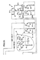
- Fig. 7 illustrates a circuit of a programmable logic array which is in accordance with the present invention.
- PLA programmable logic array
- X gated current sources 10-1 through 10-X, where "X” is any integer greater than one. All of the details of current source 10-1 are illustrated in Figure 1; only a box is shown for current source 10-X since its internal details are the same as current sink 10-1; and a sequence of dots "" indicates the other gated current sources that lie therebetween.
- Transistor 11 has a collector connected to resistor 16, which in turn is connected to a voltage source V cc .
- transistor 12 has a collector connected to resistor 17 which in turn is connected to voltage source V cC'
- Transistors 11 and 12 also have their emitters connected to the collector of transistor 13; and transistor 13 has an emitter connected to resistor 18 which in turn is connected to ground.
- An input logic signal A 1 is applied to the base of transistor 11; and reference voltages (not shown) are applied to the respective bases of transistors 13 and 12.
- transistor 11 When input logic signal A 1 is high, transistor 11 turns on so a current I C5 flows through transistor 11 while no current flows through transistor 12. Consequently, the voltage on the collector of transistor 11 is relatively low while the voltage at the collector of transistor 12 is relatively high. Conversely, when input signal A 1 is low, transistor 11 turns off while transistor 12 turns on so current I C5 flows through transistor 12 while no current flows through transistor 11. In that state, the voltage on the collector of transistor 12 is relatively low while the voltage on the collector of transistor 11 is relatively high.
- Transistor 14 has a collector connected to voltage V cc and a base connected to the collector of transistor 12. Also, transistor 15 has a collector connected to voltage V cc and a base connected to the collector of transistor 11. Those transistors 14 and 15 turn on when the voltage on their respective bases is relatively high; and they turn off when the voltage on their respective bases is relatively low. Thus, transistor 14 supplies a current from its emitter when input signal A 1 is high; while transistor 15 supplies a current from its emitter when input signal A 1 is low. Also included in the Figure 1 PLA is an array 20 of conductors, diodes, and fuses. A total of "X" row conductor pairs are in the array; and a total of "Y" column conductors are in the array where "Y" is any integer greater than one. In Fig. 1 the row conductor pairs are indicated by reference numerals 21-1 through 21-X; while the column conductors are indicated by reference numerals 22-1 through 22-Y.
- Each row conductor in a row conductor pair respectively connects to the emitter of one of the transistors 14 and 15. Thus, current flows in one row conductor or the other a pair of depending upon the state of the input logic signal. Then, at each location where a row conductor crosses a column conductor, a serially interconnected diode-fuse 23 is provided to selectively couple current from the row conductors to the column conductors.
- Circuit 30 which is coupled to conductors 21-1 through 22-Y. Circuit 30 operates to generate respective NAND logic signals indicating when current is received by the various column conductors. Circuit 30 includes a total of Y transistors 31-1 through 31-Y, and a total of Y resistors 32-1 through 32-Y. Each column conductor connects to the collector of a respective transistor; that transmitter's emitter connects to a respective resistor; the base of all of the transistors 31-1 through 31-Y connect to a reference voltage (not shown); and all the resistors connect to ground.
- circuit 30 One preferred modification to circuit 30 is indicated by reference numeral 40.
- the Y column conductors are partitioned into several groups of N. For example, fifty column conductors might be partitioned into ten groups of five. Those N column conductors respectively couple to the collector of transistors 41-1 through 41-N. Transistors 41-1 through 41-N then have their emitters all connected together; and they in turn connect to a single resistor 42. Resistor 42 has a resistance which equals that of one of the resistors 32-1 through 32-Y divided by N. Consequently, by choosing an appropriate value for N, the resistance of resistor 42 is made nearly identical to the resistance of resistor 18 in the gated current sources.
- All of the above-described circuitry operates to form respective NAND logic signals on column conductors 22-1 through 22-Y.
- the voltage on column conductors 22-1 is to represent the logical NAND of input signals A 1 and A x .
- the voltage on column conductor 22-1 must be low whenever input signal A 1 is high and input signal A x is simultaneously low.
- the voltage on column conductor 22-1 must be high whenever input signal A 1 is low or input signal A x is high.
- circuitry that remains to be described in Figure 1 is similar to that which was described above.
- that remaining circuit includes another plurality of gated current sources 10'-1 through 10'-Y which are similar to gated current sources 10-1 through 10-X, an array 20' which is similar to array 20, and an output circuit 30' which is similar to circuits 30 and 40.
- Each of the gated current sources 10 /- 1 through 10'-Y includes four transistors 11', 12', 13', and 15'; and three resistors 16', 17', and 18'.
- the transistors and resistors in gated current source 10'-1 have the same number, except for the "prime", as their counterpart in the previously described gated current source 10-1.
- transistor 15' corresponds to transistor 15.
- each of the row conductors, column conductors, and diode-fuse combinations in array 20' has the same number except for a "prime” as the number of its counterpart in array 20. That is, row conductors in array 20' are indicated by reference numerals 21'-1 through 21'-Y; the column conductors are indicated by reference numerals 22'-1 through 22'-Z where "Z" is any integer; and diode-fuse combinations are indicated by reference numeral 23'.
- each of the components in output circuit 30' has the same reference numeral except for the "prime” as its counterpart in circuit 30.
- the transistor and resistor pair that couple to column 22'-1 to form an output signal are labeled 31'-1 and 32'-1.
- transistors 11' in the gated current sources 0'-1 through 10'-Y respectively couple via their base to column conductors 22-1 through 22-Y to receive respective NAND terms therefrom. So, a low on any one of the column conductors 22-1 through 22-Y will cause current to flow in the corresponding row conductors 21'-1 through 21'-Y; and the output voltage on column conductor 22'-1 goes high when current is coupled thereto from any one of the row conductors 21'-1 through 21'-Y.
- the above components with primed reference numerals operate to form output signals which are the logical NAND of selected NAND terms on column conductors 22-1 through 22-Y.
- the output signal on column conductor 22'-1 is to represent the NAND of the terms on column conductors 22-1 and 22-Y. That is achieved by not blowing the fuses that couple column conductor 22'-1 to row conductors 21'-1 and 21'-Y, while at the same time blowing the fuses that couple column conductor 22'-1 to all the remaining row conductors.
- Figure 1 PLA One feature of the Figure 1 PLA is that it uses substantially less power than PLA's of the prior art. Also, another feature of the Figure PLA is that it occupies substantially less chip space than PLA's of the prior art. To understand how that is so, reference should now be made to the prior art PLA of Figure 2.
- Each gated current sink includes five transistors 51-55, a single resistor 56, and a diode 57.
- Transistors 51 and 52 have their bases and collectors connected to the cathode of diode 57 which in turn has its anode connected to a voltage supply V cc .
- Transistor 51 has its emitter connected to the collector of transistor 53; and transistor 52 has its emitter connected to the collector of transistor 54.
- Transistors 53 and 54 have their emitters connected to the collector of transistor 55 which in turn has its emitter connected to resistor 56 which then connects to ground.
- the base of transistor 53 in each of the gated current sinks 50-1 through 50-X is coupled to receive a respective input logic signal A 1 through A X ; and the base of transistor 54 is coupled to a reference voltage (not shown).
- a reference voltage not shown.
- FIG. 6 Also included in the PLA of Figure 2 is an array 60 of row conductor pairs, column conductors, and diode-fuse interconnections.
- Reference numerals 61-1 through 61-X indicate the row conductor pairs; reference numerals 62-1 through 62-Y indicate the column conductors; and reference numeral 63 indicates the diode-fuse interconnections.
- Pullup resistors 64-1 through 64-Y respectively couple the column conductors to supply voltage V cc
- logical "AND" terms are formed on column conductors 62-1 through 62-Y.
- the signal on column conductor 62-1 is to represent the "AND" term of signals A 1 and A x .
- the signal on column conductor 62-1 must be high whenever signal A, is high and simultaneously signal A X is low; or conversely, the signal on column conductors 62-1 must be low whenever A 1 is low or A X is high.
- Transistor 54 in current sink 50-1 will sink current from the row conductor to which it connects when input signal A, is low; while transistor 53 in current sink 50-X will sink current from the row conductor to which it connects when input signal Ax is high. Consequently, the fuse that couples column conductor 62-1 to transistor 54 in current sink 50-1 should not be blown; the fuse that couples column conductor 62-1 to transistor 53 in current sink 50-X should not be blown; and all of the remaining fuses that couple column conductor 62-1 to the row conductors should be blown.
- PLA is an array 70 of transistors. This array has Y columns, Z rows, and a transistor at each row-column intersection.
- the column conductors are indicated by reference numerals 62-1 through 62-Y; the row conductors are indicated by reference numerals 71-1 through 71-Z; and the transistors are indicated by reference numerals 72.
- Each transistor 72 has its collector connected to voltage source V cc , has its base connected to one of the column conductors 62-1 through 62-Y, and has its emitter coupled through a fuse 73 to one of the row conductors 71-1 through 71-Z.
- An output circuit 80 then connects to row conductors 71-1 through 71-Z.
- Circuit 80 includes transistors 81-1 through 81-Z which have their collectors respectively connected to the row conductors 71-2 through 71-Z; and it includes resistors 82-1 through 82-Z which respectively connect the emitters of transistors 81-1 through 81-Z to ground.
- Circuit 80 generates respective output signals on row conductors 71-1 through 71-Z which represent the logical "OR” of selected "AND” terms on column conductor 62-1 through 62-Y.
- the output signal on row conductor 71-1 is to represent the "OR” of the "AND” terms on column conductor 62-1 and 62-Y.
- the voltage on row conductor 71-1 must be high whenever the voltage on column conductor 62-1 or 62-Y is high. That is achieved by not blowing the fuses 73 that couple column conductors 62-1 and 62-Y to row conductor 71-1, while simultaneously blowing the fuses 72 that couple all of the remaining column conductors to row conductor 71-1.
- Equation 1 of Column 1 states that the current I, in any one of the row conductors of array 20 can under certain conditions equal the total current I c Y in all of the column conductors. That condition occurs, for example, when the state of the input logic signals A 1 ⁇ A x , along with the blown-not blown state of the fuses are such that one current source supplies current to all of the column conductors while the other current sources supply no current at all.
- equation 2 states that the base current I b which drives the transistor 14 (or 15) in the current source that is supplying current IY is equal to where (3 is the transistor's gain. At the same time, however, an even larger l cs must flow through transistor 11 to there cause a voltage drop which is large enough to turn off transistor 15. This is stated by equation 3. For example, current l cs may be five times as large as current I b ; and this is stated by equation 4.
- Resistors of the same order of magnitude in an integrated circuit are made by merely adjusting the resistors' physical dimensions while using the same steps of the IC manufacturing process. Since the same steps are used, any variations in doping concentrations, processing temperatures, etc. will be the same for all of the resistors that are formed. Thus, if the process variations are such as to cause one resistance to increase, it will also cause the other resistances to increase, and vice versa.
- Resistors 18 and 32-1 through 32-Y are of the same order of magnitude; so the ratio of those resistors in any particular chip will not vary by any significant amount from their desired ratio of one-fifth.
- equation 7 states that Further, by using circuit 40 in Figure 1, the magnitude of resistor 18 can be made nearly identical to the magnitude of resistors 32-1 through 32-Y. This is stated by equation 8.
- equation 1 gives an expression for the current l cs through resistor 56 under the conditions where the current l c in all of the column conductors is being passed to a single row conductor. Under such conditions, current l cs equals Y times the column conductor current l c plus an additional current IT which flows through transistor 52.
- resistors 56 and 64-1 through 64-Y differ substantially from each other, it is impractical to make them from the same steps of a manufacturing process by merely adjusting their physical dimensions. Instead, resistors 56 and 64-1 through 64-Y must be made by separate sets of steps; so consequently, the ratio of any two particular resistors can vary substantially from the ratio of their average value. This is stated by equation 5.
- the value R cs of resistor 56 could be at its average value R cs while at the same time the value R of resistors 64-1 through 64-Y could be at only eight-tenths (8/10) of their average value R.
- the value of current l cs would be at its average value Î cs while the value of the column currents I c would be twenty percent (20%) larger than their average value Î c .
- the average value of current l cs must be at least as large as 1.2I c Y. This is stated by equation 8. Otherwise, the PLA would not even work since under the above conditions the current sinks 50-1 through 50-X would not be able to sink all of the column conductor current.
- current I C5 is also made up of a current IT which flows through transistor 52.
- Current IT will be at a minimum when current I c Y is at a maximum since current I C5 is essentially a constant. That minimal value of current IT will be approximately one-tenth (1/10) of current I cs . This is stated by equation 9. Consequently, as stated by equation 10, current Ics must be at least 1.3 times column conductor current times Y.
- equation 1 there gives the ratio of equation 11 in Column 1 to equation 13 in Column 2. Inspection of this power ratio shows that the current sources of Figure 1 dissipate only approximately one-fourteenth (1/ 14) the power that is dissipated by the current sinks of Figure 2.
- equation 2 gives an expression for the average power that is dissipated in the entire PLA of Figure 1.
- the leftmost term is the average power dissipated in current sources 10-1 through 10-X; the next term is the average power dissipated in array 20; the next term is the average power dissipated in current sinks 10'-1 through 10'-Y; and the last term is the average power dissipated in array 20'.
- equation 3 gives the average power that is dissipated in the entire PLA of Figure 2.
- the leftmost term is the average power dissipated by current sinks 50-1 through 50-X; the next term gives the average power dissipated in array 60; and the last term gives the average power dissipated by array 70.
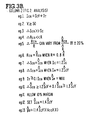
- equation 2 can be simplified to include only the first and third term while equation 3 can be simplifed to include only the first term. Then, to obtain the ratio of the power that is dissipated in the Figure 1 PLA to the power that is dissipated in the Figure 2 PLA, the above simplified equation 2 needs only to be divided by the simplified equation 3. This result is expressed as equation 4.
- Equation 1 of Column 1 states the number of transistors in all of the current sources 10-1 through 10-X. There are five transistors 11-15 in each of those current sources; and so the total number of transistors equals 5X. Equation 2 then states the total number of diodes in array 20 of the Figure 1 PLA. That array has 2X rows and Y columns, and so the total number of diodes is 2XY.
- equation 7 an expression can be written for the total area occupied by the Figure 1 PLA. That expression is given as equation 7. There, a symbol AT represents the area required by a single transistor, and a symbol A D represents the area required by a single diode.
- Equation 1 gives the total number of transistors in current sinks 50-1 through 50-X; equation 2 gives the total number of diodes in the current sinks 50-1 through 50-X; equation 3 gives the total number of diodes in array 60; equation 4 gives the total number of transistors in array 70; and equation 5 gives the total number of transistors in output circuit 80. Equations 1-5 are . then combined as equation 6 to give an expression for the total area required by the Figure 2 PLA. Symbols AT and A D again respectively represent the area occupied by one transistor and one diode.
- Equation 1 in Column 3 compares equation 7 of Column 1 with equation 6 of Column 2. Both of the terms AT and A D are included in equation 1; and area AT always is substantially greater than area Ap. For example, AT will be ten times A D ; and this is stated by equation 2. Substituting equation 2 into equation 1 then gives an expression for the ratio of the area occupied by the Figure 1 PLA to the area occupied by the Figure 2 PLA. This is given by equation 3.
- Each row-column pair in the Figure 5 table has two entries.
- the top entry gives the range for X within which equation 3 will be less than one; and the bottom entry evaluates equation 3 under the condition where X equals 30.
- equation 3 will be less than one for all values of X that are greater than or equal to six; and equation 3 will equal when X equals 30.
- the area occupied by the Figure 2 PLA is 2.297 times as large as the area occupied by the Figure 1 PLA.
- the number X of input signals in a PLA is at least 20, and so inspection of Figure 5 shows that equation 3 will be less than one for all practical values of X.
- Figure 6A is a schematic diagram of the input signal current sources and diode array of the embodiment of Figure 1.
- Reference numerals 10-1 through 10-X again indicate the current sources
- reference numerals 21-1 through 21-X again indicate the row conductor pairs
- reference numerals 22-1 through 22-Y again indicate the column conductors.
- Equation 1 of Figure 6A also gives an expression for the power that is dissipated in the illustrated portion of the PLA. That power was derived previously as equation 11 of Column 1 in Figure 3.
- Each of the column conductors 22-1 through 22-Y has a parasitic capacitance associated with it. This capacitance was indicated as C o in Figure 6A. But in Figure 6B, the length of the column conductors must double since the number of row conductor pairs doubles. Consequently, in Figure 6B, two parasitic capacitances of C o are associated with each of the column conductors.
- a column conductor capacitance must be discharged whenever the voltage on that conductor goes from a high to a low level; and the amount of charge Q that is required to produce a voltage change V across the capacitance is given in Figure 6B as equation 1. That charge Q will be discharged as the current I from the column conductors to circuit 30; and its magnitude equals the magnitude of current I times the time At in which current I flows. This is stated by equation 2. Utilizing equations 1 and 2, the amount of time At which it takes to discharge the column conductor parasitic capacitors can be stated as equation 3.
- the circuit of Figure 6C the number of input signals has been expanded to mX.
- the circuit includes mX input current sources 10-1 through 10-mX, mX row conductor pairs 21-1 through 21-mX, and Y column conductors 22-1 through 22-Y.
- the length of each of those column conductors is m times the length of the column conductors in Figure 6A; and consequently their parasitic capacitance is m times C o .
- Figure 7A dissipiates substantially less power than the circuit of Figure 6C; yet it receives the same number of input signals and operates at the same speed as the Figure 6C circuit.
- included in the Figure 7A embodiment are a total of mX current sources 10-1 through 10-mX. Those mX current sources are partitioned into m groups with each group including a total of X current sources, and each group having its own set of column conductors.
- the first group of current sources 10-1 through 10-X has row conductors 21-11 through 21-X1 and column conductors 22-11 through 22-Y1; ...; and the last group of current sources has row conductors 21-1m through 21-Xm and column conductors 22-1m through 22-Ym. Since each of the column conductors 22-11 through 22-Ym is associated with only X row conductor pairs, its length will be the same as the length of the column conductors of Figure 6A; so consequently it will have a parasitic capacitance of Co.
- Each of the m groups of column conductors respectively couples to one of the previously described circuits 30.
- reference numeral 30-1 indicates the first of those circuits whereas reference numeral 30-m indicates the last of those circuits.
- Corresponding column conductors in each of the m groups couple to the base of respective transistors which in turn have their emitters connected to another column conductor and their collectors connected to voltage source V cc .
- all of the rightmost column conductors 22-Y1 through 22-Ym couple to the base of respective transistors 90-Y1 through 90-Ym; the emitter of those transistors connect to a column conductor 91-Y; and the collector of those transistors connects to voltage source V cc .
- the total time required to receive an output signal from the Figure 7A circuit equals the time ⁇ t1 required to discharge one capacitor C o plus the time ⁇ t2 required to discharge one capacitor C'. This is stated in Figure 7B as equation 1. Also, as stated previously, the time At to discharge a capacitance equals and substituting this relation into equation 1 yields equation 2.
- column conductors 22-11 through 22-Ym are made of patterned diffusions in a semiconductor substrate; row conductors 21-11 through 21-Xm are made of patterned metal lines which lie on an insulating layer over the substrate; and the interconnecting diodes 23 (not shown) are Schottky diodes that are formed by contacts between the patterned metal lines and patterned diffusions.
- column conductors 91-1 through 91-Y are made of a patterned second level metal layer which lies on an insulating layer over the patterned metal layer that forms the row conductors.
- capacitance C o can be broken into the floor capacitance of the diffusion plus two times the sidewall capacitance of the diffusion. This is stated by equation 3.
- Those capacitances will vary from process to process; but a typical floor capacitance of a diffusion is 0.10 fF/D and a typical sidewall capacitance for diffusion is 0.40 fF/O.
- equation 4 the parasitic capacitance of a patterned metal layer will vary from process to process; but a typical value for such parasitic capacitance is 0.025 fF/O. This is stated by equation 5.
- a typical capacitance ratio of a diffusion capacitor to a metal on an insulating layer capacitor is approximately 30:1.
- capacitor C' is approximately one-thirtieth (1/30) capacitor C o . So if the current I' that discharges capacitor C' is made equal to the current 1 0 that discharges capacitor C o , then the total charge time for the Figure 7A embodiment will approximately equal ⁇ t 1 . This is stated by equation 7.
- equation 8 gives an expression for the power dissipated by each group of X current sources in the Figure 7A circuit.
- symbol P1 represents the power dissipated by the first group of current sources
- symbol P2 represents the power dissipated by the second group of current sources, etc.
- power was previously derived as P. in equation 11 of Column 1 of Figure 3.
- equation 9 states that the total power dissipated by all of the Figure 7A current sources is mP a .
- equation 10 gives an expression for the power dissipated by the column conductor circuitry in Figure 7A.
- the rightmost term is the power dissipated by that circuitry which carries current I'; and the next term is the power dissipated by that circuitry which carries current I c .
- Inspection of equation 10 shows that both of those terms are insignificant to mP o when current I' equals current I c and the number of input terms mX is much larger than one.
- the power expressed by the second term is identical to the power dissipated in the array of Figure 6C, so that term will cancel out in a comparison of the two PLA's.
- Equation 10 can thus be ignored in the expression for the total power dissipated for the Figure 7A circuit. And that leaves out equation 9. Then, equation 9 can be compared with equation 3 of Figure 6C; and that gives equation 11. This result shows that the power dissipated by the Figure 7A circuit is only times the power dissipated by the Figure 6C circuit, which is a substantial improvement for large values of m.
Landscapes
- Physics & Mathematics (AREA)
- Mathematical Physics (AREA)
- Engineering & Computer Science (AREA)
- Computer Hardware Design (AREA)
- Computing Systems (AREA)
- General Engineering & Computer Science (AREA)
- Logic Circuits (AREA)
- Design And Manufacture Of Integrated Circuits (AREA)
Claims (8)
Applications Claiming Priority (2)
| Application Number | Priority Date | Filing Date | Title |
|---|---|---|---|
| US06/436,374 US4506173A (en) | 1982-10-25 | 1982-10-25 | Low power partitioned PLA |
| US436374 | 1982-10-25 |
Publications (2)
| Publication Number | Publication Date |
|---|---|
| EP0110550A1 EP0110550A1 (de) | 1984-06-13 |
| EP0110550B1 true EP0110550B1 (de) | 1986-08-13 |
Family
ID=23732147
Family Applications (1)
| Application Number | Title | Priority Date | Filing Date |
|---|---|---|---|
| EP83306478A Expired EP0110550B1 (de) | 1982-10-25 | 1983-10-25 | Unterteilte, programmierbare logische Anordnung mit niedrigem Leistungsverbrauch |
Country Status (5)
| Country | Link |
|---|---|
| US (1) | US4506173A (de) |
| EP (1) | EP0110550B1 (de) |
| JP (1) | JPS59132243A (de) |
| CA (1) | CA1192626A (de) |
| DE (1) | DE3365334D1 (de) |
Families Citing this family (14)
| Publication number | Priority date | Publication date | Assignee | Title |
|---|---|---|---|---|
| US4554640A (en) * | 1984-01-30 | 1985-11-19 | Monolithic Memories, Inc. | Programmable array logic circuit with shared product terms |
| US4645953A (en) * | 1984-07-03 | 1987-02-24 | Monolithic Memories, Inc. | Current source which saves power in programmable logic array circuitry |
| US5021689A (en) * | 1989-01-19 | 1991-06-04 | National Semiconductor Corp. | Multiple page programmable logic architecture |
| US4942319A (en) * | 1989-01-19 | 1990-07-17 | National Semiconductor Corp. | Multiple page programmable logic architecture |
| US5081375A (en) * | 1989-01-19 | 1992-01-14 | National Semiconductor Corp. | Method for operating a multiple page programmable logic device |
| US5055712A (en) * | 1990-04-05 | 1991-10-08 | National Semiconductor Corp. | Register file with programmable control, decode and/or data manipulation |
| JPH04249423A (ja) * | 1991-02-06 | 1992-09-04 | Nec Corp | マスタースライス型ecl回路 |
| US6314549B1 (en) * | 1998-01-09 | 2001-11-06 | Jeng-Jye Shau | Power saving methods for programmable logic arrays |
| MXPA06015184A (es) | 2004-06-23 | 2007-11-22 | Nestec Sa | Procedimiento y composiciones utiles para prevenir y/o tratar pieles sensibles y/o secas. |
| FR2920304B1 (fr) | 2007-09-04 | 2010-06-25 | Oreal | Utilisation cosmetique de lysat bifidobacterium species pour le traitement de la secheresse. |
| FR2920305B1 (fr) | 2007-09-04 | 2010-07-30 | Oreal | Utilisation d'un lysat de bifidobacterium species pour le traitement de peaux sensibles. |
| US8438522B1 (en) | 2008-09-24 | 2013-05-07 | Iowa State University Research Foundation, Inc. | Logic element architecture for generic logic chains in programmable devices |
| US8661394B1 (en) | 2008-09-24 | 2014-02-25 | Iowa State University Research Foundation, Inc. | Depth-optimal mapping of logic chains in reconfigurable fabrics |
| FR2942719B1 (fr) | 2009-03-04 | 2011-08-19 | Oreal | Utilisation de microorganismes probiotiques pour limiter les irritations cutanees |
Family Cites Families (3)
| Publication number | Priority date | Publication date | Assignee | Title |
|---|---|---|---|---|
| US3818252A (en) * | 1971-12-20 | 1974-06-18 | Hitachi Ltd | Universal logical integrated circuit |
| JPS5631137A (en) * | 1979-08-22 | 1981-03-28 | Fujitsu Ltd | Decoder circuit |
| US4433331A (en) * | 1981-12-14 | 1984-02-21 | Bell Telephone Laboratories, Incorporated | Programmable logic array interconnection matrix |
-
1982
- 1982-10-25 US US06/436,374 patent/US4506173A/en not_active Expired - Lifetime
-
1983
- 1983-10-21 JP JP58198193A patent/JPS59132243A/ja active Granted
- 1983-10-21 CA CA000439502A patent/CA1192626A/en not_active Expired
- 1983-10-25 EP EP83306478A patent/EP0110550B1/de not_active Expired
- 1983-10-25 DE DE8383306478T patent/DE3365334D1/de not_active Expired
Also Published As
| Publication number | Publication date |
|---|---|
| EP0110550A1 (de) | 1984-06-13 |
| JPH0430768B2 (de) | 1992-05-22 |
| DE3365334D1 (en) | 1986-09-18 |
| JPS59132243A (ja) | 1984-07-30 |
| US4506173A (en) | 1985-03-19 |
| CA1192626A (en) | 1985-08-27 |
Similar Documents
| Publication | Publication Date | Title |
|---|---|---|
| US4506173A (en) | Low power partitioned PLA | |
| US5053909A (en) | Semiconductor integrated circuit device | |
| US4347446A (en) | Emitter coupled logic circuit with active pull-down | |
| US4554640A (en) | Programmable array logic circuit with shared product terms | |
| EP0109777B1 (de) | Programmierbare logische Anordnung mit niedrigem Leistungsverbrauch und kleinem Flächenbedarf | |
| US4511914A (en) | Power bus routing for providing noise isolation in gate arrays | |
| US5378941A (en) | Bipolar transistor MOS transistor hybrid semiconductor integrated circuit device | |
| US4683384A (en) | Integrated circuit having input and output drivers cascaded between I/O pads and internal circuitry | |
| US4677317A (en) | High voltage signal output circuit provided with low voltage drive signal processing stages | |
| US5083181A (en) | Semiconductor integrated circuit device and wiring method thereof | |
| US4891729A (en) | Semiconductor integrated-circuit apparatus | |
| US4801820A (en) | LSI array having power down capability | |
| WO1993017500A1 (en) | Differential ecl circuit | |
| US4593205A (en) | Macrocell array having an on-chip clock generator | |
| US4644191A (en) | Programmable array logic with shared product terms | |
| EP0011961A1 (de) | Dreizustandsausgangsstufe | |
| US6031982A (en) | Layout design of integrated circuit, especially datapath circuitry, using function cells formed with fixed basic cell and configurable interconnect networks | |
| US5066996A (en) | Channelless gate array with a shared bipolar transistor | |
| US4239981A (en) | Fast semiconductor digital logic inverter gate | |
| US5491431A (en) | Logic module core cell for gate arrays | |
| KR100280951B1 (ko) | 출력 전류 변동을 억합할 수 있는 전류 출력형 디지털-아날로그 변환기 | |
| US5841723A (en) | Method and apparatus for programming anti-fuses using an isolated well programming circuit | |
| EP0121424B1 (de) | LSI-Vorrichtung für eine Toranordnung | |
| US3281607A (en) | Nand nor logic circuit for use in a binary comparator | |
| EP0025667B1 (de) | Logische Schaltungsvorrichtung |
Legal Events
| Date | Code | Title | Description |
|---|---|---|---|
| PUAI | Public reference made under article 153(3) epc to a published international application that has entered the european phase |
Free format text: ORIGINAL CODE: 0009012 |
|
| 17P | Request for examination filed |
Effective date: 19831029 |
|
| AK | Designated contracting states |
Designated state(s): BE DE FR GB NL SE |
|
| GRAA | (expected) grant |
Free format text: ORIGINAL CODE: 0009210 |
|
| AK | Designated contracting states |
Kind code of ref document: B1 Designated state(s): BE DE FR GB NL SE |
|
| REF | Corresponds to: |
Ref document number: 3365334 Country of ref document: DE Date of ref document: 19860918 |
|
| ET | Fr: translation filed | ||
| RAP2 | Party data changed (patent owner data changed or rights of a patent transferred) |
Owner name: BURROUGHS CORPORATION (A DELAWARE CORPORATION) |
|
| BECN | Be: change of holder's name |
Effective date: 19860813 |
|
| NLT2 | Nl: modifications (of names), taken from the european patent patent bulletin |
Owner name: BURROUGHS CORPORATION TE DETROIT, MICHIGAN, VER. S |
|
| PLBE | No opposition filed within time limit |
Free format text: ORIGINAL CODE: 0009261 |
|
| STAA | Information on the status of an ep patent application or granted ep patent |
Free format text: STATUS: NO OPPOSITION FILED WITHIN TIME LIMIT |
|
| 26N | No opposition filed | ||
| PGFP | Annual fee paid to national office [announced via postgrant information from national office to epo] |
Ref country code: BE Payment date: 19921116 Year of fee payment: 10 |
|
| PG25 | Lapsed in a contracting state [announced via postgrant information from national office to epo] |
Ref country code: BE Effective date: 19931031 |
|
| BERE | Be: lapsed |
Owner name: BURROUGHS CORP. Effective date: 19931031 |
|
| PGFP | Annual fee paid to national office [announced via postgrant information from national office to epo] |
Ref country code: SE Payment date: 19940916 Year of fee payment: 12 |
|
| PGFP | Annual fee paid to national office [announced via postgrant information from national office to epo] |
Ref country code: NL Payment date: 19941031 Year of fee payment: 12 |
|
| EAL | Se: european patent in force in sweden |
Ref document number: 83306478.5 |
|
| PG25 | Lapsed in a contracting state [announced via postgrant information from national office to epo] |
Ref country code: SE Effective date: 19951026 |
|
| PG25 | Lapsed in a contracting state [announced via postgrant information from national office to epo] |
Ref country code: NL Effective date: 19960501 |
|
| EUG | Se: european patent has lapsed |
Ref document number: 83306478.5 |
|
| NLV4 | Nl: lapsed or anulled due to non-payment of the annual fee |
Effective date: 19960501 |
|
| REG | Reference to a national code |
Ref country code: GB Ref legal event code: IF02 |
|
| PGFP | Annual fee paid to national office [announced via postgrant information from national office to epo] |
Ref country code: GB Payment date: 20020913 Year of fee payment: 20 |
|
| PGFP | Annual fee paid to national office [announced via postgrant information from national office to epo] |
Ref country code: FR Payment date: 20021003 Year of fee payment: 20 |
|
| PGFP | Annual fee paid to national office [announced via postgrant information from national office to epo] |
Ref country code: DE Payment date: 20021031 Year of fee payment: 20 |
|
| PG25 | Lapsed in a contracting state [announced via postgrant information from national office to epo] |
Ref country code: GB Free format text: LAPSE BECAUSE OF EXPIRATION OF PROTECTION Effective date: 20031024 |
|
| REG | Reference to a national code |
Ref country code: GB Ref legal event code: PE20 |