EP0108674A1 - Graphisches Terminal mit Punktspeicher, ausgerüstet mit einem System zum Schreiben von Bildgewebesignalen in einen Bildspeicher - Google Patents
Graphisches Terminal mit Punktspeicher, ausgerüstet mit einem System zum Schreiben von Bildgewebesignalen in einen Bildspeicher Download PDFInfo
- Publication number
- EP0108674A1 EP0108674A1 EP83402066A EP83402066A EP0108674A1 EP 0108674 A1 EP0108674 A1 EP 0108674A1 EP 83402066 A EP83402066 A EP 83402066A EP 83402066 A EP83402066 A EP 83402066A EP 0108674 A1 EP0108674 A1 EP 0108674A1
- Authority
- EP
- European Patent Office
- Prior art keywords
- circuit
- memory
- output
- pattern
- input
- Prior art date
- Legal status (The legal status is an assumption and is not a legal conclusion. Google has not performed a legal analysis and makes no representation as to the accuracy of the status listed.)
- Granted
Links
Images


Classifications
-
- G—PHYSICS
- G06—COMPUTING; CALCULATING OR COUNTING
- G06T—IMAGE DATA PROCESSING OR GENERATION, IN GENERAL
- G06T11/00—2D [Two Dimensional] image generation
- G06T11/001—Texturing; Colouring; Generation of texture or colour
Definitions
- the subject of the present invention is a graphics terminal with point memory provided with a system for writing image texture signals into image memory.
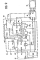
- FIG. 1 A graphic terminal with point memory is shown very generally in FIG. 1. It comprises a management microcomputer 10, a control circuit 12, an image memory 14, a video signal generator 16 connected to the memory and finally a video display receiver 18.
- the circuit 12 is schematically composed of a memory address generator (designated by the abbreviation GAM) and a plan selector (designated by SP).
- GAM memory address generator
- SP plan selector
- Figure 2 shows the structure of these elements and the various connections that connect them.
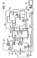
- the image memory 14 with its N memory planes 14 1 ... 14 N (N being an integer at least equal to 1), each plane comprising a matrix set of points suitable for each store a bit or bit. Each point is defined by an address.
- the N bits of the N points having the same address in the different planes define a word of N bits which will be denoted subsequently V.
- the memory 14 has an address input l4Ad common to the N planes and a control input 14C also common to all plans; it also has N validation inputs 14V 1 ... 14V N and N binary outputs 14S 1 ... 14S N.
- the control circuit 12 comprises a sequencer 20 and a graphic display processor 22.
- the sequencer has a clock output 20si and control outputs 20s 2 .
- the graphic display processor has an input 22e, a first output group 22s 1 associated with the outputs 20s 2 of the sequencer, these outputs delivering control signals denoted SC defining a memory access cycle, a second group of outputs 22s 2 , delivering address signals denoted SAd, a third group of outputs 22s 3 delivering clock signals SH and synchronization intended for the generator 16.
- the control signals SC are applied, by a first bus, to the control input 14C of memory 14 and the address signals SAd, by a second bus, at the address input l4Ad.
- the control circuit 12 also includes a circuit 24 which is connected to N gates 26 1 ... 26 N , the outputs of which are connected to the validation inputs 14V 1 ... 14V N of the memory.
- the circuit 24 controls the opening of the doors 26 1 ... 26 N to validate the memory plans according to the signal delivered by the output 22si of the circuit 22.
- circuit 12 fulfill the function of memory address generation (GAM) and selection of planes (SP).
- the video signal generator 16 has N binary inputs 16e 1 ... l6e N connected to the N binary outputs of the image memory 14, a synchronization input 16E connected to the third group of outputs 22s 3 of the graphic display processor 22 and a clock input 16H connected to the clock output 20s 1 of the sequencer 20.
- the generator 16 also has an output 16s delivering video (R, G, B) and synchronization (S) signals.
- a graphic terminal of this kind has the function of generating images from information it receives or processes. These images are constructed and stored point by point in the memory 14 which is for this reason called "image memory".
- image memory The management of such a graphic terminal is ensured by the microcomputer 10 which dialogues with the outside (in practice with a host computer, another terminal, a keyboard, a graphic tablet, etc.) and transforms creation requests. images as appropriate signals, which are delivered on its output 10si and addressed to the control circuit 12.
- the latter is designed so that the values corresponding to each of the points constituting the graphics to be displayed are written in image memory. These values reflect the appearance of each of the points as they should appear on the screen: it may be the luminance, primary colors or any other quantity making it possible to restore one or the other of these characteristics.
- a definition of the skeleton of the graphic which is obtained by the definition of a set of points and an evaluation, for each of the points of the skeleton, of the value V which will represent it in image memory.
- the first operation is carried out by the memory address generator GAM, which generates addresses, in other words point coordinates, the second by the plan selector SP.
- the value V entered is one of 2 N possible values and it results in a word of N bits formed of binary elements equal to 0 or 1.
- Each "1" having a determined rank in the word is stored in the memory map of the same rank at the address defined by the address generator.
- the role of the video generator 16 is to convert the signal read from the image memory into a signal capable of controlling a display member such as a video receiver. Typically, this signal is of the type encountered in television. Note that the video generator 16 has read, permanent access to the image memory.
- circuit 12 of image memory 14 and of generator 16 constitutes what is called a viewing tomato.
- design of such automata was essentially based on software which was used to define the operations necessary for the display of characters, points, vectors, arcs, circles, spots, etc.
- the disadvantage of these devices is that they lead to a relatively long run time. For this reason, certain functions linked in particular to the image memory and to the video generator, have been the subject of some hardware improvements so that the processing of the plot generator is accelerated.
- a second generation of display automata appeared with the development of integrated circuits specialized in the management of image memories defined by points (for example the EFCIS 9365 or NEC 7220 circuits). These circuits group together, in general, the functions of global memory management, for the account of the writing trace generator and for that of the video generator in reading, of management of the memory itself (dynamic memory refresh); they also provide the functions of structuring the video signal (synchronization, erasure period) and a few tracing functions (of characters, segments, arcs, etc.). However, such circuits only work with a single memory plane. They are characterized especially by a great speed-execution of the plots, but by a less fine control of the graphics obtained.
- the terminal specially designed for telegraphy or alphageometric videography, which is the subject of French patent application No. 2,465,281 entitled "Digital transmission and transmission device". display of graphics and / or characters on a screen ".
- the write accesses of the image memory are under the control of the software, which fully determines each point to be written and its value.
- the GAM and SP functions mentioned above are then obtained by instruction programs. It is possible to implement, with such a terminal, a process known as area filling, in order to cover part of the image with hatching or to give it a particular shade.
- the share of software is lower and that of hardware higher.
- the integrated circuits used are capable of performing high level management of the image memory.
- the EF 9365 graphic display processor developed by EFCIS directly generates characters or vectors in image memory at high speed. In this case, however, we no longer control the appearance of the displayed points as finely, because this type of circuit does not know the concept of memory planes.
- the purpose of the present invention is precisely to reconcile the flexibility of solutions based on software and the speed of specialized hardware while seeking relative simplicity of implementation.
- the invention provides for the insertion, in a terminal of the kind of that just described, of a system for writing image texture signals into image memory, which, like the shows FIG. 3, where it bears the reference 30, is inserted between, on the one hand, the sequencer group 20 and the graphic display processor 22 and, on the other hand, the memory 14.
- a system for writing image texture signals into image memory which, like the shows FIG. 3, where it bears the reference 30, is inserted between, on the one hand, the sequencer group 20 and the graphic display processor 22 and, on the other hand, the memory 14.
- Such a system is designed so that it is possible to write to the image memory at a speed which is compatible with the use of specialized circuits.
- a terminal equipped with the system of the invention has two operating modes: a "normal” mode, which is that where the value V assigned to different points is constant, programmable and independent of the position of the points, and a " pattern ", which is where the value V assigned to a point is a function of the position of the point in the pattern that we want to obtain.
- the first mode is used in the case of vector plots, display of characters or areas with a uniform background and the second in the case of plots of areas with a non-uniform background (for example in the case of hatching).
- the system of the invention is based on textures which are obtained by repeating the same pattern. Also, the speed of access to the image memory is independent of the pattern used, of the desired texture or of the number of planes of the image memory.
- the system of the invention requires operation of the image memory and of the generator memory addresses such that all bits of the same address are accessed simultaneously in the N planes, by a memory write cycle.
- the visual rendering of each point of the image memory is controlled, the specialized circuit serving as memory address generator being used at its maximum speed.
- This punctual access makes it possible, by having the system of the invention treat only the points inside an area, to automatically solve the problem of cutting the texture along the outline of this area.
- the results which can be obtained according to the invention are particularly characteristic in the case where it is necessary to fill portions of the image with different textures.
- the terminal uses a memory with a single plane, capable of memorizing an image with two luminance levels, it is possible, thanks to the invention, to simulate several luminance levels by the use of different patterns with variable point density.
- this technique can be generalized in order to artificially widen the palette of colors.
- a matrix of image memory points, L lines and E columns is called a "pattern".
- This motif is inscribed in a mesh which is a rectangle with sides AX and AY.
- Such a mesh can be repeated according to the principle illustrated in FIGS. 4a and 4b.
- the mesh In the horizontal direction, the mesh repeats with the period AX and shifts vertically by AV (figure 4a).
- the mesh In the vertical direction, the mesh repeats with the period AY, shifting horizontally from A H ( Figure 4b).
- the vertical offset and the horizontal offset are mutually exclusive, that is to say that if AH is not zero, then AV is (figure 4b) and vice versa (figure 4a) .
- an origin of the mesh which is the point corresponding to the lower left corner of the elementary starting pattern. Its contact details will be noted off x and offy.
- a mesh is thus composed of two parts: the pattern part which contains different points distributed in the dotted rectangles in FIGS. 4a and 4b, and the mesh bottom part which includes the complementary zones.
- the points forming the mesh background can correspond to a chosen constant value, which then generates a uniform background, or correspond to the value which characterized the appearance of the screen before the introduction of the pattern, the mesh background then being transparent.
- FIG. 5 This is what is represented in FIG. 5, where the left part shows an aspect of the screen corresponding to an image before incorporating an image texture and, on the right part the aspect of this screen for a mesh with uniform bottom (top) and transparent bottom (bottom).
- An image texture corresponding to such a repeating pattern is written to image memory according to the following process.
- Knowing a and ⁇ it remains to determine whether the point is in the pattern part or in the pattern background part. This amounts to examining whether a is less than E and if, simultaneously, ⁇ is less than L. If this condition is satisfied (condition which will be denoted subsequently by the notation "IN") the memory point of coordinates (x, y) corresponds to a point located in the pattern . A word defined by the pattern corresponds to it in the image memory. If this condition is not satisfied, the memory point (x, y) corresponds to a point located out of the pattern and the word which corresponds to it will remain unchanged in the event of transparent mesh background or will take an arbitrary value in the event of background of uniform mesh.
- Figures 6, 7 and 8 illustrate some textures that can be obtained with different combinations of values AX, AY, AH and AV.
- the shape and the repetition mode of the stitch are schematized by four white rectangles (in practice obviously, the repetition of the elementary pattern extends over more than four stitches).
- the shape of a mesh is defined by A X and AY (cf. Figures 4a, 4b) and the offset of a mesh during its repetition is defined by AH and AV.
- FIG. 9 shows, by way of example, a combination of textures which can be obtained by the system of the invention. Naturally, all of these examples have no limiting character, but are only intended to illustrate the principle of the generation of a texture which is the basis of the invention.
- the pattern memory circuit comprises a first memory assigned to dot patterns, a second memory assigned to skeleton patterns and a third memory assigned to true patterns; to these memories are added a logic pattern selection circuit and a multiplexer delivering the word corresponding to the pattern selected in the chosen type.
- mesh parameters AX, AY, AH and AV numbers which are powers of 2.
- the operations division and product intervening in relations (1) and (1 ') above, boil down to binary element shifts, and the "modulo" functions of relations (2), (3), (2 ') and (3') are simple to perform.
- relations (2) and (3) or (2 ') and (3') can be achieved by the same circuits as for positive numbers.
- This very simple principle is used to deal with relations (2) and (2 '). It can also be when ⁇ * (or ⁇ *) is negative, which corresponds to relations (3) or (3 '). Thus, is it not necessary, in this particular case, to analyze beforehand the sign of a (or ⁇ *) to obtain a (or ⁇ ).
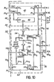
- the system for writing image texture signals into image memory which in FIG. 5 has the reference 30, is represented in a synoptic manner in FIG. 10.
- This system essentially comprises two parts: a part 40 , for processing the access cycle to the image memory and a part 50 for determining the word to be written in memory. These two parts will be described in turn.
- the operation of the system shown in Figure 10 is as follows. First of all, being inserted between the address generator and the image memory, it behaves towards the first, like an image memory and towards the second, like a address generator. To compensate for the processing time inherent in the system itself, the first part 40 (composed of circuits 41 and 42) transmits to the image memory the signals it receives (SC and SAd) from the address generator with a delay constant (hence SC * and SAd *). The first function of the system 30 is therefore a delay function which is fulfilled by the circuit 41. The second function of this first part of the system is to reconstruct, from the address signals SAd supplied by the address generator, the coordinates (x, y) of the current point. This is the role assigned to circuit 42. The second part 50 essentially has the function of translating the coordinates (x, y) provided by part 40, into a word V intended to be written in image memory, according to modalities defined in advance. It is this part 50 which implements the texture generation process described above.
- the circuit 42 interprets the address signals SAd to deliver a pair of coordinates (x, y) stable during the operation of the part 50.
- the circuit 54 transforms the coordinates x, y of the current point it receives from the shaping circuit 42, into relative coordinates ⁇ , ⁇ and uses for this the characteristics of the mesh and of the dimensions of the pattern as illustrated in FIGS. 4a and 4b. It furthermore elaborates for the selection circuit 56, the logic signal "IN".
- the pattern memory circuit 55 has information relating to several types of patterns. This information is supplied to it by the microcomputer but it can also be inherent in a particular design of the storage system (use of read only memories).
- the description of a stitch pattern consists of a choice of a particular value.
- the description of a skeleton motif requires a matrix of points, each element of which is identified by an index k which fixes the value of the element according to a pre-established table.
- the description of a true pattern requires a complete matrix of which each element can take a particular value.
- the circuit 55 receives from the configuration circuit 53 logic information which makes it possible to select one of the three types of possible patterns and, in this type, a particular pattern. Knowing this pattern and the couple a, P, the circuit 55 is capable of supplying the selection circuit 56 with the value V M of the word to be written in memory for the point considered.
- circuit 56 validates the writing cycle in progress and definitively selects the value (V) to be written in image memory, depending on the operating mode chosen (Normal / Pattern, Uniform / Transparent) . For this it receives from the parameter circuit 53 the information concerning this mode as well as the value V F ′ and from the pattern memory 55, the value V M as well as the logic signal DANS produced by the circuit 54. Table I below after describes the operation of this circuit by showing in which case the writing in image memory is blocked (ie in "Pattern" mode when the point is not in the pattern and the background is transparent): and which of the words V F and V M is transmitted to the image memory; (V M is transmitted only in "Pattern” mode when the treated point is in the pattern).
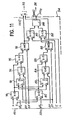
- circuits 54, 55 and 56 will now be described with the aid of FIGS. 11, 12 and 13.
- FIG. 11 first of all, represents the diagram of a circuit 54 for calculating a and ⁇ operating according to the principle described above, in the case where the different quantities defining the mesh are powers of 2.
- the circuit comprises two analogous channels, the first comprising an adder 70 with two inputs receiving x and off x , a divider 72 receiving AY and the result of the addition carried out by the adder 80, a multiplier 74 receiving AH and the result of the division carried out by the divider 72, a subtractor 76 connected to 70 and 74, a circuit 78 fulfilling the modulo AX function and receiving for this AX and the result of the subtraction carried out by the subtractor 76; the second channel comprises identical circuits, namely an adder 80, a divider 82, a multiplier 84, a subtractor 86, a circuit 88 for calculating modulo A Y.
- the first way delivers, as it results directly from the equations given above, the coordinate a and the second way the coordinate ⁇ .
- the circuit 54 also comprises a first comparator 90 receiving a and E, a second comparator 92 receiving ⁇ and L and an AND 94 logic gate which delivers the signal DANS.
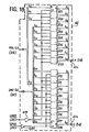
- FIG. 12 represents a particular embodiment of a pattern memory circuit. As shown, this circuit includes a pattern-point memory circuit 101, a pattern-skeleton memory circuit 111 and a pattern-true memory circuit 131.
- the pattern-point memory circuit 101 comprises a plurality of n memories 100 1 ... 100 n , each memory having an input connected to the second output 10s 2 of the computer 10. These memories contain values Vp 1 ... Vp n .
- the circuit further comprises a multiplexer 102 having n inputs 102e l ... 102e each connected to one of the n memories 100 1 ... 100 n , a control input 102C and an output 102s delivering a signal Vp.
- the skeleton pattern memory circuit 111 comprises a memory 110 formed by several memory planes, each plan having a validation input 112, one in loading port l13 connected to the second output 10s 2 of the computer 10 and an addressing input 114 connected to the output 54si of the circuit 54. These memory planes have a common output 116.
- the circuit also comprises a plurality of n ' memories 120 1 ... 120 n ,, n 'being an integer at least equal to 1, each containing a particular word Vs i ... Vs n ,.
- the circuit finally comprises a multiplexer 122 with n 'inputs 122e 1 ... 122e n ', each connected to one of the memories 120 1 ... 120 n , with a control input 122C connected to the common output 116 of the memory 110 and at an output 122s delivering a word Vs characterizing the selected skeleton pattern.
- the true pattern memory circuit 131 comprises a memory 130 formed of planes each consisting of a matrix of memory points, each plane of this memory 130 having a validation input 132, a loading input 133 connected to the second output group 10s2 of the computer 10, an addressing input 134 connected to the output 54s 1 of the calculation circuit 54 and a single output 136 delivering a Vv specific to the selected pattern.
- the pattern memory circuit 55 includes a logic circuit selection 138 having an input 138e connected to the second output 53s 2 of the operating parameterization circuit 53 and receiving a signal determining the choice of a pattern, a first output 138s, delivering a signal determining a pattern, this output being connected to the control input 102C of the multiplexer 102 of the pattern-point memory circuit 101 as well as to the input 112 of validation of one of the memory plans of the memory 110 of the pattern-skeleton memory circuit 111, as well as that at the input 132 for validating one of the memory plans of the memory 130 of the true pattern memory circuit 131; circuit 138 also has a second output 138s 2 delivering a signal determining the type of pattern selected (pattern-point, pattern-skeleton, pattern-true).
- circuit 55 includes a multiplexer 140 with three inputs 140e l , 140e 2 , 140e 3 connected to the outputs of the pattern memory circuits 101, 111, 131, to a control input 140C connected to the second output 138s 2 of the logic circuit. selection 138 and to an output 140s delivering the selected word V M taken from Vp, Vs and Vv. This output 140s constitutes the output 55s of the global pattern memory circuit, which is connected to the second input 56e 2 of the selection circuit 56.
- the operation of this circuit is as follows.
- the signals applied to the decoding logic 150 control the multiplexer 152 which delivers either V M or V F , the selected word being stored in 156 at the start of the delayed write cycle.
- the output 56s 1 delivers the write control signal from the image memory and the output 56s 2 the word V to be written.
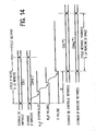
- FIG. 14 gives the operating diagram of the overall system 30.
- the control (SC) and address (SAd) signals appear on the first two lines.
- the next two lines show the appearance of the signals x, y and a, ⁇ .
- the fifth line corresponds to the availability of the word V to be written in memory. This word V is available with a delay t compared to the start of the writing cycle.
- the control and address signals (SC * , SAd) must then be applied to the image memory with this delay. .
- Figures 15 and following relate to a particular embodiment of the system which has just been described.
- the characteristics of this system are as follows: the graphics processor 22 is the circuit 9365 GDP of EFCIS, which will be designated subsequently by its initials GDP (for "Graphic Display Processor”); the microcomputer is organized around a CPU 6800; the image memory is formed by three planes of 512 ⁇ 512 bits each, produced in dynamic memory (circuits of the type EF 4116); each plane is assigned a primary color of the video signal (red, green or blue); the plots are made at high speed (1 point is defined and written in less than 2 us).
- the operating instructions for the EF 9365 circuit gives details of the operation of this circuit and specifies the form of the various signals it delivers (D W , DI N , DAD, MSL, ALL, DOUT, SYNC).
- the sequencer 20 delivers, for its part, the various clock signals necessary: a signal CK for the GDP, two signals HRAS, HCAS for the dynamic memories and a clock signal CK 'for the video generator.
- This sequencer is controlled by a 14 MHz oscillator.
- the image memory consists of three identical planes each consisting of 16 EF 4116 boxes.
- One plane receives the address signals, the signal.
- DW write / read
- DIN 1 , DIN 2 or DIN 3 a validation signal DIN 1 , DIN 2 or DIN 3 according to its rank.
- the video generator controlled by the sequencer, formats the synchronization signal (SYNC) produced by the GDP, and works out from the DOUT signal, three primary color signals R, G and B.
- SYNC synchronization signal
- the dimensions E and L of the patterns are fixed at the system definition for the skeleton patterns and the true patterns, and programmable, within the respective limits of AX and AY, in the point pattern.
- Table IV gives two examples of true patterns composed of colored patterns, the first of two-color nested squares and the second of a triangle on a colored background.
- Table V gives the correspondence between the value of the elements in Table IV and the primary colors R, G, B.
- the memory cycle transmission circuit 41 is illustrated in FIG. 17. It comprises 16 delay lines (for example of the DDU-3J-5500 type, providing a delay of 400 ns), respectively 170, 172, 174 (6 grouped lines ), 176 (4 grouped lines), 178, 180 and 182.
- the address signals DAD 0-6, MSL 0-3 and control ALL DW, DIN coming from the GDP 22 on the one hand and BRAS and HCAS coming from the sequencer 20 on the other hand, are delayed by these lines by same duration (in this case 400 ns).
- the 14 delayed signals thus obtained, DAD 0-6 * , MSL 0-3 * , and ALL * are sent to memory 14.
- the start of cycle signals DCy * , pen (P1 * ) and write ture (Ec * ) (see Figures 10 and 13) intended for circuit 56 consist respectively of the signals HRAS * , DIN * and DW * .
- FIG. 18 An embodiment of the circuit 42 for shaping x, y is shown in FIG. 18. It includes 18 D flip-flops of type 74S175 respectively 201 to 218 and two inverters 219, 220. Each flip-flop has two inputs D and CP and an output Q. The inputs D receive the address signals MSL 0-3 and DAD 0-6 coming from the GDP 22 and the inputs Q the signals BRAS and HCAS, applied through the inverters 219, 220. Thus the signals are sampled address as soon as they are issued by the GDP. Table II mentioned above fixes the correspondence between the signals MSL and DAD on the one hand and the bits of the coordinates x and y on the other hand. After the downward transition from HCAS, the two values x and y are available on outputs 42s.
- FIGS. 19a and 19b A particular embodiment of the operating parameterization circuit 53 is shown in FIGS. 19a and 19b.
- the part shown in FIG. 19a comprises 12 flip-flops D (of type 74LS175) referenced from 230 to 241, two AND gates of type 74LS11 referenced respectively 242 and 243 and two NAND gates of type 7400 referenced respectively 244 and 245.
- a bus 221, from the microcomputer 10, delivers bits to the flip-flops defining the different operating characteristics defined by the bytes described above.
- Connection 222 controls the loading of MODE byte
- connection 225 loads the MESH byte.
- the two connections 223 and 224 which are respectively the MOTIF-SQ outputs of 257 and MOTIF-VR of 258 each validate the two outputs of 235 and 236 to obtain respectively AX 32 by gate 242 and AY 32 by gate 243.
- the part shown in FIG. 19b comprises 18 D flip-flops of type 74LS175, referenced 251 to 268 and four AND gates of type 7408 referenced 270 to 273.
- These flip-flops and gates are supplied by the data bus 221 and by connections 226 for loading the MOTIF byte, 227 for loading the DIME byte, 227 ′ loading of the DIML byte, 228 and 228 'are respectively the validations of the two most significant binary elements of E and L, that is to say outputs of 262 and 263 for 228 and outputs of 267 and 268 for 228 '.
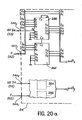
- Figures 20a to 20d illustrate a particular embodiment of the circuit 54 for calculating a and ⁇ . Carried out in combinatorial logic, this circuit performs the calculations corresponding to relations (1), (2) and (3) and (1 '), (2') and (3 ') given above, from the values x and y supplied by circuit 42 according to the mesh defined by circuit 53 using AX, AY, AH, AV, off x and offy.
- the circuit of FIG. 20a comprises two adders 280, 282, for example of the type 74283, receiving offX4 (coming from 237, figure 19a) and x and two adders 284, 286 receiving offY4 (coming from 238, figure 19a) and y. It delivers x + off x and y + off.
- the circuit of FIG. 20b comprises a first set of four multiplexers 290 to 293 and a second similar set of four other multiplexers 295 to 298 (shown diagrammatically in the upper right). All these circuits are for example of the 74S151 type. They include three control inputs S 0 , S 1 and S 2 .
- the first set of multiplexers receives x + off x from circuits 280 and 282 in FIG. 20a as well as AX32, AY32, AV2, AVO coming from gates 242, 243 of flip-flop 239 and gate 245 of circuit 53 (FIG. 19a ).
- the second set receives analogously y + offy and AY32, AX32, AH2, AHO.
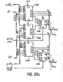
- the circuit of FIG. 20c comprises three adders 300, 302, 304, for example of the type 74283, which receive KX and KY coming from the circuits of FIGS. 20b, as well as x + off x and y + offy coming from the circuits of FIG. 20a.
- the circuit of FIG. 20c further comprises two circuits 306 and 308, of type 74157, used to perform the modulo operation (AX or AY) and receiving AX32 and AY32 coming from circuit 53 (FIG. 19a).
- the set delivers the coordinates a and ⁇ on the outputs 54s ,, which are applied to the circuit 55.
- the circuit illustrated in FIG. 20d comprises two comparators 310 and 312 of type 9324, receiving a and E for the first and ⁇ and L for the second.
- FIG. 21 A particular embodiment of the circuit 55 of "pattern memory” is represented in FIG. 21. It includes a read-only memory 320, for example of the type 6301, three multiplexers 322, 324 and 326, three logic AND gates 321, 323 and 325, for example of type 74 S08 .
- the circuit 55 receives the signal Vp coming from the circuit 53, the coordinates a and ⁇ coming from the circuit 54, the pattern number on the input 55e 3 and the signals MOTIF-VR and MOTIF-SQ coming from 53. It delivers the value V m associated with the point ⁇ , ⁇ for the motif considered.
- the signal Vp supplied by the configuration circuit 53, is sent directly to the inputs I 0 of the output multiplexers 324 and 326.
- the multiplexers 324 and 326 receive on the inputs I 1 the value Vp validated by the address element (a, ⁇ ) through the AND gates.
- the value of the element to be written is sent to the inputs I 2 and I 3 of the final multiplexers 324 and 326.
- the eight skeleton patterns and the two true patterns are stored in memory 320 with addresses A 0 to A 7 in accordance with Table VII below:
- bit b 2 is applied to input A 6 of the memory 320 and the bits b 0 and b 1 on the inputs S 0 , S 1 of the multiplexer 322 which is of the type 4 ⁇ 1.
- the binary element b 2 applied to input A6 of 320 selects a group from two, of four skeleton patterns: skeleton patterns 0, 1, 2, 3 or skeleton patterns 4, 5, 6, 7.
- skeleton patterns 0, 1, 2, 3 or skeleton patterns 4, 5, 6, 7.
- the correspondence between the patterns and the outputs O 0 , O 1 , 0 2 and 0 3 of the memory 320 is indicated in table VIII below.
- One of the four patterns in a group is definitively selected by the multiplexer 322 controlled by the bits b 0 and b l .
- input A 7 of the memory is used and its three outputs, 0 0 (for blue), O 1 (for green) and 0 2 (for red) are only taken into account, 0 3 being ignored.
- FIG. 22 A particular embodiment of the circuit 56 for "selection of the configuration" is illustrated in FIG. 22. It comprises a multiplexer 330, for example of the 74S175 type, receiving V F and V M , four flip-flops 340 to 343, of the 74S175 type , inverters 331, 332, 334, 335, type 74S04, one AND gate 333 of type 74S08, one NAND gate 336 of type 74S10, one NAND gate 337 of type 74SOO, and three NAND doors of outlet 346, 347, 348 of type 74SOO.
- a multiplexer 330 for example of the 74S175 type, receiving V F and V M , four flip-flops 340 to 343, of the 74S175 type , inverters 331, 332, 334, 335, type 74S04, one AND gate 333 of type 74S08, one NAND gate 336 of type 74S10, one NAND gate 337 of type
- This circuit selects the final value V and blocks writing to image memory in accordance with table I already mentioned.
- the multiplexer 330 receiving V F and V M coming respectively from the setting circuits 53 and from the pattern memory 55, is controlled by the control signal DANS-ET-MOTIF which validates V M.
- the selected value is then memorized by the complement signal of HRAS * in flip-flops 340, 341, 342; the output of these flip-flops being validated by the complement of DIN * through doors 346, 347, 348.
- the three signals DIN 0 , DIN 1 , and DIN 2 of output are sent to them in validation inputs 14V ,, 14V 2 , 14V 3 of the three planes of the image memory.
- the second part of circuit 56 creates a write signal DW M to the image memory, according to the logical relation:
- This write signal is stored in flip-flop 343 at the same time as the value V selected in flip-flops 340 to 342.
- the timing diagrams relating to the embodiment which has just been described are shown in Figures 23 and 24.
- the timing diagram of Figure 23 first of all, relates to the read and refresh cycles of the image memory.
- the GDP initiates a reading cycle of the image memory, on behalf of the video generator, or a refresh cycle of the dynamic memories, such a cycle is transmitted as it is to the image memory with a delay of 400 ns . Since it receives no write request, it ignores the three signals DIN 0 , DIN 1 , DIN 2 which, although generated by the system 30, are meaningless (this is the meaning of the dotted line of the DIN lines on the timing diagram of FIG. 23). Except for the time difference, the system 30, in such a cycle, is therefore transparent.
- the timing diagram of FIG. 24 relates to the writing cycle.
- the coordinates (x, y) of the current point are given in the three address blocks at 0 , ⁇ 1 , ⁇ 2 , sampled by HRAS and HCAS so that they are frozen at the output of the shaping circuit of x, y (42).
- the coordinates (x, y) are valid approximately 17 ns after the descent of HCAS.
- the signals ⁇ , ⁇ are available approximately 120 ns after and the logic signal DANS approximately 150 ns after the availability of (x, y).
- V m from (a, ⁇ ), at the output of the pattern memory circuit 55 takes the longest to take place in the case of a skeleton pattern. In this case, she asks for 90 ns.
- the memorization in the circuit 56 of selection of the signal DW and of the DIN O to 2 by the signal HRAS * may occur 200 ns after the low transition of HCAS.
- HRAS and HC A S it can be considered that 400 ns is an acceptable value of the delay to be imposed on the signals of the memory cycle, before applying them to the image memory.
- FIG. 25 is a timing diagram illustrating the internal functioning of the system of the invention and which highlights the maximum duration of execution in the case of skeleton patterns.
- the writing cycle as just described relates to the processing of a current point of a given texture.
- the microcomputer of the terminal loads the 5 bytes of command MODE, MESH, PATTERN, DIME and DIML, then launches the display of the points involved in this texture.
Landscapes
- Physics & Mathematics (AREA)
- General Physics & Mathematics (AREA)
- Engineering & Computer Science (AREA)
- Theoretical Computer Science (AREA)
- Image Generation (AREA)
- Controls And Circuits For Display Device (AREA)
Applications Claiming Priority (2)
| Application Number | Priority Date | Filing Date | Title |
|---|---|---|---|
| FR8218492A FR2535871B1 (fr) | 1982-11-04 | 1982-11-04 | Terminal graphique a memoire de points muni d'un systeme d'ecriture en memoire d'image de signaux de texture d'image |
| FR8218492 | 1982-11-04 |
Publications (2)
| Publication Number | Publication Date |
|---|---|
| EP0108674A1 true EP0108674A1 (de) | 1984-05-16 |
| EP0108674B1 EP0108674B1 (de) | 1987-06-03 |
Family
ID=9278894
Family Applications (1)
| Application Number | Title | Priority Date | Filing Date |
|---|---|---|---|
| EP83402066A Expired EP0108674B1 (de) | 1982-11-04 | 1983-10-24 | Graphisches Terminal mit Punktspeicher, ausgerüstet mit einem System zum Schreiben von Bildgewebesignalen in einen Bildspeicher |
Country Status (7)
| Country | Link |
|---|---|
| US (1) | US4543645A (de) |
| EP (1) | EP0108674B1 (de) |
| JP (1) | JPS59133588A (de) |
| BR (1) | BR8306053A (de) |
| CA (1) | CA1222840A (de) |
| DE (1) | DE3371949D1 (de) |
| FR (1) | FR2535871B1 (de) |
Cited By (1)
| Publication number | Priority date | Publication date | Assignee | Title |
|---|---|---|---|---|
| EP0164457A1 (de) * | 1983-04-12 | 1985-12-18 | The Marconi Company Limited | Bilderzeugungsgerät |
Families Citing this family (12)
| Publication number | Priority date | Publication date | Assignee | Title |
|---|---|---|---|---|
| FR2566949B1 (fr) * | 1984-06-29 | 1986-12-26 | Texas Instruments France | Systeme d'affichage d'images video sur un ecran a balayage ligne par ligne et point par point |
| GB8507988D0 (en) * | 1985-03-27 | 1985-05-01 | Sigmex Ltd | Raster graphical display apparatus |
| US5129060A (en) * | 1987-09-14 | 1992-07-07 | Visual Information Technologies, Inc. | High speed image processing computer |
| US4985848A (en) * | 1987-09-14 | 1991-01-15 | Visual Information Technologies, Inc. | High speed image processing system using separate data processor and address generator |
| US5109348A (en) * | 1987-09-14 | 1992-04-28 | Visual Information Technologies, Inc. | High speed image processing computer |
| US5146592A (en) * | 1987-09-14 | 1992-09-08 | Visual Information Technologies, Inc. | High speed image processing computer with overlapping windows-div |
| US4998214A (en) * | 1989-04-03 | 1991-03-05 | Unisys Corp. | Apparatus for line imaging |
| US5027551A (en) * | 1990-02-28 | 1991-07-02 | Rodriguez Lazaro E | Decorative lawn edging package |
| US5293480A (en) * | 1990-08-06 | 1994-03-08 | At&T Bell Laboratories | High resolution graphics system architecture |
| US5230039A (en) * | 1991-02-19 | 1993-07-20 | Silicon Graphics, Inc. | Texture range controls for improved texture mapping |
| US6002407A (en) | 1997-12-16 | 1999-12-14 | Oak Technology, Inc. | Cache memory and method for use in generating computer graphics texture |
| US7880711B1 (en) * | 2007-04-30 | 2011-02-01 | Lockheed Martin Corporation | Image stability in liquid crystal displays |
Citations (3)
| Publication number | Priority date | Publication date | Assignee | Title |
|---|---|---|---|---|
| US3999308A (en) * | 1975-03-12 | 1976-12-28 | The Singer Company | Real-time simulation of a point system having textured areas as viewed by a moving observer |
| US4225861A (en) * | 1978-12-18 | 1980-09-30 | International Business Machines Corporation | Method and means for texture display in raster scanned color graphic |
| FR2466061A1 (fr) * | 1979-06-15 | 1981-03-27 | Redifon Simulation Ltd | Perfectionnement aux systemes de visualisation du type a image engendree par calculateur |
-
1982
- 1982-11-04 FR FR8218492A patent/FR2535871B1/fr not_active Expired
-
1983
- 1983-10-24 EP EP83402066A patent/EP0108674B1/de not_active Expired
- 1983-10-24 DE DE8383402066T patent/DE3371949D1/de not_active Expired
- 1983-10-31 CA CA000440035A patent/CA1222840A/en not_active Expired
- 1983-11-01 US US06/547,778 patent/US4543645A/en not_active Expired - Fee Related
- 1983-11-03 BR BR8306053A patent/BR8306053A/pt unknown
- 1983-11-04 JP JP58206072A patent/JPS59133588A/ja active Pending
Patent Citations (3)
| Publication number | Priority date | Publication date | Assignee | Title |
|---|---|---|---|---|
| US3999308A (en) * | 1975-03-12 | 1976-12-28 | The Singer Company | Real-time simulation of a point system having textured areas as viewed by a moving observer |
| US4225861A (en) * | 1978-12-18 | 1980-09-30 | International Business Machines Corporation | Method and means for texture display in raster scanned color graphic |
| FR2466061A1 (fr) * | 1979-06-15 | 1981-03-27 | Redifon Simulation Ltd | Perfectionnement aux systemes de visualisation du type a image engendree par calculateur |
Cited By (1)
| Publication number | Priority date | Publication date | Assignee | Title |
|---|---|---|---|---|
| EP0164457A1 (de) * | 1983-04-12 | 1985-12-18 | The Marconi Company Limited | Bilderzeugungsgerät |
Also Published As
| Publication number | Publication date |
|---|---|
| US4543645A (en) | 1985-09-24 |
| BR8306053A (pt) | 1984-06-12 |
| JPS59133588A (ja) | 1984-07-31 |
| DE3371949D1 (en) | 1987-07-09 |
| FR2535871B1 (fr) | 1987-06-19 |
| EP0108674B1 (de) | 1987-06-03 |
| FR2535871A1 (fr) | 1984-05-11 |
| CA1222840A (en) | 1987-06-09 |
Similar Documents
| Publication | Publication Date | Title |
|---|---|---|
| EP0108674B1 (de) | Graphisches Terminal mit Punktspeicher, ausgerüstet mit einem System zum Schreiben von Bildgewebesignalen in einen Bildspeicher | |
| FR2599873A1 (fr) | Systeme d'affichage video | |
| EP0215510B1 (de) | Verarbeitungsgerät zur Beseitigung von verborgenen Seiten für dreidimensionale Bilderzeugung | |
| EP0323302B1 (de) | Verfahren zur dreidimensionalen Anzeige von digitalen achtästigen kodierten Objekten | |
| FR2583541A1 (fr) | Tampon z a haute vitesse munie d'une memoire dynamique a acces aleatoire | |
| FR2604019A1 (fr) | Dispositif d'affichage video couleur pour systeme d'ordinateur, et procede de conversion de signaux video couleur a cet effet | |
| FR2544898A1 (fr) | Dispositif d'affichage video sur ecran d'affichage par balayage d'une trame ligne par ligne et point par point | |
| FR2566950A1 (fr) | Processeur de points d'images video, systeme de visualisation en comportant application et procede pour sa mise en oeuvre | |
| CA2104807A1 (fr) | Procede de creation d'images animees | |
| FR2964236A1 (fr) | Dispositif et procede de generation d'images multifenetres a priorite variable | |
| FR2566949A1 (fr) | Systeme d'affichage d'images video sur un ecran a balayage ligne par ligne et point par point | |
| EP0202166B1 (de) | Virtuelle Bildspeicherschaltung für vielfache Bildfenster | |
| FR2509492A1 (fr) | Appareil de commande d'acces de memoire pour microcalculateur | |
| FR2543721A1 (fr) | Dispositif de generation d'images sur un ecran dans un systeme de visualisation commande par ordinateur | |
| FR2519456A1 (fr) | Generateur d'effets graphiques | |
| US5416893A (en) | Method for displaying edging or decaling of an object in a graphics display | |
| EP0178219B1 (de) | Verfahren zur Verarbeitung von synthetischen Videobildern für Anzeige in Echtzeit und mit hoher Informationsdichte und dieses Verfahren verwendende Anordnung | |
| EP0161175B1 (de) | Einrichtung zum Modifizieren des Aspektes der Bildpunkte auf einem Bildschirm eines graphischen Anzeigegerätes | |
| EP0780796B1 (de) | Symbolisches Bildanzeigesystem und -verfahren | |
| CN113559503A (zh) | 视频生成方法、设备及计算机可读介质 | |
| FR2512234A1 (fr) | Procede de simulation de vision et dispositif pour sa mise en oeuvre | |
| Isenberg et al. | Breaking the pixel barrier | |
| EP0967588A1 (de) | Anzeigesteuergerät mit Animationsschaltung | |
| JP2001101445A (ja) | ソフトシャドーキャスティング回路 | |
| FR2735318A1 (fr) | Architecture a memoire unique centralisee pour le transfert d'images video |
Legal Events
| Date | Code | Title | Description |
|---|---|---|---|
| PUAI | Public reference made under article 153(3) epc to a published international application that has entered the european phase |
Free format text: ORIGINAL CODE: 0009012 |
|
| AK | Designated contracting states |
Designated state(s): BE CH DE GB IT LI NL SE |
|
| 17P | Request for examination filed |
Effective date: 19841030 |
|
| 17Q | First examination report despatched |
Effective date: 19860813 |
|
| GRAA | (expected) grant |
Free format text: ORIGINAL CODE: 0009210 |
|
| AK | Designated contracting states |
Kind code of ref document: B1 Designated state(s): BE CH DE GB IT LI NL SE |
|
| REF | Corresponds to: |
Ref document number: 3371949 Country of ref document: DE Date of ref document: 19870709 |
|
| ITF | It: translation for a ep patent filed |
Owner name: JACOBACCI & PERANI S.P.A. |
|
| PGFP | Annual fee paid to national office [announced via postgrant information from national office to epo] |
Ref country code: NL Payment date: 19871031 Year of fee payment: 5 |
|
| PLBE | No opposition filed within time limit |
Free format text: ORIGINAL CODE: 0009261 |
|
| STAA | Information on the status of an ep patent application or granted ep patent |
Free format text: STATUS: NO OPPOSITION FILED WITHIN TIME LIMIT |
|
| 26N | No opposition filed | ||
| PGFP | Annual fee paid to national office [announced via postgrant information from national office to epo] |
Ref country code: DE Payment date: 19880915 Year of fee payment: 6 |
|
| PG25 | Lapsed in a contracting state [announced via postgrant information from national office to epo] |
Ref country code: GB Effective date: 19891024 |
|
| PG25 | Lapsed in a contracting state [announced via postgrant information from national office to epo] |
Ref country code: SE Effective date: 19891025 |
|
| PG25 | Lapsed in a contracting state [announced via postgrant information from national office to epo] |
Ref country code: LI Effective date: 19891031 Ref country code: CH Effective date: 19891031 Ref country code: BE Effective date: 19891031 |
|
| BERE | Be: lapsed |
Owner name: TELEDIFFUSION DE FRANCE Effective date: 19891031 Owner name: VIGARIE JEAN-PIERRE Effective date: 19891031 |
|
| PG25 | Lapsed in a contracting state [announced via postgrant information from national office to epo] |
Ref country code: NL Effective date: 19900501 |
|
| NLV4 | Nl: lapsed or anulled due to non-payment of the annual fee | ||
| GBPC | Gb: european patent ceased through non-payment of renewal fee | ||
| REG | Reference to a national code |
Ref country code: CH Ref legal event code: PL |
|
| PG25 | Lapsed in a contracting state [announced via postgrant information from national office to epo] |
Ref country code: DE Effective date: 19900703 |
|
| EUG | Se: european patent has lapsed |
Ref document number: 83402066.1 Effective date: 19900706 |