EP0108408A2 - Temperature compensating voltage generator circuit - Google Patents
Temperature compensating voltage generator circuit Download PDFInfo
- Publication number
- EP0108408A2 EP0108408A2 EP83111065A EP83111065A EP0108408A2 EP 0108408 A2 EP0108408 A2 EP 0108408A2 EP 83111065 A EP83111065 A EP 83111065A EP 83111065 A EP83111065 A EP 83111065A EP 0108408 A2 EP0108408 A2 EP 0108408A2
- Authority
- EP
- European Patent Office
- Prior art keywords
- temperature
- circuit
- resistor
- voltage
- resistors
- Prior art date
- Legal status (The legal status is an assumption and is not a legal conclusion. Google has not performed a legal analysis and makes no representation as to the accuracy of the status listed.)
- Granted
Links
- 230000007423 decrease Effects 0.000 claims description 4
- 238000010586 diagram Methods 0.000 description 29
- 230000010355 oscillation Effects 0.000 description 11
- 101150014330 dfa2 gene Proteins 0.000 description 7
- 230000005669 field effect Effects 0.000 description 6
- 239000003990 capacitor Substances 0.000 description 5
- 101100329504 Mus musculus Csnka2ip gene Proteins 0.000 description 4
- 230000000694 effects Effects 0.000 description 3
- 101710170231 Antimicrobial peptide 2 Proteins 0.000 description 2
- 101000955967 Deinagkistrodon acutus Thrombin-like enzyme acutin Proteins 0.000 description 2
- 239000010453 quartz Substances 0.000 description 2
- VYPSYNLAJGMNEJ-UHFFFAOYSA-N silicon dioxide Inorganic materials O=[Si]=O VYPSYNLAJGMNEJ-UHFFFAOYSA-N 0.000 description 2
- 101710170230 Antimicrobial peptide 1 Proteins 0.000 description 1
- 208000033707 Early-onset X-linked optic atrophy Diseases 0.000 description 1
- 238000005513 bias potential Methods 0.000 description 1
- 230000003247 decreasing effect Effects 0.000 description 1
- 238000004519 manufacturing process Methods 0.000 description 1
- 239000011022 opal Substances 0.000 description 1
- 208000025019 optic atrophy 2 Diseases 0.000 description 1
- 230000010363 phase shift Effects 0.000 description 1
- 229920001296 polysiloxane Polymers 0.000 description 1
- 230000001105 regulatory effect Effects 0.000 description 1
Images


Classifications
-
- G—PHYSICS
- G05—CONTROLLING; REGULATING
- G05F—SYSTEMS FOR REGULATING ELECTRIC OR MAGNETIC VARIABLES
- G05F1/00—Automatic systems in which deviations of an electric quantity from one or more predetermined values are detected at the output of the system and fed back to a device within the system to restore the detected quantity to its predetermined value or values, i.e. retroactive systems
- G05F1/10—Regulating voltage or current
- G05F1/46—Regulating voltage or current wherein the variable actually regulated by the final control device is dc
- G05F1/462—Regulating voltage or current wherein the variable actually regulated by the final control device is dc as a function of the requirements of the load, e.g. delay, temperature, specific voltage/current characteristic
- G05F1/463—Sources providing an output which depends on temperature
-
- H—ELECTRICITY
- H03—ELECTRONIC CIRCUITRY
- H03F—AMPLIFIERS
- H03F1/00—Details of amplifiers with only discharge tubes, only semiconductor devices or only unspecified devices as amplifying elements
- H03F1/30—Modifications of amplifiers to reduce influence of variations of temperature or supply voltage or other physical parameters
- H03F1/302—Modifications of amplifiers to reduce influence of variations of temperature or supply voltage or other physical parameters in bipolar transistor amplifiers
-
- H—ELECTRICITY
- H03—ELECTRONIC CIRCUITRY
- H03L—AUTOMATIC CONTROL, STARTING, SYNCHRONISATION OR STABILISATION OF GENERATORS OF ELECTRONIC OSCILLATIONS OR PULSES
- H03L1/00—Stabilisation of generator output against variations of physical values, e.g. power supply
- H03L1/02—Stabilisation of generator output against variations of physical values, e.g. power supply against variations of temperature only
- H03L1/022—Stabilisation of generator output against variations of physical values, e.g. power supply against variations of temperature only by indirect stabilisation, i.e. by generating an electrical correction signal which is a function of the temperature
- H03L1/023—Stabilisation of generator output against variations of physical values, e.g. power supply against variations of temperature only by indirect stabilisation, i.e. by generating an electrical correction signal which is a function of the temperature by using voltage variable capacitance diodes
-
- H—ELECTRICITY
- H03—ELECTRONIC CIRCUITRY
- H03B—GENERATION OF OSCILLATIONS, DIRECTLY OR BY FREQUENCY-CHANGING, BY CIRCUITS EMPLOYING ACTIVE ELEMENTS WHICH OPERATE IN A NON-SWITCHING MANNER; GENERATION OF NOISE BY SUCH CIRCUITS
- H03B5/00—Generation of oscillations using amplifier with regenerative feedback from output to input
- H03B5/30—Generation of oscillations using amplifier with regenerative feedback from output to input with frequency-determining element being electromechanical resonator
- H03B5/32—Generation of oscillations using amplifier with regenerative feedback from output to input with frequency-determining element being electromechanical resonator being a piezoelectric resonator
- H03B5/36—Generation of oscillations using amplifier with regenerative feedback from output to input with frequency-determining element being electromechanical resonator being a piezoelectric resonator active element in amplifier being semiconductor device
- H03B5/362—Generation of oscillations using amplifier with regenerative feedback from output to input with frequency-determining element being electromechanical resonator being a piezoelectric resonator active element in amplifier being semiconductor device the amplifier being a single transistor
-
- H—ELECTRICITY
- H03—ELECTRONIC CIRCUITRY
- H03B—GENERATION OF OSCILLATIONS, DIRECTLY OR BY FREQUENCY-CHANGING, BY CIRCUITS EMPLOYING ACTIVE ELEMENTS WHICH OPERATE IN A NON-SWITCHING MANNER; GENERATION OF NOISE BY SUCH CIRCUITS
- H03B5/00—Generation of oscillations using amplifier with regenerative feedback from output to input
- H03B5/30—Generation of oscillations using amplifier with regenerative feedback from output to input with frequency-determining element being electromechanical resonator
- H03B5/32—Generation of oscillations using amplifier with regenerative feedback from output to input with frequency-determining element being electromechanical resonator being a piezoelectric resonator
- H03B5/36—Generation of oscillations using amplifier with regenerative feedback from output to input with frequency-determining element being electromechanical resonator being a piezoelectric resonator active element in amplifier being semiconductor device
- H03B5/366—Generation of oscillations using amplifier with regenerative feedback from output to input with frequency-determining element being electromechanical resonator being a piezoelectric resonator active element in amplifier being semiconductor device and comprising means for varying the frequency by a variable voltage or current
- H03B5/368—Generation of oscillations using amplifier with regenerative feedback from output to input with frequency-determining element being electromechanical resonator being a piezoelectric resonator active element in amplifier being semiconductor device and comprising means for varying the frequency by a variable voltage or current the means being voltage variable capacitance diodes
-
- Y—GENERAL TAGGING OF NEW TECHNOLOGICAL DEVELOPMENTS; GENERAL TAGGING OF CROSS-SECTIONAL TECHNOLOGIES SPANNING OVER SEVERAL SECTIONS OF THE IPC; TECHNICAL SUBJECTS COVERED BY FORMER USPC CROSS-REFERENCE ART COLLECTIONS [XRACs] AND DIGESTS
- Y10—TECHNICAL SUBJECTS COVERED BY FORMER USPC
- Y10S—TECHNICAL SUBJECTS COVERED BY FORMER USPC CROSS-REFERENCE ART COLLECTIONS [XRACs] AND DIGESTS
- Y10S323/00—Electricity: power supply or regulation systems
- Y10S323/907—Temperature compensation of semiconductor
Definitions
- the present invention relates to a temperature compensating voltage generator circuit, and more particularly to a temperature compensating voltage generator circuit used for temperature compensation of electric circuits whose electric characteristics can be controlled by a control voltage.
- the electric characteristic of an electric circuit such as a gain or an oscillation frequency of an amplifier or an oscillator changes due to the change of the temperature of the surroundings and, therefore, such an electric circuit comprises a means for temperature compensation.
- a control voltage such as a DC bias potential of an electric circuit CKT, such as an amplifier which is operated by an operating voltage V CC
- a control voltage generator circuit 'i.e., temperature compensating voltage generator circuit consisting of resistors Rl and R2 and a negative coefficient temperature sensitive resistor S
- the control voltage is changed in accordance with the change of the ambient temperature so that the electric characteristic such as the gain of the electric circuit C KT is maintained in a constant ocndition.
- the temperature characteristics of the electric circuit CKT are practically measured by using the practical circuit device and the resistors Rl and R2 and the negative temperature coefficient temperature sensitive resistor S are selected.
- the temperature characteristics of the electrical circuit CKT do not show simple or linear curves, so that the conventional means cannot effect the substantially complete temperature compensation and it takes a long time to determine the characteristic of the temperature compensating voltage generator circuit.
- the characteristics of the electrical circuit CKT has changed due to the secular variation, it is necessary to stop the operation of the electric circuit CKT in order to readjust the characteristic of the temperature compensating voltage generator circuit.
- the characteristic of the electric circuit is practically measured at various temperatures and the control voltages, i.e., the temperature compensating voltages at the measured temperatures are determined so that the characteristic of the electric circuit is equalized.
- the control voltages i.e., the temperature compensating voltages at the measured temperatures are determined so that the characteristic of the electric circuit is equalized.
- the conventional temperature compensating voltage generator it is impossible to adjust the value of the control voltage independently at various temperatures, so that the adjustment of the compensating voltage of the temperature compensating voltage generator circuit is very difficult.
- the compensating voltage is adjusted at another temperature after an adjustment of the compensating voltage at a base temperature, for example a normal temperature, the compensating voltage at the base temperature which is previously adjusted, changes.
- a temperature compensating voltage generator circuit for compensating temperature characteristics of an electric circuit whose electrical characteristic can be controlled by a control voltage, which comprises:
- Fig. 2 is a circuit, diagram which illustrates the principle of the present invention.
- a diode D and a resistor R are connected parallel with each other and a current i flows through this parallel circuit.
- the diode D is in a cut off condition so that the voltage drop V is equal to i ⁇ R and the voltage drop V can be changed by changing the resistance of the resistor R.
- the voltage drop V reaches the forward biased voltage V D , for example about 0.7 V in the case of a silicone diode, the diode D turns on and a part of the current i flows through the diode D. In this condition, the voltage drop does not change and is equal to the forward biased voltage V D even if the value of the resistance of the resistor R is changed.
- Fig. 3 illustrates a relation between the voltage drop V of the aforementioned parallel circuit and the resistance of the resistor R.
- the voltage drop V is equal to the forward biased voltage V D when the resistance of the resistor R is equal to or larger than R'.
- R' is equal to V D /i.
- the forward biased voltage V D is equal to 0.7 V and the current i is equal to 2mA.
- the resistance of the resistor R is equal to or larger than 350 ohms.
- the voltage drop V is equal to 0.7 V, and, when the resistance of the resistor R is lower than 350 ohm, the voltage drop V is equal to the product of the resistance value of the resistor R and the current value i.
- the resistor R is substituted by a negative or positive temperature coefficient temperature sensitive resistor. Therefore, in a range of the ambient temperature in which the resistance of the temperature sensitive resistor is lower than R' of Fig. 3, the voltage drop V changes in accordance with the change of the ambient temperrature. In a range of the ambient temperature in which the resistance of the temperature sensitive resistor is higher than or equal to R', the voltage drop V is approximately equal to the forward biased voltage VD and does not change even when the ambient temperature has changed.
- F ig. 4 is a circuit diagram illustrating a temperature compensating voltage generator circuit as an embodiment of the present invention.
- the circuit of Fig. 4 comprises adjustable resistors R41 through R46, positive temperature coefficient temperature sensitive resistors(hereinafter referred to as PTC resistors) P41 and P42, negative temperature coefficient temperature sensitive resistors (hereinafter referred to as NTC resistors) S41 and S42 and diodes D41 through D44.
- PTC resistors positive temperature coefficient temperature sensitive resistors
- NTC resistors negative temperature coefficient temperature sensitive resistors
- V designates the potential of a voltage source
- V designates the potential of the control voltage, i.e., the temperature compensating voltage.
- the diode D41, the PTC resistors P41 and the resistor R42 constitute a first temperature sensitive circuit
- the diode D 42, the NTC resistors S41 and the resistor R43 constitute a second temperature sensitive circuit
- the diode D43, the PTC resistor P42 and the resistor R44 constitute a third temperature sensitive circuit
- the diode D44, the NTC resistor S42 and the resistor R45 constitute a fourth temperature sensitive circuit.
- each of the PTC resistors P41 and P42 and the NTC resistors S41 and S42 of the first through the fourth temperature circuits has a larger resistance than R' of Fig. 3 at the base temperature, for example the normal temperature.
- the diodes D41 through D44 are all in a turned on condition regardless of the resistance value of the resistors R42 through R45 and the control voltage V G can be adjusted by changing the resistance of the resistors R41 and R46.
- the control voltage V is as follows.
- the resistances of the PTC resistors P41 and P42 decrease and the resistances of the NTC resistors S41 and S42 increase. Therefore, at such a lower temperature, if the resistance of the resistor R42 is adjusted so as to turn off the diode D41, a current from the voltage source flows through the PTC resistor P41 and the resistor R42. Therefore, the potential drop of the first temperature sensitive circuit becomes smaller than the forward biased voltage V D of the diode D41 and determined by the total resistance of the series connection of the PTC resistor P41 and the resistor R42. In this condition, the control voltage V G becomes higher than that of the base temperature.
- the control voltage V G becomes lower than that of the base temperature. It should be noted that, at such a lower temperature, the resistances of the NTC resistors S41 and S42 become larger and thus the voltage drop of each of the second and fourth temperature sensitive circuits is equal to the forward biased voltage V D .
- the control voltage V G can be higher or lower than that of the base temperature by adjusting the resistance of the resistor R43 or R45 of the second or fourth temperature sensitive circuit so as to turn off one of the diodes D42 and D44.
- the resistance-temperature characteristics of the PTC resistors P41 and P42 or of the NTC resistors S41 and S42 can be equal to each other or can be different from each other.
- the PTC resistors P41 and P42 and/or the NTC resistors S41 and S42 having the different resistance-temperature characteristics are used, it is also possible to generate the control voltage V determined by the difference of the resistance-temperature characteristics in the condition the diodes D41 and D43 and/or-the diodes D42 and D44 are both turned on at the same temperature.
- Fig. 5 illustrates an adjustable range of the control voltage V of the circuit in Fig. 4.
- the control voltage V at the base temperature T is adjusted to be V G1 by using the resistors R41 and R46
- the level of the control voltage at a lower temperature Tl can be adjusted by the resistor R42 or R44' and the level of the control voltage at a higher temperature Th can be ajusted by the resistor R43 or R45 within the hatched range of Fig. 5.
- the level of the control voltage V G1 at the base temperature T is not changed even when the levels of the control voltage at the lower temperature Tl and the higher temperature Th are changed. Therefore, it is possible to independently adjust the level of the control voltage at each adjusting temperature.
- the control voltage changes continuously according to the change of the ambient temperature within a range including the adjusting temperatures such as the high temperature Th and the lower temperature Tl.
- an area A is obtained by the resistance value of the resistor R42 and the resistor-temperature characteristic of the PTC resistor P41 of the first temperature sensitive circuit, and areas B , C and D are obtained by the second, third and fourth temperature sensitive circuits, respectively.
- each of the first through the fourth temperature sensitive circuits mentioned above each includes one diode which can be D41, D42, D43 or D44
- the maximum adjustable range of the voltage drop is the forward biased voltage V of each of the diodes D41 through D44.
- the maximum adjustable range of each of the temperature sensitive circuits can be expanded by using a series connection of a plurality of diodes such as D , Db and D C which is connected parallel to a series connection of the resistor R and the PTC resistor P or the NTC resistor S.
- the voltage drop of each temperature sensitive circuit can be changed in a range from 0 through 2.1 V. Practically speaking, the voltage drop of the temperature sensitive circuit of Fig. 6 does not become zero even if the resistance of the resistor R is adjusted to zero, since the resistance of the PTC resistor P or the NTC resistor S does not become zero.
- Fig. 7 illustrates another embodiment of the present invention.
- the temperature compensating voltage generator of Fig. 7 comprises adjustable resistors R70 through R73, diodes D71 and D72, PTC resistors P71 and P72 and NTC resistors S71 and S72.
- the control voltage V G at the base temperature is obtained by dividing a voltage -V by the resistors R70 and R73.
- the resistance-temperature characteristics are selected so that the resistance of each of the PTC resistors P71 and P72 and the NTC resistors S71 and S72 is large and the diodes D71 and D72 are turned on. Therefore, at the base temperature, a current flows through the resistor R73, the diodes.D72 and D71 and the resistor R70, and the control voltage V does not change even if the resistances of the resistor R71 and R72 are changed.
- the adjustment of the temperature characteristic of the circuit of Fig. 7 in a higher or lower temperature is effected by the resistors R71 and R72. For example, if the sliders of the resistors R71 and R72 are both moved to the direction of the NTC resistor S71 and the PTC resistor P71, the diode D72 is in a turned on condition both at the lower temperature and at the higher temperature and the diode D71 is in a turned off condition.
- the diode D72 is in a turned off condition both at the lower temperature and at the higher temperature. Therefore, the control voltage V of both the higher and lower temperature becomes lower than that of the base temperature.
- Fig. 8 illustrates a temperature compensating voltage generator circuit as still another embodiment of the present invention.
- the characteristic of the control voltage V G can be adjusted at three points, i.e., the base temperature, the lower temperature and the higher temperature. While in this embodiment of Fig. 8, the characteristic of the control voltage V can be adjusted at five points.
- the circuit of Fig. 8 comprises a first through an eighth temperature sensitive circuit which comprise diodes D81 through D88, resistors R81 through R88, and, P T C resistors P81 through P84 and NTC resistors S81 through S84.
- the control voltage V is adjusted by changing the resistances of resistors R80 and R89 which divides a power supply voltage -V.
- the PTC resistors P81 and P82 of the first and the third temperature sensitive circuits have different resistor-temperature characteristics and the NTC resistors S81 and S82 of the second and the fourth temperature sensitive circuits have different resistor-temperature characteristics.
- the PTC resistors P83 and P84 of the fifth and the seventh temperature sensitive circuits and the NTC resistors S83 and S84 of the sixth and the eighth temperature sensitive circuits have also different resistor-temperature characteristics. Therefore, the adjustable points of the temperature can be increased.
- the resistor-temperature characteristics of the NTC resistors and the PTC resistors of the first through the eighth temperature sensitive circuits are selected so as to turn on all the diodes D81 through D88 at the base temperature.
- the control voltage V is adjusted to a value by setting the resistances of the resistors R80 and R89 at the base temperature.
- the resistances of the resistors R83 and R87 of the third and the seventh temperature sensitive circuits are adjusted.
- the PTC resistors P81 and P83 of the first and the fifth temperature sensitive circuits are selected so that the diodes D81 and D85 are not turned off at the first low temperature and the diodes D 81 and D85 are turned off at a second low temperature which is lower than the first temperature if the resistances of the resistors R81 and R85 are decreased, for example, to zero. Therefore, at the second low temperature, the control voltage V G can be adjusted by the resistors R81 and R85 of the first and the fifth temperature sensitive circuits.
- the control voltages V G can be adjusted by the resistors R84 and R88 of the fourth and the eighth temperature sensitive circuits and, at a second high temperature which is higher than the first high temperature, the control voltage V G can be adjusted by the resistors R82 and R 86 of the second and the sixth temperature sensitive circuits.
- the NTC resistors S81 and S83 are selected so that the resistances thereof are large so as to keep the diodes D82 and D86 in a turned on condition at the first high temperature and the resistances thereof become small so as to keep the diodes D82 and D86 in a turned off condition at the second high temperature.
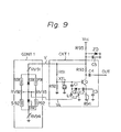
- Fig. 9 illustrates an oscillator circuit whose frequency-temperature characteristic is compensated by using the aforementioned temperature compensating voltage generator circuit of Fig. 7.
- the oscillator circuit of Fig. 9 comprises a control voltage generator CONT 1, an oscillator portion CKT1 and a decoupling circuit consisting of a zener diode ZD, a capacitor C5 and a resistor R95.
- the oscillator portion CKT1 comprises a quartz oscillator element XTL, a transistor Q, a variable capacitance diode CD, inductors L 1 and L2 capacitors Cl through C4 and resistors R91 through R94.
- the control voltage generator CONT1 has the same circuit structure as the circuit of Fig. 7 and comprises variable or adjustable resistors R V91 through RV94, diodes D91 and D92, N T C resistors S91 and S92 and PTC resistors P91 and P92.
- the oscillation frequency can be changed by the potential applied to the variable capacitor diode CD, and the potential is supplied from the control voltage generator CONT 1.
- the resistance-temperature characteristics of the NTC resistors S91 and S92 and the PTC resistors P91 and P92 are selected so that the resistance of each of these NTC resistors and the PTC resistors is large and thus a current flows through the diodes D91 and D92 and the resistors RV91 and RV94 at the base temperature for example the normal temperature of 25°C.
- the forward biased voltage of the diodes D91 and D92 is V
- the potential of the power supply voltage applied to the control voltage generator CONT 1 is V.
- the control voltage V is as follows. Therefore, at the base temperature, the control voltage V G can be adjusted by adjusting the variable resistors RV91 and/or RV94 so that the output signal having a desired frequency is obtained from an output terminal OUT.
- the oscillator portion CKT 1 has a frequency--temperature characteristic that the oscillation frequency at a high temperature which is, for example, 20°C higher than the base temperature becomes lower than that of the base temperature and the oscillation frequency at a low temperature which is, for example, 20°C lower than the base temperature also becomes lower than that of the base temperature, it is necessary to raise the oscillation frequencies at the high and the low temperature.
- the sliders of the adjustable resistors RV92 and RV93 are both adjusted to positions which are nearer to the NTC resistor S91 and the PTC resistor P91 respectively.
- the resistance of the NTC resistor S91 becomes low and the diode D91 is turned off, so that the control voltage V G becomes large in accordance with the decrease of the resistance of the NTC resistor S91.
- the temperature characteristic of the control voltage can be adjusted by the adjustable resistor RV92.
- the resistance of the PTC resistor P91 becomes low and the diode D91 is turned off, so that the control voltage V G becomes high in accordance with the decrease of the resistance of the PTC resistor P91.
- the amount of the change of the control voltage in accordance with the change of the temperature can be adjusted by the adjustable resistor RV93.
- the sliders of the adjustable resistors RV92 and RV93 are moved to positions which are nearer to the NTC resistor S92 and the PTC resistor P92 respectively.
- the control voltages at the high and the low temperature can be independently adjusted by the adjustable resistors RV92 and RV93 after the adjustment of the control voltage at the base temperature, and thus the adjustment of the control voltage V can be easily adjusted and the frequency--temperature characteristic of the oscillator circuit can be completely compensated.
- Fig. 10 is a circuit diagram illustrating another embodiment of the present invention.
- the temperature compensating voltage generator circuit of Fig. 10 comprises resistors R101 through R108, negative coefficient temperature sensitive resistor, i.e., a NTC resistor S101, a positive coefficient temperature sensitive resistor, i.e., a PTC resistor P101, diodes D101 and D102, differential amplifiers DFAl and DFA2, adjustable resistors RV101 through RV103 and an operational amplifier OPA.
- OUT designates an output terminal of the control voltage and +V and -V designate power supply voltages.
- a constant voltage from the voltage divider circuit consisting of the resistors R107 and R108 is applied and to an inverted input terminal of the operational amplifier OPA, voltages adjusted by the adjustable resistors RV101 through RV103 are applied through the resistors R103 through R105 respectively, so that the addition circuit is constituted.
- Output voltages from a voltage divider circuit consisting of the resistor R101 and the NTC resistor S101 and from another voltage divider circuit consisting of the resistor R102 and the PTC resistor P101 are respectively applied to the input terminals of the differential amplifier DFAl and DFA2 through the diodes D101 and D102, and the output voltages. from the differential amplifiers DFA1 and DFA2 are applied to the adjustable resistors RV101 and RV103 respectively.
- the resistances of the NTC resistor S101 and the resistor R101 are equal to each other and the resistances of the PTC resistor P101 and the resistor R102 are equal to each other.
- the potentials of a point a and a point b in Fig. 10 are both equal to zero and the diodes D101 and D102 are both in a cut off condition so that the output potentials of the differential amplifiers DFAl and DFA2 are both equal to zero.
- the control voltage V G from the output terminal OUT of the operational amplifier OPA is proportional to the output voltage from the adjustable resistor RV102. Therefore, at the base temperature, the control voltage V can be adjusted by the adjustable resistor RV102.
- the resistance of the NTC resistor S101 becomes smaller and the potential of the point a of Fig. 10 becomes negative, so that the diode D101 is turned on and the differential amplifier DFAl outputs a potential voltage corresponding to the potential of the point a.
- the output potential of the differential amplifier DFAl is divided by the adjustable resistor RV101 and supplied to the inverted input terminal of the operational amplifier OPA through the resistor R103 to which the potential adjusted by the adjustable resistor RV102 is supplied through the resistor R104. Therefore, at a high temperature, the control voltage V G can be adjusted by the adjustable resistor RV101.
- the resistance of the NTC resistor S101 becomes larger and the potential of the point a of Fig. 1 becomes positive so that the diode D101 is turned off and the output potential of the differential amplifier DFA1 becomes zero.
- the resistance of the PTC resistor P101 becomes smaller and the potential of the point b of Fig. 10 becomes negative so that the diode D102 is turned on and the differential amplifier DFA2 outputs a potential voltage corresponding to the potential of the point b of Fig. 10.
- the output potential from the differential amplifier DFA2 is divided by the adjustable resistor RV103 and added to the potential adjusted by the adjustable resistor RV102. Therefore, at a low temperature, the control voltage V can be adjusted by the adjustable resistor RV103.
- Fig. 11 illustrates adjustable ranges of the control voltage generated by the circuit of Fig. 10.
- the control voltage is adjusted to V G1 at the base temperature T b
- the adjustable range of the control voltage V G in a temperature range including the low temperature T a and the high temperature t b becomes an area between the solid lines of Fig. 11.
- the control voltage V at the base temperature T b is adjusted to V G2
- the adjustable range of the control voltage V G in the same temperature range becomes the area between the dotted lines of Fig. 11.
- the control voltage V G can be adjusted independently.
- Fig. 12 is a circuit diagram illustrating a temperature compensating voltage generator as another embodiment of the present invention.
- the circuit of Fig. 12 corresponds to a circuit in which the PTC resistor P101 and the resistor R102 of Fig. 10 are respectively replaced by a resistor R122 and a NTC resistor S122. It is also possible to use the NTC resistors S121 and S122 having the same resistor-temperature characteristic with each other.
- the potentials of the point a and the point b varies in accordance with the change of the ambient temperature. Therefore, after the adjustment of the control voltage by the adjustable resistor RV102 at the base temperature, the control voltages at a high temperature and at a low temperature can be independently adjusted by the adjustable resistors RV101 and RV103 respectively.
- the control voltage at the high temperature can be adjusted by the adjustable resistor RV103 and the control voltage at the low temperature can be adjusted by the adjustable resistor RV101, independently.
- the adjustable resistor RV102 used for the adjustment of the control voltages at the base temperature by a voltage divider circuit having a fixed division ratio and to connect a voltage divider circuit comprising an adjustable resistor to the non-inverted input terminal of the operational amplifier OPA, so that the control voltage at the base temperature can be adjusted by the adjustable resistor. It is also possible to invert the polarity of connection of the diodes D101 and D102.
- the adjustable resistors corresponding to the high temperature and the low temperature are replaced by each other. It is also possible to omit the diodes D101 and D102 in case the resistance-temperature characteristics of the temperature sensitive resistors used in the control voltage generator circuit are differen6"from each other.
- Fig. 13 is a circuit diagram illustrating a temperature compensating voltage generator circuit as still another embodiment of the present-invention.
- the adjustment of the characteristic of the control voltage can be effected at five points, i.e., the base temperature, a first and a second low temperature and a first and a second high temperature.
- the circuit of Fig. 13 comprises NTC resistors S131 and S132, PTC resistors P131 and P132, resistors R131 through R143, diodes D131 through D134 differential amplifiers DFAll through DFA14, adjustable or variable resistors RV131 through RV135 and an operational amplifier OPAl.
- OUT designates an output terminal of the control voltage and +V and -V designate power supply voltages.
- the resistance-temperature characteristics of the NTC resistors S131 and S132 are different from each other, or, if the resistance-temperature characteristics are the same, the resistance of the resistors R131 and R132 which are respectively connected to the NTC resistors S131 and S132 are different from each other.
- the resistance-temperature characteristics are different from each other, or, the resistance of the resistors R134 or R135 which are respectively connected to the PTC resistors P131 and P132 are different from each other. Therefore, the potentials of points a through d of Fig. 13 are different for every degree of the adjustable temperature.
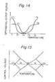
- these NTC resistors and PTC resistors are selected so that the differential output potentials V a through V d from the differential amplifiers DFA11 through DFA14 become as illustrated in Fig. 14.
- the control voltage can be adjusted by the adjustable resistor RV133.
- the control voltages can be adjusted by the adjustable resistors RV132 and RV131 respectively.
- the control voltage' can be adjusted by the adjustable resistors RV134 and RV135, respectively.
- Fig. 15 illustrates an adjustable range of the control voltage.
- the temperature characteristic of the control voltage since negative or positive voltage at each temperature t 1 , t 2 , t 4 and t 5 is added to the control voltages at the base temperature t 3 , it is also possible, for example, to adjust the temperature characteristic of the control voltage so that the control voltage at the first high temperature t 4 is higher than that at the base temperture t 3 and the control voltage at the second high temperature t 5 is lower than that at the base temperature.
- Fig. 16 is a circuit diagram illustrating a temperature compensating voltage generator circuit as still another embodiment of the present invention.
- the circuit of Fig. 16 comprises temperature sensitive circuits each comprising a series connection of a PTC resistor P161, P162, or P163 and a NTC resistor S161, S162 or S163 the circuit of Fig. 16 also comprises diodes D161 through D163, differential amplifiers DFA21 through DFA23, resistors R161 through R169, adjustable resistors RV161 through RV163 and an operational amplifier OPA2.
- OUT designates an output terminal of the control voltage and +V and -V designate power supply voltages.
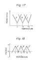
- the resistance-temperature characteristic of each series connection in each of the temperature sensitive circuits have, as illustrated by A, B or C in Fig. 17, a valley point at which the total resistance of the series connection becomes minimum and the valley points in each temperature sensitive circuit differ from each other.
- the input voltages of the differential amplifiers DFA21 through DFA23 have temperature characteristics as illustrated by A', B I and C' of Fig. 18. Therefore, at the temperatures t 1 , t 2 and t 3 , the output potentials from the differential amplifiers DFA21, DFA22 and DFA23 respectively become maximum, and the characteristic of the control voltage can be adjusted independently by the adjustable resistors RV161, RV162 and RV163 at the temperatures t 1 , t 2 and t 3 respectively.
- Fig. 19 is a circuit diagram illustrating & temperature compensating voltage generator circuit as still another embodiment of the present invention.
- the circuit of Fig. 19 comprises adjustable or variable resistors RV191 through RV193 constituting voltage dividers whose voltage division ratios are adjustable, a NTC resistor S191, a PTC resistor P191, resistors R191 through R194 and an operational amplifier OPA191.
- OUT designates an output terminal of the control voltage
- +V CC designates a power supply voltage.
- a constant voltage from a voltage divider circuit which consists of the resistors R192 and R193 and which divides the power supply voltage +V CC is applied to the non-inverted input terminal of the operational amplifier OPA191.
- the inverted input terminal of the operational amplifier OPA191 receives the voltages adjusted by the adjustable resistors RV191, RV192 and RV193 through the NTC resistor S191, the resistor R191 and the PTC resistor p191 repectively, that is, the adjusted voltages are added by the adder circuit which comprises the NTC resistor S191, the resistor R191, the PTC resistor p191, the feedback resistor R194 and the operational amplifier OPA191 and which adds the adjusted voltages under the gains corresponding to the ratio of the resistance of the NTC resistor S191, the resistor R191 and the PTC resistor P191 to the feedback resistor R194.
- the resistance of the NTC resistor S191 and the PTC resistor P191 is larger than that of the resistor R191, and thus the gain of the voltage adjusted by the adjustable resistor RV192 is larger than that of each of the voltages from the adjustable resistors RV191 and RV193. Therefore, at the base temperature, the control voltage V G can be adjusted by the adjustable resistor RV192.
- the resistance of the PTC resistor pl91 becomes smaller so that the gain of the voltage adjusted by the adjustable resistor RV193 becomes large and, therefore, the control voltage V at the low temperature can be adjusted by the adjustable resistor R193.
- the resistance of the NTC resistor S191 becomes smaller so that the gain of the voltage adjusted by the adjustable resistor RV191 becomes large and, therefore, the control voltage V G at the high temperature can be adjusted by the adjustable resistor R191.
- the adjustable range of the control voltage V G of the circuit of Fig. 19 is the same as the adjustable range illustrated in Fig. 11. As apparent from Fig. 11, if the control voltage is adjusted to V G1 at the base temperature t b , the adjustable range of the control voltage V G in the temperature range including the low temperature t a and the high temperature t c becomes the range illustrated by solid lines of Fig. 11. If the control voltage is adjusted to V G2 at the base temperature t b , the adjustable range becomes the range illustrated by the dotted lines.
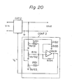
- Fig. 20 illustrates a voltage regulator system comprising the control voltage generator circuit of Fig. 19.
- a voltage regulator circuit CKT2 receives an input voltage V in and outputs a stabilized output voltage V out .
- the regulating characteristic of the voltage regulator circuit CKT2 varies in accordance with the change of the ambient temperature and thus the potential of the output voltage V out changes according to the variation of the ambient temperature.
- the control voltage i.e., temperature compensating voltage V G is applied from the control voltage generator circuit CON T 2 to the voltage regulator circuit CKT2.
- the control voltage V G is, for example, added to the error voltage of the voltage regulator circuit CKT2 detected from the output voltage V out and a reference voltage not shown in the drawing.
- F ig. 21 is a circuit diagram illustrating a temperatur e compensating voltage generator circuit as still another embodiment of the present invention.
- RV221 is an adjustable resistor and R221 and R222 are resistors.
- the control voltage V G is adjusted by the adjustable resistor RV221, and the control voltage V is proportional to the difference between the adjusted voltage from the adjustable resistor RV221 and the voltage from the voltage divider circuit consisting of the resistors R221 and R222.
- the resistance of the PTC resistor P191 becomes smaller and the voltage adjusted by the adjustable resistor RV193 is mainly added to the voltage at the base temperature.
- the resistance of the NTC resistor S191 becomes smaller and the voltage adjusted by the adjustable resistor RV191 is mainly added to the voltage at the base temperature. Therefore, after the adjustment of the control voltage V by the adjustable resistor RV221, the control voltages at the low and the high temperatures can be adjusted independently by the adjustable resistors RV193 and RV191.
- Fig. 22 is a circuit diagram illustrating a tmeperature compensating voltage generator circuit as still another embodiment of the present invention.
- the circuit of Fig. 22 comprises P T C resistors P231 through P233 whose resistance--temperature characteristics are different from each other, NTC resistors S231 through S233 whose resistance-temperature characteristics are different from each other, an operational amplifier OPA, adjustable resistors RV231 through RV233 which constitute voltage divider circuits and resistors R231 through R233.
- OPA operational amplifier
- RV231 through RV233 which constitute voltage divider circuits and resistors R231 through R233.
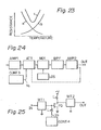
- the temperature characteristic of the resistance of each of the series connection of the PTC resistors and the NTC resistors shows, as illustrated in Fig. 23, a V-shaped curve.
- the resistance-temperature characteristic of the NTC resistor is represented by a curve a
- the resistance-temperature characteristic of the PTC resistor is represented by a curve b
- the resistance--temperature characteristic of the series resistance is represented by the V-shaped curve c.
- the resistance-temeprature characteristics of the series connections of the PTC resistors P231 through P233 and the NTC resistors S231 through S233 are represented, for example, by curves A, B and C of Fig. 17 respectively and the temperatures at which the series resistances of these series connections become minimum are designated by t 1 , t2 and t 3 .
- the gain to the voltage adjusted by the adjustable resistor RV231 becomes maximum and the control voltage V at this temperature can be adjusted by the adjustable resistor RV231.
- the control voltage V can be adjusted by the adjustable resistors RV232 and RV233 respectively.
- the circuit of Fig. 22 outputs control voltages which continuously vary in accordance with the change of the ambient temperature.
- the characteristic of the control voltage can be adjusted at three predetermined degrees of temperature.
- Fig. 24 is a block circuit diagram illustrating a transmitter system which includes a control voltage generator according to the present invention.
- the transmitter system of Fig. 24 comprises an intermediate frequency amplifier AMP1, a voltage controlled attenuator ATT, a mixer MIX, a local oscillator LOS, a band pass filter BPF, a transmitter amplifier AMP2 and a temperature compensating voltage generator CONT3 such as the circuit of Fig. 7 or Fig. 10 in which the control voltage can be adjusted independently at every adjusting temperature.
- the conventional transmitter system used an automatic level control circuit (ALC) including a feedback loop as shown by the dotted line in Fig. 24 but did not contain the control voltage generator circuit CONT3.
- ALC automatic level control circuit
- the control voltage V is applied to the voltage controlled attenuator ATT from the control voltage generator circuit CONT3 in order to compensate the gain-temperature characteristic of the transmitter amplifier AMP2 and to obtain a constant transmitting level.
- the system according to the present invention it is possible to omit the feedback loop contained in the conventional system and, therefore, it is possible to make up a stable transmitter system.
- the transmitter system of Fig. 24 it is possible to use any one of the temperature compensating voltage generator circuits mentioned above.
- Fig. 25 is a block circuit diatram illustrating an amplifier circuit which includes a control voltage generator circuit CONT 4 according to the present invention in order to stabilize the gain thereof.
- the circuit of Fig. 25 comprises impedance matching circuits MT1 and MT2 disposed on the sides of the input terminal IN and the output terminal OUT, a field effect transistor FQ, the control voltage generator circuit CONT4 and two inductors L 1 and L 2 .
- the control voltage V G is supplied to the gate electrode of the field effect transistor FQ as a DC bias voltage from the control voltage generator circuit CONT4.
- The-control voltage generator circuit CONT4 generates the bias voltage which compensates for the gain-temperature characteristic of the field effect transistor FQ so that the gain of the amplifier circuit does not change even when the ambient temperature has changed.
- the amplifier * circuit of Fig. 25 it is possible to use any one of the temperature compensating voltage generator circuits mentioned above.
- Fig. 26 is a circuit diagram illustrating a local oscillator which is used in a microwave multiplex wireless communication system and whose oscillation frequency is stabilized by the control voltage generator circuit according to the present invention, for example, the control voltage generator circuit of Fig. 7.
- the oscillator of Fig. 26 comprises an amplifier section 281, a dielectric resonator 282, a hybrid circuit 283, a temperature compensating voltage generator circuit CONT5 and a decoupling capacitor C285.
- the amplifier section 281 comprises a field effect transistor 285, strip lines for impedance matching M281 through M285, resistors R281 through R283, capacitors C281 through C284 and inductors L281 and L282.
- the hybrid circuit 283 comprises strip lines M286 and M287 each of which has.
- the hybrid circuit 283 distributes an output signal from the amplifier section 281 to the dielectric resonator 282 and an output terminal p out . It is possible to use any one of the temperature compensating voltage generator circuits mentioned above.
- the quantity of the phase shift from the input to the output of the amplifier section 281 which uses the field effect transistor 285 can be changed by changing the control voltage V G which is a gate bias voltage of the field effect transistor 285, so that the oscillation frequency can be finely changed. Therefore, the temperature characteristic of the oscillation frequency can be compensated by appropriately selecting parameters of the temperature compensating voltage generator circuit CONT5.
- the temperature conpensating voltage generator circuit CONTS an experiment was done by using a local oscillator whose oscillation frequency was 6 GHz and whose output signal level was +10 dBm. In this experiment, the frequency stability of the local oscillator was improved from +3 x 10 to + 1 x 10 -5 .
- the characteristic of the temperature compensating voltage can be adjusted independently at every adjusting temperature and the temperature compensating voltage varies continuously according to the change of the ambient temperature. Therefore, the temperature compensation of the characteristics of the electric circuits such as an oscillator, an amplifier, a voltage regulator, a transmitter and a receiver and so on can be effected almost completely. Moreover, according to the present invention, the characteristic of the control voltage can be readjusted without stopping the operation of the electric circuit by using the adjustable resistor corresponding to the ambient temperature, even if the characteristics of the electrical circuit has changed due to the secular variation.
Landscapes
- Engineering & Computer Science (AREA)
- Physics & Mathematics (AREA)
- Electromagnetism (AREA)
- General Physics & Mathematics (AREA)
- Radar, Positioning & Navigation (AREA)
- Automation & Control Theory (AREA)
- Power Engineering (AREA)
- Amplifiers (AREA)
- Oscillators With Electromechanical Resonators (AREA)
Abstract
Description
- The present invention relates to a temperature compensating voltage generator circuit, and more particularly to a temperature compensating voltage generator circuit used for temperature compensation of electric circuits whose electric characteristics can be controlled by a control voltage.
- In general, the electric characteristic of an electric circuit such as a gain or an oscillation frequency of an amplifier or an oscillator changes due to the change of the temperature of the surroundings and, therefore, such an electric circuit comprises a means for temperature compensation. For example, as illustrated in Fig. 1, a control voltage such as a DC bias potential of an electric circuit CKT, such as an amplifier which is operated by an operating voltage VCC , is produced by a control voltage generator circuit, 'i.e., temperature compensating voltage generator circuit consisting of resistors Rl and R2 and a negative coefficient temperature sensitive resistor S, and, the control voltage is changed in accordance with the change of the ambient temperature so that the electric characteristic such as the gain of the electric circuit CKT is maintained in a constant ocndition.
- Since the theoretical estimation of the temperature characteristics of the electric circuit CKT is generally difficult, the temperature characteristics are practically measured by using the practical circuit device and the resistors Rl and R2 and the negative temperature coefficient temperature sensitive resistor S are selected. However, in many cases the temperature characteristics of the electrical circuit CKT do not show simple or linear curves, so that the conventional means cannot effect the substantially complete temperature compensation and it takes a long time to determine the characteristic of the temperature compensating voltage generator circuit. When the characteristics of the electrical circuit CKT has changed due to the secular variation, it is necessary to stop the operation of the electric circuit CKT in order to readjust the characteristic of the temperature compensating voltage generator circuit.
- When it is necessary to effect complete temperature compensation, the characteristic of the electric circuit is practically measured at various temperatures and the control voltages, i.e., the temperature compensating voltages at the measured temperatures are determined so that the characteristic of the electric circuit is equalized. However, in the conventional temperature compensating voltage generator, it is impossible to adjust the value of the control voltage independently at various temperatures, so that the adjustment of the compensating voltage of the temperature compensating voltage generator circuit is very difficult. For example, when the compensating voltage is adjusted at another temperature after an adjustment of the compensating voltage at a base temperature, for example a normal temperature, the compensating voltage at the base temperature which is previously adjusted, changes.
- Moreover, in the above-mentioned conventional circuit, when the temperature characteristic of the control voltage for effecting temperature compensation cannot be approximated by a first order curve, it is very difficult to effect temperature compensation.
- It is the principal object of the present invention to provide.a temperature compensating voltage generator circuit in which the compensating voltage such as a DC bias voltage can be adjusted independently at each temperature in order to obtain a required characteristic of the compensating voltage.
- According to the present invention, there is provided a temperature compensating voltage generator circuit for compensating temperature characteristics of an electric circuit whose electrical characteristic can be controlled by a control voltage, which comprises:
- a plurality of voltage dividers each of which comprises a resistor circuit and a temperature sensitive circuit;
- a plurality of differential amplifiers each of which receives an output voltage from one of said voltage dividers;
- a plurality of level adjusting circuits for adjusting levels of output voltages from said differential amplifiers; and
- a combining circuit which combines output voltages from said level adjusting circuits in order to generate a temperature compensating voltage.
-
- Fig. 1 is a block circuit diagram illustrating an electric circuit comprising a conventional temperature compensating circuit;
- Fig. 2 is a circuit diagram illustrating the principle of the present invention;
- Fig. 3 is a graph illustrating an electrical characteristic of the circuit of Fig. 2;
- Fig. 4 is a circuit diagram illustrating a temperature compensating voltage generator circuit as an embodiment of the present invention;
- Fig. 5 is a graph illustrating a characteristic of the circuit of Fig. 4;
- Fig. 6 is a circuit diagram illustrating a temperature sensitive circuit as another embodiment of the present invention;
- Fig. 7 is a circuit diagram illustrating a temperature compensating voltage generator circuit as still another embodiment of the present invention;
- Fig. 8 is a circuit diagram illustrating a temperature compensating voltage generator circuit as still another embodiment of the present invention;
- Fig. 9 is a circuit diagram illustrating a quartz oscillator circuit having a temperature compensating voltage generator according to the present invention;
- Fig. 10 is a circuit diagram illustrating a temperature compensating voltage generator circuit as still another embodiment of the present invention;
- Fig. 11 is a graph illustrating an adjustable range of the temperature compensating voltage of the circuit of Fig. 10;
- Fig. 12 is a circuit diagram illustrating a temperature compensating voltage generator circuit as still another embodiment of the present invention;
- Fig. 13 is a circuit diagram illustrating a temperature compensating voltage generator circuit as still another embodiment of the present invention;
- Fig. 14 is a graph illustrating the characteristics of the temperature sensitive circuits included in the circuit of Fig. 13;
- Fig. 15 is a graph illustrating the temperature characteristic of the temperature compensating voltage of the circuit of Fig. 13;
- Fig. 16 is a circuit diagram illustrating a temperature compensating voltage generaotr circuit as still another embodiment of the present invention;
- Fig. 17 is a graph illustrating the characteristic of the temperature sensitive circuits included in the circuit of Fig. 16;
- Fig. 18 is a graph illustrating the characteristic of the input voltage of the differential amplifiers of Fig. 16;
- Fig. 19 is a circuit diagram illustrating a temperature compensating voltage generator circuit as still another embodiment of the present invention;'
- Fig. 20 is a circuit diagram illustrating a voltage regulator circuit having a temperature compensating voltage generator circuit according to the present invention;
- Fig. 21 is a circuit diagram illustrating a temperature compensating voltage generator circuit as still another embodiment of the present invention;
- Fig. 22 is a circuit diagram illustrating a temperature compensating voltage generator circuit as still another embodiment of the present invention;
- Fig. 23 is a praph illustrating a resistance-temperature characteristic of a temperature sensitive circuit of the circuit of Fig. 22;
- Fig. 24 is a block.circuit diagram illustrating a transmitter system having a temperature compensating voltage generator circuit according to the present invention;
- Fig. 25 is a block circuit diagram illustrating an amplifier circuit having a temperature compensating voltage generator circuit according to the present invention; and;
- Fig. 26 is a circuit diagram illustrating a microwave local oscillator having a temperature compensating voltage generator circuit according to the present invention.
- With reference to the attached drawings, the present invention will now be explained.
- Fig. 2 is a circuit, diagram which illustrates the principle of the present invention. In Fig. 2, a diode D and a resistor R are connected parallel with each other and a current i flows through this parallel circuit. When the voltage drop V of the parallel circuit is lower than the forward biased voltage VD of the diode D, the diode D is in a cut off condition so that the voltage drop V is equal to i·R and the voltage drop V can be changed by changing the resistance of the resistor R. When the voltage drop V reaches the forward biased voltage VD , for example about 0.7 V in the case of a silicone diode, the diode D turns on and a part of the current i flows through the diode D. In this condition, the voltage drop does not change and is equal to the forward biased voltage VD even if the value of the resistance of the resistor R is changed.
- Fig. 3 illustrates a relation between the voltage drop V of the aforementioned parallel circuit and the resistance of the resistor R. As apparent from Fig. 3, the voltage drop V is equal to the forward biased voltage VD when the resistance of the resistor R is equal to or larger than R'. Where R' is equal to VD/i. Assume that the forward biased voltage VD is equal to 0.7 V and the current i is equal to 2mA. In this condition, when the resistance of the resistor R is equal to or larger than 350 ohms. The voltage drop V is equal to 0.7 V, and, when the resistance of the resistor R is lower than 350 ohm, the voltage drop V is equal to the product of the resistance value of the resistor R and the current value i.
- In the present invention, the resistor R is substituted by a negative or positive temperature coefficient temperature sensitive resistor. Therefore, in a range of the ambient temperature in which the resistance of the temperature sensitive resistor is lower than R' of Fig. 3, the voltage drop V changes in accordance with the change of the ambient temperrature. In a range of the ambient temperature in which the resistance of the temperature sensitive resistor is higher than or equal to R', the voltage drop V is approximately equal to the forward biased voltage VD and does not change even when the ambient temperature has changed.
- Fig. 4 is a circuit diagram illustrating a temperature compensating voltage generator circuit as an embodiment of the present invention. The circuit of Fig. 4 comprises adjustable resistors R41 through R46, positive temperature coefficient temperature sensitive resistors(hereinafter referred to as PTC resistors) P41 and P42, negative temperature coefficient temperature sensitive resistors (hereinafter referred to as NTC resistors) S41 and S42 and diodes D41 through D44. In Fig. 4, V designates the potential of a voltage source and V designates the potential of the control voltage, i.e., the temperature compensating voltage. The diode D41, the PTC resistors P41 and the resistor R42 constitute a first temperature sensitive circuit, the diode D42, the NTC resistors S41 and the resistor R43 constitute a second temperature sensitive circuit, the diode D43, the PTC resistor P42 and the resistor R44 constitute a third temperature sensitive circuit, and, the diode D44, the NTC resistor S42 and the resistor R45 constitute a fourth temperature sensitive circuit. Assume that each of the PTC resistors P41 and P42 and the NTC resistors S41 and S42 of the first through the fourth temperature circuits has a larger resistance than R' of Fig. 3 at the base temperature, for example the normal temperature. In this condition,'the diodes D41 through D44 are all in a turned on condition regardless of the resistance value of the resistors R42 through R45 and the control voltage VG can be adjusted by changing the resistance of the resistors R41 and R46. The control voltage V is as follows.
-

- When the ambient temperature is lower than the base temperature, the resistances of the PTC resistors P41 and P42 decrease and the resistances of the NTC resistors S41 and S42 increase. Therefore, at such a lower temperature, if the resistance of the resistor R42 is adjusted so as to turn off the diode D41, a current from the voltage source flows through the PTC resistor P41 and the resistor R42. Therefore, the potential drop of the first temperature sensitive circuit becomes smaller than the forward biased voltage VD of the diode D41 and determined by the total resistance of the series connection of the PTC resistor P41 and the resistor R42. In this condition, the control voltage VG becomes higher than that of the base temperature. At such a lower temperature, if the resistance of the resistor R44 of the third temperature sensitive circuit is adjusted so as to turn off the diode D43, the control voltage VG becomes lower than that of the base temperature. It should be noted that, at such a lower temperature, the resistances of the NTC resistors S41 and S42 become larger and thus the voltage drop of each of the second and fourth temperature sensitive circuits is equal to the forward biased voltage VD.
- When the ambient temperature is higher than the base temperature, the control voltage VG can be higher or lower than that of the base temperature by adjusting the resistance of the resistor R43 or R45 of the second or fourth temperature sensitive circuit so as to turn off one of the diodes D42 and D44. The resistance-temperature characteristics of the PTC resistors P41 and P42 or of the NTC resistors S41 and S42 can be equal to each other or can be different from each other. If the PTC resistors P41 and P42 and/or the NTC resistors S41 and S42 having the different resistance-temperature characteristics are used, it is also possible to generate the control voltage V determined by the difference of the resistance-temperature characteristics in the condition the diodes D41 and D43 and/or-the diodes D42 and D44 are both turned on at the same temperature.
- Fig. 5 illustrates an adjustable range of the control voltage V of the circuit in Fig. 4. After the control voltage V at the base temperature T is adjusted to be VG1 by using the resistors R41 and R46, the level of the control voltage at a lower temperature Tl can be adjusted by the resistor R42 or R44' and the level of the control voltage at a higher temperature Th can be ajusted by the resistor R43 or R45 within the hatched range of Fig. 5. It should be noted that the level of the control voltage VG1 at the base temperature T is not changed even when the levels of the control voltage at the lower temperature Tl and the higher temperature Th are changed. Therefore, it is possible to independently adjust the level of the control voltage at each adjusting temperature. The control voltage changes continuously according to the change of the ambient temperature within a range including the adjusting temperatures such as the high temperature Th and the lower temperature Tl.
- In the hatched adjustable range of Fig. 5, an area A is obtained by the resistance value of the resistor R42 and the resistor-temperature characteristic of the PTC resistor P41 of the first temperature sensitive circuit, and areas B, C and D are obtained by the second, third and fourth temperature sensitive circuits, respectively.
- In Fig. 5, if the control voltage VG at the base temperature T is adjusted to VG2, the adjustable range of the control voltage VG becomes an area shown by dotted lines of Fig. 5.
- In each of the first through the fourth temperature sensitive circuits mentioned above, each includes one diode which can be D41, D42, D43 or D44, the maximum adjustable range of the voltage drop is the forward biased voltage V of each of the diodes D41 through D44. However, as illustrated in Fig. 6, the maximum adjustable range of each of the temperature sensitive circuits can be expanded by using a series connection of a plurality of diodes such as D , Db and DC which is connected parallel to a series connection of the resistor R and the PTC resistor P or the NTC resistor S. When the series connection of three diodes Da, Db and D each having the forward biased voltage VD of 0.7 V is used, the voltage drop of each temperature sensitive circuit can be changed in a range from 0 through 2.1 V. Practically speaking, the voltage drop of the temperature sensitive circuit of Fig. 6 does not become zero even if the resistance of the resistor R is adjusted to zero, since the resistance of the PTC resistor P or the NTC resistor S does not become zero.
- . Fig. 7 illustrates another embodiment of the present invention. The temperature compensating voltage generator of Fig. 7 comprises adjustable resistors R70 through R73, diodes D71 and D72, PTC resistors P71 and P72 and NTC resistors S71 and S72. The control voltage VG at the base temperature is obtained by dividing a voltage -V by the resistors R70 and R73. The resistance-temperature characteristics are selected so that the resistance of each of the PTC resistors P71 and P72 and the NTC resistors S71 and S72 is large and the diodes D71 and D72 are turned on. Therefore, at the base temperature, a current flows through the resistor R73, the diodes.D72 and D71 and the resistor R70, and the control voltage V does not change even if the resistances of the resistor R71 and R72 are changed.
- The adjustment of the temperature characteristic of the circuit of Fig. 7 in a higher or lower temperature is effected by the resistors R71 and R72. For example, if the sliders of the resistors R71 and R72 are both moved to the direction of the NTC resistor S71 and the PTC resistor P71, the diode D72 is in a turned on condition both at the lower temperature and at the higher temperature and the diode D71 is in a turned off condition. Since at the lower temperature, the resistance of the PTC resistor P71 becomes low due to its resistor-temperature characteristic and at the higher temperature, the resistance of the NTC resistor S71 becomes low due to its resistor-temperature characteristic, the control voltage VG of both the higher (and lower temperature becomes higher) than that of the base temperature.
- If the sliders of the resistors R71 and R72 are both moved in the direction of the NTC resistor S72 and the PTC resistor P72, the diode D72 is in a turned off condition both at the lower temperature and at the higher temperature. Therefore, the control voltage V of both the higher and lower temperature becomes lower than that of the base temperature.
- Fig. 8 illustrates a temperature compensating voltage generator circuit as still another embodiment of the present invention. In the above-mentioned embodiment, the characteristic of the control voltage VG can be adjusted at three points, i.e., the base temperature, the lower temperature and the higher temperature. While in this embodiment of Fig. 8, the characteristic of the control voltage V can be adjusted at five points. The circuit of Fig. 8 comprises a first through an eighth temperature sensitive circuit which comprise diodes D81 through D88, resistors R81 through R88, and, PTC resistors P81 through P84 and NTC resistors S81 through S84. At the base temperature, the control voltage V is adjusted by changing the resistances of resistors R80 and R89 which divides a power supply voltage -V. The PTC resistors P81 and P82 of the first and the third temperature sensitive circuits have different resistor-temperature characteristics and the NTC resistors S81 and S82 of the second and the fourth temperature sensitive circuits have different resistor-temperature characteristics. The PTC resistors P83 and P84 of the fifth and the seventh temperature sensitive circuits and the NTC resistors S83 and S84 of the sixth and the eighth temperature sensitive circuits have also different resistor-temperature characteristics. Therefore, the adjustable points of the temperature can be increased.
- 'For example, the resistor-temperature characteristics of the NTC resistors and the PTC resistors of the first through the eighth temperature sensitive circuits are selected so as to turn on all the diodes D81 through D88 at the base temperature. The control voltage V is adjusted to a value by setting the resistances of the resistors R80 and R89 at the base temperature. At a first low temperature which is lower than the base temperature, the resistances of the resistors R83 and R87 of the third and the seventh temperature sensitive circuits are adjusted. The PTC resistors P81 and P83 of the first and the fifth temperature sensitive circuits are selected so that the diodes D81 and D85 are not turned off at the first low temperature and the diodes D81 and D85 are turned off at a second low temperature which is lower than the first temperature if the resistances of the resistors R81 and R85 are decreased, for example, to zero. Therefore, at the second low temperature, the control voltage VG can be adjusted by the resistors R81 and R85 of the first and the fifth temperature sensitive circuits.
- At a first high temperature which is higher than the base temperature, the control voltages VG can be adjusted by the resistors R84 and R88 of the fourth and the eighth temperature sensitive circuits and, at a second high temperature which is higher than the first high temperature, the control voltage VG can be adjusted by the resistors R82 and R86 of the second and the sixth temperature sensitive circuits. The NTC resistors S81 and S83 are selected so that the resistances thereof are large so as to keep the diodes D82 and D86 in a turned on condition at the first high temperature and the resistances thereof become small so as to keep the diodes D82 and D86 in a turned off condition at the second high temperature.
- Therefore, in the circuit of Fig. 8, it is possible to set the control voltages at every temperature independently by adjusting the resistors of the respective temperature sensitive circuits after the adjustment of the control voltage at the base temperature.
- In the above-mentioned embodiments, it is possible to replace the diodes of the temperature sensitive circuits by zener diodes. It is also possible to connect a direct current amplifier to the output terminal of the temperature compensating voltage generator circuit in order to enlarge the variable range of the output control voltage VG. It is further possible to constitute all temperature sensitive circuits by using only the PTC resistors or only the NTC resistors as the temperature sensitive resistors, if the temperature characteristic of the electric circuit is limited.
- Fig. 9 illustrates an oscillator circuit whose frequency-temperature characteristic is compensated by using the aforementioned temperature compensating voltage generator circuit of Fig. 7. The oscillator circuit of Fig. 9 comprises a control
voltage generator CONT 1, an oscillator portion CKT1 and a decoupling circuit consisting of a zener diode ZD, a capacitor C5 and a resistor R95. The oscillator portion CKT1 comprises a quartz oscillator element XTL, a transistor Q, a variable capacitance diode CD, inductors L1 and L2 capacitors Cl through C4 and resistors R91 through R94. The control voltage generator CONT1 has the same circuit structure as the circuit of Fig. 7 and comprises variable or adjustable resistors RV91 through RV94, diodes D91 and D92, NTC resistors S91 and S92 and PTC resistors P91 and P92. - In the oscillator portion CKT1, the oscillation frequency can be changed by the potential applied to the variable capacitor diode CD, and the potential is supplied from the control
voltage generator CONT 1. - In the circuit of Fig: 9, the resistance-temperature characteristics of the NTC resistors S91 and S92 and the PTC resistors P91 and P92 are selected so that the resistance of each of these NTC resistors and the PTC resistors is large and thus a current flows through the diodes D91 and D92 and the resistors RV91 and RV94 at the base temperature for example the normal temperature of 25°C. Assume that the forward biased voltage of the diodes D91 and D92 is V and the potential of the power supply voltage applied to the control
voltage generator CONT 1 is V. In this condition, the control voltage V is as follows.
- If the
oscillator portion CKT 1 has a frequency--temperature characteristic that the oscillation frequency at a high temperature which is, for example, 20°C higher than the base temperature becomes lower than that of the base temperature and the oscillation frequency at a low temperature which is, for example, 20°C lower than the base temperature also becomes lower than that of the base temperature, it is necessary to raise the oscillation frequencies at the high and the low temperature. For this purpose, the sliders of the adjustable resistors RV92 and RV93 are both adjusted to positions which are nearer to the NTC resistor S91 and the PTC resistor P91 respectively. Therefore, at the high temperature, the resistance of the NTC resistor S91 becomes low and the diode D91 is turned off, so that the control voltage VG becomes large in accordance with the decrease of the resistance of the NTC resistor S91. The temperature characteristic of the control voltage can be adjusted by the adjustable resistor RV92. - At the low temperature, the resistance of the PTC resistor P91 becomes low and the diode D91 is turned off, so that the control voltage VG becomes high in accordance with the decrease of the resistance of the PTC resistor P91. The amount of the change of the control voltage in accordance with the change of the temperature can be adjusted by the adjustable resistor RV93.
- Contrary to the above-mentioned case, if it is necessary to lower the control voltage both at the high and the low temperature, the sliders of the adjustable resistors RV92 and RV93 are moved to positions which are nearer to the NTC resistor S92 and the PTC resistor P92 respectively.
- Therefore, in the above-mentioned circuit of Fig. 9, the control voltages at the high and the low temperature can be independently adjusted by the adjustable resistors RV92 and RV93 after the adjustment of the control voltage at the base temperature, and thus the adjustment of the control voltage V can be easily adjusted and the frequency--temperature characteristic of the oscillator circuit can be completely compensated.
- Practical experiments showed that the stability of the oscillation frequency was improved from +10 x 10-6 to +2 x 10⁶ at the temperature range of 0 through 50°C. In this case, the adjustment of the control voltage V was first effected at the base temperature of 25°C and then at the high temperature of 50°C and the low temperature of 0°C.
- Fig. 10 is a circuit diagram illustrating another embodiment of the present invention. The temperature compensating voltage generator circuit of Fig. 10 comprises resistors R101 through R108, negative coefficient temperature sensitive resistor, i.e., a NTC resistor S101, a positive coefficient temperature sensitive resistor, i.e., a PTC resistor P101, diodes D101 and D102, differential amplifiers DFAl and DFA2, adjustable resistors RV101 through RV103 and an operational amplifier OPA. OUT designates an output terminal of the control voltage and +V and -V designate power supply voltages. To a non-inverted input terminal of the operational amplifier OPA, a constant voltage from the voltage divider circuit consisting of the resistors R107 and R108 is applied and to an inverted input terminal of the operational amplifier OPA, voltages adjusted by the adjustable resistors RV101 through RV103 are applied through the resistors R103 through R105 respectively, so that the addition circuit is constituted. Output voltages from a voltage divider circuit consisting of the resistor R101 and the NTC resistor S101 and from another voltage divider circuit consisting of the resistor R102 and the PTC resistor P101 are respectively applied to the input terminals of the differential amplifier DFAl and DFA2 through the diodes D101 and D102, and the output voltages. from the differential amplifiers DFA1 and DFA2 are applied to the adjustable resistors RV101 and RV103 respectively.
- Assume that, at the base temperature for example the normal temperature, the resistances of the NTC resistor S101 and the resistor R101 are equal to each other and the resistances of the PTC resistor P101 and the resistor R102 are equal to each other. In this condition, the potentials of a point a and a point b in Fig. 10 are both equal to zero and the diodes D101 and D102 are both in a cut off condition so that the output potentials of the differential amplifiers DFAl and DFA2 are both equal to zero. As a result, the control voltage VG from the output terminal OUT of the operational amplifier OPA is proportional to the output voltage from the adjustable resistor RV102. Therefore, at the base temperature, the control voltage V can be adjusted by the adjustable resistor RV102.
- At a high temperature which is higher than the base temperature, the resistance of the NTC resistor S101 becomes smaller and the potential of the point a of Fig. 10 becomes negative, so that the diode D101 is turned on and the differential amplifier DFAl outputs a potential voltage corresponding to the potential of the point a. The output potential of the differential amplifier DFAl is divided by the adjustable resistor RV101 and supplied to the inverted input terminal of the operational amplifier OPA through the resistor R103 to which the potential adjusted by the adjustable resistor RV102 is supplied through the resistor R104. Therefore, at a high temperature, the control voltage VG can be adjusted by the adjustable resistor RV101. It should be noted that, at a high temperature, the resistance of the PTC resistor P101 becomes larger and the potential of the point b of Fig. 10 becomes positive so that the diode D102 is turned off and the output potential of the differential amplifier DFA2 is maintained at zero.
- At a low temperature which is lower than the base temperature, the resistance of the NTC resistor S101 becomes larger and the potential of the point a of Fig. 1 becomes positive so that the diode D101 is turned off and the output potential of the differential amplifier DFA1 becomes zero. The resistance of the PTC resistor P101 becomes smaller and the potential of the point b of Fig. 10 becomes negative so that the diode D102 is turned on and the differential amplifier DFA2 outputs a potential voltage corresponding to the potential of the point b of Fig. 10. The output potential from the differential amplifier DFA2 is divided by the adjustable resistor RV103 and added to the potential adjusted by the adjustable resistor RV102. Therefore, at a low temperature, the control voltage V can be adjusted by the adjustable resistor RV103.
- Fig. 11 illustrates adjustable ranges of the control voltage generated by the circuit of Fig. 10. In Fig. 11, if the control voltage is adjusted to VG1 at the base temperature Tb , the adjustable range of the control voltage VG in a temperature range including the low temperature Ta and the high temperature tb becomes an area between the solid lines of Fig. 11. If the control voltage V at the base temperature Tb is adjusted to VG2 , the adjustable range of the control voltage VG in the same temperature range becomes the area between the dotted lines of Fig. 11. It should be noted that at-every adjusting point such as t , tb and t , the control voltage VG can be adjusted independently.
- Fig. 12 is a circuit diagram illustrating a temperature compensating voltage generator as another embodiment of the present invention. The circuit of Fig. 12 corresponds to a circuit in which the PTC resistor P101 and the resistor R102 of Fig. 10 are respectively replaced by a resistor R122 and a NTC resistor S122. It is also possible to use the NTC resistors S121 and S122 having the same resistor-temperature characteristic with each other. In this embodiment, the potentials of the point a and the point b varies in accordance with the change of the ambient temperature. Therefore, after the adjustment of the control voltage by the adjustable resistor RV102 at the base temperature, the control voltages at a high temperature and at a low temperature can be independently adjusted by the adjustable resistors RV101 and RV103 respectively.
- In the circuit of Fig. 12, it is also possible to use PTC resistors instead of the NTC resistors S121 and S122. In such a case, the control voltage at the high temperature can be adjusted by the adjustable resistor RV103 and the control voltage at the low temperature can be adjusted by the adjustable resistor RV101, independently. It is also possible to replace the adjustable resistor RV102 used for the adjustment of the control voltages at the base temperature by a voltage divider circuit having a fixed division ratio and to connect a voltage divider circuit comprising an adjustable resistor to the non-inverted input terminal of the operational amplifier OPA, so that the control voltage at the base temperature can be adjusted by the adjustable resistor. It is also possible to invert the polarity of connection of the diodes D101 and D102. In such a case the adjustable resistors corresponding to the high temperature and the low temperature are replaced by each other. It is also possible to omit the diodes D101 and D102 in case the resistance-temperature characteristics of the temperature sensitive resistors used in the control voltage generator circuit are differen6"from each other.
- Fig. 13 is a circuit diagram illustrating a temperature compensating voltage generator circuit as still another embodiment of the present-invention. In this embodiment, the adjustment of the characteristic of the control voltage can be effected at five points, i.e., the base temperature, a first and a second low temperature and a first and a second high temperature. The circuit of Fig. 13 comprises NTC resistors S131 and S132, PTC resistors P131 and P132, resistors R131 through R143, diodes D131 through D134 differential amplifiers DFAll through DFA14, adjustable or variable resistors RV131 through RV135 and an operational amplifier OPAl. OUT designates an output terminal of the control voltage and +V and -V designate power supply voltages. The resistance-temperature characteristics of the NTC resistors S131 and S132 are different from each other, or, if the resistance-temperature characteristics are the same, the resistance of the resistors R131 and R132 which are respectively connected to the NTC resistors S131 and S132 are different from each other. With regard to the PTC resistors P131 and P132, the resistance-temperature characteristics are different from each other, or, the resistance of the resistors R134 or R135 which are respectively connected to the PTC resistors P131 and P132 are different from each other. Therefore, the potentials of points a through d of Fig. 13 are different for every degree of the adjustable temperature. For example, these NTC resistors and PTC resistors are selected so that the differential output potentials Va through Vd from the differential amplifiers DFA11 through DFA14 become as illustrated in Fig. 14.
- At the base temperature, for example, t3 of Fig. 14, the control voltage can be adjusted by the adjustable resistor RV133. At the first high temperature t4 which is higher than the base temperature t3 and at the second high temperature which is higher than the first high temperature t4 , the control voltages can be adjusted by the adjustable resistors RV132 and RV131 respectively. At the first low temperature t2 which is lower than the base temperature and at the second low temperature tl which is lower than the first low temperature t2 , the control voltage'can be adjusted by the adjustable resistors RV134 and RV135, respectively.
- Fig. 15 illustrates an adjustable range of the control voltage. In the circuit of Fig. 13, since negative or positive voltage at each temperature t1, t2 , t4 and t5 is added to the control voltages at the base temperature t3, it is also possible, for example, to adjust the temperature characteristic of the control voltage so that the control voltage at the first high temperature t4 is higher than that at the base temperture t3 and the control voltage at the second high temperature t5 is lower than that at the base temperature.
- Fig. 16 is a circuit diagram illustrating a temperature compensating voltage generator circuit as still another embodiment of the present invention. The circuit of Fig. 16 comprises temperature sensitive circuits each comprising a series connection of a PTC resistor P161, P162, or P163 and a NTC resistor S161, S162 or S163 the circuit of Fig. 16 also comprises diodes D161 through D163, differential amplifiers DFA21 through DFA23, resistors R161 through R169, adjustable resistors RV161 through RV163 and an operational amplifier OPA2. OUT designates an output terminal of the control voltage and +V and -V designate power supply voltages. The resistance-temperature characteristic of each series connection in each of the temperature sensitive circuits have, as illustrated by A, B or C in Fig. 17, a valley point at which the total resistance of the series connection becomes minimum and the valley points in each temperature sensitive circuit differ from each other. The input voltages of the differential amplifiers DFA21 through DFA23 have temperature characteristics as illustrated by A', BI and C' of Fig. 18. Therefore, at the temperatures t1, t2 and t3 , the output potentials from the differential amplifiers DFA21, DFA22 and DFA23 respectively become maximum, and the characteristic of the control voltage can be adjusted independently by the adjustable resistors RV161, RV162 and RV163 at the temperatures t1, t2 and t3 respectively.
- Fig. 19 is a circuit diagram illustrating & temperature compensating voltage generator circuit as still another embodiment of the present invention. The circuit of Fig. 19 comprises adjustable or variable resistors RV191 through RV193 constituting voltage dividers whose voltage division ratios are adjustable, a NTC resistor S191, a PTC resistor P191, resistors R191 through R194 and an operational amplifier OPA191. In Fig. 19, OUT designates an output terminal of the control voltage and +VCC designates a power supply voltage. In the circuit of Fig. 19, a constant voltage from a voltage divider circuit which consists of the resistors R192 and R193 and which divides the power supply voltage +VCC is applied to the non-inverted input terminal of the operational amplifier OPA191. The inverted input terminal of the operational amplifier OPA191 receives the voltages adjusted by the adjustable resistors RV191, RV192 and RV193 through the NTC resistor S191, the resistor R191 and the PTC resistor p191 repectively, that is, the adjusted voltages are added by the adder circuit which comprises the NTC resistor S191, the resistor R191, the PTC resistor p191, the feedback resistor R194 and the operational amplifier OPA191 and which adds the adjusted voltages under the gains corresponding to the ratio of the resistance of the NTC resistor S191, the resistor R191 and the PTC resistor P191 to the feedback resistor R194.
- At the base temperature, the resistance of the NTC resistor S191 and the PTC resistor P191 is larger than that of the resistor R191, and thus the gain of the voltage adjusted by the adjustable resistor RV192 is larger than that of each of the voltages from the adjustable resistors RV191 and RV193. Therefore, at the base temperature, the control voltage VG can be adjusted by the adjustable resistor RV192.
- At a low temperature which is lower than the base temperature, the resistance of the PTC resistor pl91 becomes smaller so that the gain of the voltage adjusted by the adjustable resistor RV193 becomes large and, therefore, the control voltage V at the low temperature can be adjusted by the adjustable resistor R193.
- At a high temperature which is higher than the base temperature, the resistance of the NTC resistor S191 becomes smaller so that the gain of the voltage adjusted by the adjustable resistor RV191 becomes large and, therefore, the control voltage VG at the high temperature can be adjusted by the adjustable resistor R191.
- The adjustable range of the control voltage VG of the circuit of Fig. 19 is the same as the adjustable range illustrated in Fig. 11. As apparent from Fig. 11, if the control voltage is adjusted to VG1 at the base temperature tb, the adjustable range of the control voltage VG in the temperature range including the low temperature ta and the high temperature tc becomes the range illustrated by solid lines of Fig. 11. If the control voltage is adjusted to VG2 at the base temperature tb, the adjustable range becomes the range illustrated by the dotted lines.
- Fig. 20 illustrates a voltage regulator system comprising the control voltage generator circuit of Fig. 19. In Fig. 20, a voltage regulator circuit CKT2 receives an input voltage Vin and outputs a stabilized output voltage Vout. The regulating characteristic of the voltage regulator circuit CKT2 varies in accordance with the change of the ambient temperature and thus the potential of the output voltage Vout changes according to the variation of the ambient temperature. In order to gain the output voltage Vout having a constant potential, the control voltage, i.e., temperature compensating voltage VG is applied from the control voltage
generator circuit CON T2 to the voltage regulator circuit CKT2. The control voltage VG is, for example, added to the error voltage of the voltage regulator circuit CKT2 detected from the output voltage Vout and a reference voltage not shown in the drawing. - Fig. 21 is a circuit diagram illustrating a temperatur e compensating voltage generator circuit as still another embodiment of the present invention. In Fig. 21, the same parts as appear in Fig. 19 are designated by the same reference symbols. In Fig. 21, RV221 is an adjustable resistor and R221 and R222 are resistors. At the base temperature, the control voltage VG is adjusted by the adjustable resistor RV221, and the control voltage V is proportional to the difference between the adjusted voltage from the adjustable resistor RV221 and the voltage from the voltage divider circuit consisting of the resistors R221 and R222. At a low temperature, the resistance of the PTC resistor P191 becomes smaller and the voltage adjusted by the adjustable resistor RV193 is mainly added to the voltage at the base temperature. At a high temperature, the resistance of the NTC resistor S191 becomes smaller and the voltage adjusted by the adjustable resistor RV191 is mainly added to the voltage at the base temperature. Therefore, after the adjustment of the control voltage V by the adjustable resistor RV221, the control voltages at the low and the high temperatures can be adjusted independently by the adjustable resistors RV193 and RV191.
- Fig. 22 is a circuit diagram illustrating a tmeperature compensating voltage generator circuit as still another embodiment of the present invention. The circuit of Fig. 22 comprises PTC resistors P231 through P233 whose resistance--temperature characteristics are different from each other, NTC resistors S231 through S233 whose resistance-temperature characteristics are different from each other, an operational amplifier OPA, adjustable resistors RV231 through RV233 which constitute voltage divider circuits and resistors R231 through R233. The temperature characteristic of the resistance of each of the series connection of the PTC resistors and the NTC resistors shows, as illustrated in Fig. 23, a V-shaped curve. The resistance-temperature characteristic of the NTC resistor is represented by a curve a, the resistance-temperature characteristic of the PTC resistor is represented by a curve b and the resistance--temperature characteristic of the series resistance is represented by the V-shaped curve c.
- Assume the the resistance-temeprature characteristics of the series connections of the PTC resistors P231 through P233 and the NTC resistors S231 through S233 are represented, for example, by curves A, B and C of Fig. 17 respectively and the temperatures at which the series resistances of these series connections become minimum are designated by t1, t2 and t3. In this condition, at the lowest temperature t1, the gain to the voltage adjusted by the adjustable resistor RV231 becomes maximum and the control voltage V at this temperature can be adjusted by the adjustable resistor RV231. At the temperatures t2 and t3 , the control voltage V can be adjusted by the adjustable resistors RV232 and RV233 respectively. At the temperatures between the adjusting temperatures t1, t2 and t3 , the circuit of Fig. 22 outputs control voltages which continuously vary in accordance with the change of the ambient temperature.
- In the embodiment of Fig. 22, the characteristic of the control voltage can be adjusted at three predetermined degrees of temperature. However, it is possible to increase the number of the series connections of the NTC resistors and the PTC resistors and to increase the number of the adjusting points, in order to output the control voltage having a complex temperature characteristic. It is also possible to connect an amplifier to the output terminal OUT which converts an output impedance or which enlarges the variable range of the control voltage VG. It is also possible to connect a photo-coupler to the output terminal OUT in oder to electrically separate the output terminal OUT and the load circuits.
- Fig. 24 is a block circuit diagram illustrating a transmitter system which includes a control voltage generator according to the present invention. The transmitter system of Fig. 24 comprises an intermediate frequency amplifier AMP1, a voltage controlled attenuator ATT, a mixer MIX, a local oscillator LOS, a band pass filter BPF, a transmitter amplifier AMP2 and a temperature compensating voltage generator CONT3 such as the circuit of Fig. 7 or Fig. 10 in which the control voltage can be adjusted independently at every adjusting temperature. In order to maintain the output signal level at a constant value, the conventional transmitter system used an automatic level control circuit (ALC) including a feedback loop as shown by the dotted line in Fig. 24 but did not contain the control voltage generator circuit CONT3. In such a conventional transmitter system, it was necessary to adjust the loop gain precisely so that the self-oscillation of the system did not occur and thus the design, manufacturing and adjusting of the circuit was difficult. In the transmitter system according to the present invention, the control voltage V is applied to the voltage controlled attenuator ATT from the control voltage generator circuit CONT3 in order to compensate the gain-temperature characteristic of the transmitter amplifier AMP2 and to obtain a constant transmitting level. In the system according to the present invention, it is possible to omit the feedback loop contained in the conventional system and, therefore, it is possible to make up a stable transmitter system. In the transmitter system of Fig. 24, it is possible to use any one of the temperature compensating voltage generator circuits mentioned above.
- Fig. 25 is a block circuit diatram illustrating an amplifier circuit which includes a control voltage
generator circuit CONT 4 according to the present invention in order to stabilize the gain thereof. The circuit of Fig. 25 comprises impedance matching circuits MT1 and MT2 disposed on the sides of the input terminal IN and the output terminal OUT, a field effect transistor FQ, the control voltage generator circuit CONT4 and two inductors L1 and L2. The control voltage VG is supplied to the gate electrode of the field effect transistor FQ as a DC bias voltage from the control voltage generator circuit CONT4. The-control voltage generator circuit CONT4 generates the bias voltage which compensates for the gain-temperature characteristic of the field effect transistor FQ so that the gain of the amplifier circuit does not change even when the ambient temperature has changed. In the amplifier * circuit of Fig. 25, it is possible to use any one of the temperature compensating voltage generator circuits mentioned above. - Fig. 26 is a circuit diagram illustrating a local oscillator which is used in a microwave multiplex wireless communication system and whose oscillation frequency is stabilized by the control voltage generator circuit according to the present invention, for example, the control voltage generator circuit of Fig. 7. The oscillator of Fig. 26 comprises an
amplifier section 281, adielectric resonator 282, ahybrid circuit 283, a temperature compensating voltage generator circuit CONT5 and a decoupling capacitor C285. Theamplifier section 281 comprises afield effect transistor 285, strip lines for impedance matching M281 through M285, resistors R281 through R283, capacitors C281 through C284 and inductors L281 and L282. Thehybrid circuit 283 comprises strip lines M286 and M287 each of which has. a length that is a quarter of a wave length, and a resistor R284, and thehybrid circuit 283 distributes an output signal from theamplifier section 281 to thedielectric resonator 282 and an output terminal pout. It is possible to use any one of the temperature compensating voltage generator circuits mentioned above. - In the circuit of Fig. 26, the quantity of the phase shift from the input to the output of the
amplifier section 281 which uses thefield effect transistor 285 can be changed by changing the control voltage VG which is a gate bias voltage of thefield effect transistor 285, so that the oscillation frequency can be finely changed. Therefore, the temperature characteristic of the oscillation frequency can be compensated by appropriately selecting parameters of the temperature compensating voltage generator circuit CONT5. In order to confirm that the oscillation frequency can be stabilized by the temperature conpensating voltage generator circuit CONTS, an experiment was done by using a local oscillator whose oscillation frequency was 6 GHz and whose output signal level was +10 dBm. In this experiment, the frequency stability of the local oscillator was improved from +3 x 10 to +1 x 10⁻⁵. - As mentioned above, in the temperature compensating voltage generator circuit according to the present invention, the characteristic of the temperature compensating voltage can be adjusted independently at every adjusting temperature and the temperature compensating voltage varies continuously according to the change of the ambient temperature. Therefore, the temperature compensation of the characteristics of the electric circuits such as an oscillator, an amplifier, a voltage regulator, a transmitter and a receiver and so on can be effected almost completely. Moreover, according to the present invention, the characteristic of the control voltage can be readjusted without stopping the operation of the electric circuit by using the adjustable resistor corresponding to the ambient temperature, even if the characteristics of the electrical circuit has changed due to the secular variation.
Claims (9)
Applications Claiming Priority (8)
| Application Number | Priority Date | Filing Date | Title |
|---|---|---|---|
| JP56546/80 | 1980-04-28 | ||
| JP5654880A JPS56153972A (en) | 1980-04-28 | 1980-04-28 | Controlling voltage generating circuit |
| JP56548/80 | 1980-04-28 | ||
| JP56549/80 | 1980-04-28 | ||
| JP56547/80 | 1980-04-28 | ||
| JP5654780A JPS56153971A (en) | 1980-04-28 | 1980-04-28 | Controlling voltage generating circuit |
| JP5654980A JPS56153810A (en) | 1980-04-28 | 1980-04-28 | Electric circuit having temperature compensating function |
| JP5654680A JPS56153809A (en) | 1980-04-28 | 1980-04-28 | Control voltage generating circuit |
Related Parent Applications (1)
| Application Number | Title | Priority Date | Filing Date |
|---|---|---|---|
| EP81301812.4 Division | 1981-04-24 |
Publications (3)
| Publication Number | Publication Date |
|---|---|
| EP0108408A2 true EP0108408A2 (en) | 1984-05-16 |
| EP0108408A3 EP0108408A3 (en) | 1984-07-04 |
| EP0108408B1 EP0108408B1 (en) | 1987-07-01 |
Family
ID=27463364
Family Applications (3)
| Application Number | Title | Priority Date | Filing Date |
|---|---|---|---|
| EP81301812A Expired EP0039215B1 (en) | 1980-04-28 | 1981-04-24 | Temperature compensating voltage generator circuit |
| EP83111065A Expired EP0108408B1 (en) | 1980-04-28 | 1981-04-24 | Temperature compensating voltage generator circuit |
| EP83111066A Expired EP0108409B1 (en) | 1980-04-28 | 1981-04-24 | Temperature compensating voltage generator circuit |
Family Applications Before (1)
| Application Number | Title | Priority Date | Filing Date |
|---|---|---|---|
| EP81301812A Expired EP0039215B1 (en) | 1980-04-28 | 1981-04-24 | Temperature compensating voltage generator circuit |
Family Applications After (1)
| Application Number | Title | Priority Date | Filing Date |
|---|---|---|---|
| EP83111066A Expired EP0108409B1 (en) | 1980-04-28 | 1981-04-24 | Temperature compensating voltage generator circuit |
Country Status (3)
| Country | Link |
|---|---|
| US (1) | US4352053A (en) |
| EP (3) | EP0039215B1 (en) |
| DE (1) | DE3171674D1 (en) |
Cited By (6)
| Publication number | Priority date | Publication date | Assignee | Title |
|---|---|---|---|---|
| GB2233513A (en) * | 1989-06-09 | 1991-01-09 | Philips Electronic Associated | Oscillators |
| US5053692A (en) * | 1989-04-14 | 1991-10-01 | Lucas Industries P.L.C. | Temperature dependent power supply for use with a bridge transducer |
| EP0449567A2 (en) * | 1990-03-30 | 1991-10-02 | Texas Instruments Incorporated | Positive to negative voltage translator circuit and method of operation |
| FR2667742A1 (en) * | 1990-10-05 | 1992-04-10 | Cte Electro Piezo Electricite | TEMPERATURE COMPENSATED CRYSTAL OSCILLATOR. |
| EP0530072A1 (en) * | 1991-08-23 | 1993-03-03 | Thomson-Csf | Method and device for control and regulation |
| EP0913945A2 (en) * | 1997-10-31 | 1999-05-06 | CTS Corporation | Temperature compensating circuit for a crystal oscillator |
Families Citing this family (26)
| Publication number | Priority date | Publication date | Assignee | Title |
|---|---|---|---|---|
| US4463274A (en) * | 1982-02-01 | 1984-07-31 | Motorola, Inc. | Temperature compensation circuit for pressure sensor |
| US4587499A (en) * | 1982-06-07 | 1986-05-06 | Toyo Communication Equipment Co., Ltd. | Temperature compensating circuit for oscillator |
| JPS5939105A (en) * | 1982-08-27 | 1984-03-03 | Fujitsu Ltd | Temperature compensating circuit |
| US4478527A (en) * | 1982-12-02 | 1984-10-23 | General Signal Corporation | Temperature compensation for zero and span changes in a measurement circuit |
| US4562400A (en) * | 1983-08-30 | 1985-12-31 | Analog Devices, Incorporated | Temperature-compensated zener voltage reference |
| US4591743A (en) * | 1983-12-19 | 1986-05-27 | National Semiconductor Corporation | Temperature compensated current sensing circuit |
| US4883992A (en) * | 1988-09-06 | 1989-11-28 | Delco Electronics Corporation | Temperature compensated voltage generator |
| US4990846A (en) * | 1990-03-26 | 1991-02-05 | Delco Electronics Corporation | Temperature compensated voltage reference circuit |
| US5225716A (en) * | 1990-09-17 | 1993-07-06 | Fujitsu Limited | Semiconductor integrated circuit having means for suppressing a variation in a threshold level due to temperature variation |
| DE4216646C1 (en) * | 1992-05-20 | 1994-01-27 | Ant Nachrichtentech | Arrangement for providing an actuating signal for an attenuator |
| DE69412306T2 (en) * | 1993-01-25 | 1998-12-17 | Matsushita Electric Industrial Co., Ltd., Kadoma, Osaka | Temperature compensated quartz oscillator |
| JPH10164750A (en) * | 1996-11-26 | 1998-06-19 | Nec Corp | Output voltage varying system |
| US6437634B1 (en) | 1997-11-27 | 2002-08-20 | Nec Corporation | Semiconductor circuit in which distortion caused by change in ambient temperature is compensated |
| US6147557A (en) * | 1997-11-27 | 2000-11-14 | Nec Corporation | Semiconductor circuit compensating for changes in gain slope of the circuit's gain-frequency characteristic caused by ambient temperature changes |
| US6097240A (en) * | 1998-11-25 | 2000-08-01 | Antec Corporation | Temperature controlled attenuator and method for stabilizing a temperature-dependent voltage |
| FR2801116B1 (en) * | 1999-11-15 | 2002-01-25 | St Microelectronics Sa | CORRECTED VOLTAGE GENERATOR DEVICE AT LOW TEMPERATURE |
| US6356062B1 (en) * | 2000-09-27 | 2002-03-12 | Intel Corporation | Degenerative load temperature correction for charge pumps |
| US6917658B2 (en) * | 2002-09-16 | 2005-07-12 | Silicon Labs Cp, Inc. | Clock recovery method for bursty communications |
| US7395447B2 (en) * | 2002-09-16 | 2008-07-01 | Silicon Labs Cp, Inc. | Precision oscillator for an asynchronous transmission system |
| DE102004021441A1 (en) * | 2004-04-28 | 2005-12-01 | Siemens Ag | Method for compensating a temperature-induced frequency error of a quartz crystal |
| JP4990049B2 (en) * | 2007-07-02 | 2012-08-01 | 株式会社リコー | Temperature detection circuit |
| TW201003356A (en) * | 2008-07-10 | 2010-01-16 | Mobien Corp | Resistor device and circuit using the same |
| JP2014130099A (en) * | 2012-12-28 | 2014-07-10 | Toshiba Corp | Temperature detection circuit, temperature compensation circuit and buffer circuit |
| JP6468368B2 (en) * | 2015-12-07 | 2019-02-13 | 富士電機株式会社 | Voltage generation circuit and overcurrent detection circuit |
| US11831314B1 (en) * | 2022-08-31 | 2023-11-28 | Apple Inc. | Ratiometric current or voltage source circuit with reduced temperature dependence |
| TWI824794B (en) * | 2022-10-26 | 2023-12-01 | 新唐科技股份有限公司 | Calibration device and method for calibrating frequency drift and electronic device using the same |
Citations (1)
| Publication number | Priority date | Publication date | Assignee | Title |
|---|---|---|---|---|
| US3454903A (en) * | 1966-08-16 | 1969-07-08 | Int Standard Electric Corp | Temperature compensation of crystal oscillators |
Family Cites Families (10)
| Publication number | Priority date | Publication date | Assignee | Title |
|---|---|---|---|---|
| US3054966A (en) * | 1959-07-15 | 1962-09-18 | Gen Electric | Crystal controlled oscillator with temperature compensating means |
| US3278828A (en) * | 1962-05-28 | 1966-10-11 | Philips Corp | Rectifier circuit for use in wide range temperature environments |
| US3294974A (en) * | 1964-01-22 | 1966-12-27 | Mc Graw Edison Co | Photo-control device employing thermal relay |
| US3373379A (en) * | 1966-06-17 | 1968-03-12 | Motorola Inc | Crystal oscillator with temperature compensation |
| US3449599A (en) * | 1967-01-05 | 1969-06-10 | Atomic Energy Commission | Temperature control circuit |
| US3484867A (en) * | 1968-05-02 | 1969-12-16 | Atomic Energy Commission | Thermally stabilized class a or class b complementary transistor push-pull amplifier |
| NL6806969A (en) * | 1968-05-17 | 1969-05-27 | ||
| US3508168A (en) * | 1968-05-23 | 1970-04-21 | Hughes Aircraft Co | Crystal oscillator temperature compensating circuit |
| US4099415A (en) * | 1977-09-01 | 1978-07-11 | Systron-Donner Corporation | Temperature compensation circuit for a fluid damped servo system |
| US4243948A (en) * | 1979-05-08 | 1981-01-06 | Rca Corporation | Substantially temperature-independent trimming of current flows |
-
1981
- 1981-04-24 EP EP81301812A patent/EP0039215B1/en not_active Expired
- 1981-04-24 DE DE8181301812T patent/DE3171674D1/en not_active Expired
- 1981-04-24 EP EP83111065A patent/EP0108408B1/en not_active Expired
- 1981-04-24 EP EP83111066A patent/EP0108409B1/en not_active Expired
- 1981-04-27 US US06/257,551 patent/US4352053A/en not_active Expired - Fee Related
Patent Citations (1)
| Publication number | Priority date | Publication date | Assignee | Title |
|---|---|---|---|---|
| US3454903A (en) * | 1966-08-16 | 1969-07-08 | Int Standard Electric Corp | Temperature compensation of crystal oscillators |
Non-Patent Citations (3)
| Title |
|---|
| ELECTRONIC ENGINEERING, volume 51, no. 617, January 1979 (LONDON, GB) N. ALLEN-ROWLANDSON "Voltage reference has adjustable tempco", page 14 * |
| IBM TECHNICAL DISCLOSURE BULLETIN, volume 21, no. 8, January 1979 (NEW YORK, US) O.R. BUHLER et al. "Variable gain amplifiers", pages 3094-3096 * |
| REVUE DE PHYSIQUE APPLIQUEE, volume 12. no. 3, March 1977 (PARIS; FR) J.P. TROADEC et al. "Mesure simultanée d'une température", pages 503-509 * |
Cited By (10)
| Publication number | Priority date | Publication date | Assignee | Title |
|---|---|---|---|---|
| US5053692A (en) * | 1989-04-14 | 1991-10-01 | Lucas Industries P.L.C. | Temperature dependent power supply for use with a bridge transducer |
| GB2233513A (en) * | 1989-06-09 | 1991-01-09 | Philips Electronic Associated | Oscillators |
| EP0449567A2 (en) * | 1990-03-30 | 1991-10-02 | Texas Instruments Incorporated | Positive to negative voltage translator circuit and method of operation |
| EP0449567A3 (en) * | 1990-03-30 | 1992-02-26 | Texas Instruments Incorporated | Positive to negative voltage translator circuit and method of operation |
| FR2667742A1 (en) * | 1990-10-05 | 1992-04-10 | Cte Electro Piezo Electricite | TEMPERATURE COMPENSATED CRYSTAL OSCILLATOR. |
| WO1992006538A1 (en) * | 1990-10-05 | 1992-04-16 | Compagnie D'electronique Et De Piezo-Electricite C.E.P.E. | Temperature-compensated crystal oscillator |
| EP0530072A1 (en) * | 1991-08-23 | 1993-03-03 | Thomson-Csf | Method and device for control and regulation |
| US5341287A (en) * | 1991-08-23 | 1994-08-23 | Thomson-Csf | Method and apparatus for the control and regulation of a first magnitude of a device by action on a second magnitude |
| EP0913945A2 (en) * | 1997-10-31 | 1999-05-06 | CTS Corporation | Temperature compensating circuit for a crystal oscillator |
| EP0913945A3 (en) * | 1997-10-31 | 2000-03-22 | CTS Corporation | Temperature compensating circuit for a crystal oscillator |
Also Published As
| Publication number | Publication date |
|---|---|
| EP0039215B1 (en) | 1985-08-07 |
| EP0108409B1 (en) | 1987-03-25 |
| EP0108409A2 (en) | 1984-05-16 |
| US4352053A (en) | 1982-09-28 |
| EP0108408A3 (en) | 1984-07-04 |
| DE3171674D1 (en) | 1985-09-12 |
| EP0108409A3 (en) | 1984-07-04 |
| EP0108408B1 (en) | 1987-07-01 |
| EP0039215A1 (en) | 1981-11-04 |
Similar Documents
| Publication | Publication Date | Title |
|---|---|---|
| US4352053A (en) | Temperature compensating voltage generator circuit | |
| US5648718A (en) | Voltage regulator with load pole stabilization | |
| EP0248589B1 (en) | Temperature-compensated oscillator circuit | |
| US6294962B1 (en) | Circuit(s), architecture and method(s) for operating and/or tuning a ring oscillator | |
| EP0204088A2 (en) | Integrated circuit with a phase-locked loop | |
| US11398799B2 (en) | Offset drift compensation | |
| US11294410B2 (en) | Voltage regulator having a phase compensation circuit | |
| US4532468A (en) | Temperature-compensating voltage generator circuit | |
| US7535735B2 (en) | Compensation for parameter variations in a feedback circuit | |
| US5691671A (en) | Method and apparatus for a crystal oscillator using piecewise linear odd symmetry temperature compensation | |
| KR100609683B1 (en) | Temperature compensated Complementary Metal Oxide Semiconductor exponential function generator circuit | |
| PL127575B1 (en) | System of temperature compensation of gain of transistor amplifier | |
| US6879607B2 (en) | Semiconductor laser module | |
| JP3158000B2 (en) | Bias circuit | |
| US10833631B2 (en) | Amplifier bandwidth calibration of continuous time circuit | |
| US4668903A (en) | Apparatus and method for a temperature compensated reference voltage supply | |
| TW202238305A (en) | Shunt regulator | |
| US3443202A (en) | Temperature compensated transistorized power supply regulating means | |
| EP3101806B1 (en) | Variable gain amplifier circuit, controller of main amplifier and associated control method | |
| JP2002135051A (en) | Piezoelectric oscillator | |
| CN110531825B (en) | Amplifier circuit system, voltage regulating circuit and signal compensation method | |
| US7154325B2 (en) | Using active circuits to compensate for resistance variations in embedded poly resistors | |
| KR100794774B1 (en) | Temperature compensating circuit | |
| JPS6218926B2 (en) | ||
| JP2001196857A (en) | Crystal oscillator |
Legal Events
| Date | Code | Title | Description |
|---|---|---|---|
| PUAI | Public reference made under article 153(3) epc to a published international application that has entered the european phase |
Free format text: ORIGINAL CODE: 0009012 |
|
| PUAL | Search report despatched |
Free format text: ORIGINAL CODE: 0009013 |
|
| 17P | Request for examination filed |
Effective date: 19831117 |
|
| AC | Divisional application: reference to earlier application |
Ref document number: 39215 Country of ref document: EP |
|
| AK | Designated contracting states |
Designated state(s): DE FR GB IT |
|
| AK | Designated contracting states |
Designated state(s): DE FR GB IT |
|
| GRAA | (expected) grant |
Free format text: ORIGINAL CODE: 0009210 |
|
| AC | Divisional application: reference to earlier application |
Ref document number: 39215 Country of ref document: EP |
|
| AK | Designated contracting states |
Kind code of ref document: B1 Designated state(s): DE FR GB IT |
|
| ET | Fr: translation filed | ||
| REF | Corresponds to: |
Ref document number: 3176289 Country of ref document: DE Date of ref document: 19870806 |
|
| ITF | It: translation for a ep patent filed | ||
| PLBE | No opposition filed within time limit |
Free format text: ORIGINAL CODE: 0009261 |
|
| STAA | Information on the status of an ep patent application or granted ep patent |
Free format text: STATUS: NO OPPOSITION FILED WITHIN TIME LIMIT |
|
| 26N | No opposition filed | ||
| ITTA | It: last paid annual fee | ||
| PGFP | Annual fee paid to national office [announced via postgrant information from national office to epo] |
Ref country code: GB Payment date: 19920410 Year of fee payment: 12 |
|
| PGFP | Annual fee paid to national office [announced via postgrant information from national office to epo] |
Ref country code: FR Payment date: 19920429 Year of fee payment: 12 |
|
| PGFP | Annual fee paid to national office [announced via postgrant information from national office to epo] |
Ref country code: DE Payment date: 19920623 Year of fee payment: 12 |
|
| PG25 | Lapsed in a contracting state [announced via postgrant information from national office to epo] |
Ref country code: GB Effective date: 19930424 |
|
| GBPC | Gb: european patent ceased through non-payment of renewal fee |
Effective date: 19930424 |
|
| PG25 | Lapsed in a contracting state [announced via postgrant information from national office to epo] |
Ref country code: FR Effective date: 19931229 |
|
| PG25 | Lapsed in a contracting state [announced via postgrant information from national office to epo] |
Ref country code: DE Effective date: 19940101 |
|
| REG | Reference to a national code |
Ref country code: FR Ref legal event code: ST |