EP0108225B1 - Apparatus and method for transferring fault data from a recording device to a data processor - Google Patents
Apparatus and method for transferring fault data from a recording device to a data processor Download PDFInfo
- Publication number
- EP0108225B1 EP0108225B1 EP83109322A EP83109322A EP0108225B1 EP 0108225 B1 EP0108225 B1 EP 0108225B1 EP 83109322 A EP83109322 A EP 83109322A EP 83109322 A EP83109322 A EP 83109322A EP 0108225 B1 EP0108225 B1 EP 0108225B1
- Authority
- EP
- European Patent Office
- Prior art keywords
- signal
- fault
- peripheral device
- data
- adapter
- Prior art date
- Legal status (The legal status is an assumption and is not a legal conclusion. Google has not performed a legal analysis and makes no representation as to the accuracy of the status listed.)
- Expired
Links
Images

Classifications
-
- G—PHYSICS
- G06—COMPUTING; CALCULATING OR COUNTING
- G06F—ELECTRIC DIGITAL DATA PROCESSING
- G06F11/00—Error detection; Error correction; Monitoring
- G06F11/07—Responding to the occurrence of a fault, e.g. fault tolerance
- G06F11/0703—Error or fault processing not based on redundancy, i.e. by taking additional measures to deal with the error or fault not making use of redundancy in operation, in hardware, or in data representation
- G06F11/0766—Error or fault reporting or storing
- G06F11/0772—Means for error signaling, e.g. using interrupts, exception flags, dedicated error registers
-
- G—PHYSICS
- G06—COMPUTING; CALCULATING OR COUNTING
- G06F—ELECTRIC DIGITAL DATA PROCESSING
- G06F11/00—Error detection; Error correction; Monitoring
- G06F11/07—Responding to the occurrence of a fault, e.g. fault tolerance
- G06F11/0703—Error or fault processing not based on redundancy, i.e. by taking additional measures to deal with the error or fault not making use of redundancy in operation, in hardware, or in data representation
- G06F11/0706—Error or fault processing not based on redundancy, i.e. by taking additional measures to deal with the error or fault not making use of redundancy in operation, in hardware, or in data representation the processing taking place on a specific hardware platform or in a specific software environment
- G06F11/0727—Error or fault processing not based on redundancy, i.e. by taking additional measures to deal with the error or fault not making use of redundancy in operation, in hardware, or in data representation the processing taking place on a specific hardware platform or in a specific software environment in a storage system, e.g. in a DASD or network based storage system
-
- G—PHYSICS
- G11—INFORMATION STORAGE
- G11B—INFORMATION STORAGE BASED ON RELATIVE MOVEMENT BETWEEN RECORD CARRIER AND TRANSDUCER
- G11B20/00—Signal processing not specific to the method of recording or reproducing; Circuits therefor
- G11B20/10—Digital recording or reproducing
- G11B20/18—Error detection or correction; Testing, e.g. of drop-outs
Landscapes
- Engineering & Computer Science (AREA)
- Theoretical Computer Science (AREA)
- Quality & Reliability (AREA)
- Physics & Mathematics (AREA)
- General Engineering & Computer Science (AREA)
- General Physics & Mathematics (AREA)
- Signal Processing (AREA)
- Debugging And Monitoring (AREA)
- Signal Processing For Digital Recording And Reproducing (AREA)
Description
- The present invention relates to an apparatus and method for transferring fault data from a recording peripheral device to a data processor connected to the device, said recording peripheral device having means responsive to a plurality of control signals from the processor for controlling the recording operation, and having a read output line for passing recorded data to the processor.
- The invention also relates to a disk recording drive having a limited interface between the drive and its adapter. The interface contains only signal lines relating to motor control and data. In particular this invention relates to recovering drive fault information across this limited interface.
- In interchangeable floppy disk, recording devices, often referred to as diskette drives, there has been very little electronics built into the drive. Typically, the disk motor has been a DC motor driven at constant speed, and the recording head has been indexed to different tracks on the disk by a stepping motor. The interface between the drive and drive adapter has contained few signal lines, for example disk motor on/off, steps for the stepping motor control, read data and write data.
- In the past if the drive failed, the drive usually interrupted the using system by just shutting down. However, in some systems a drive might not shut down because of the type of failure. In this event, more severe results could occur such as loss of data caused by overwriting, erasure or failure to read. To date there has been no way for the using system to know the cause of the failure and thus no way to attempt recovery.
- With the advent of microprocessors, electronics in the diskette drives can offer more function. It is now possible to use a microprocessor in the drive to perform such functions as spindle motor control to control the speed of the disk, stepper motor control for more precise indexing of the recording head and fault detection of functions in the drive including diagnostic routines.
- With computing power available on the drive, the interface between the drive and its adapter or using system could be more sophisticated to take advantage of this computing power. However, for sake of compatibility with prior designs it is desirable to leave the interface unchanged. Also, to keep the cost of the drive low it is desirable to minimize the number of signal lines and associated buffers and gates between the drive and its adapter. Accordingly, the problem becomes how to take advantage of the computing power on a recording device such as a diskette drive and thus additional control an error information that might be available from the drive without changing the interface between the drive and its adapter or between the adapter and its using system.
- The invention as claimed is intended to overcome these problems.
- This invention has solved the above problems by having the drive and the adapter switch to a fault mode of operation in which the motor control lines are used to control the sending of error data from the drive to the adapter and the using system. In the fault mode of operation the read data lines are used to carry the error information.
- When the microprocessor in the drive wishes to interrupt the using system with error information, the data signal on the read data signal is replaced with a fault signal. The adapter then drops the Motor On command line that goes to the spindle motor in the drive. At the same time the system continues to send stepping motor step pulses normally used to advance the stepping motor.
- At the drive, when the Motor On signal drops, the step pulses are used as shift pulses to shift fault or error data out of a register in the drive microprocessor. The register in the drive microprocessor contains the error information the drive microprocessor wishes to pass back to the using system. Thus, when the drive wishes to communicate with the using system, the step pulses become shift pulses and the read data line is used to carry the error or control information.
- The significant advantage of this invention is that now the computing power in a recording device such as a diskette drive may be more fully used by enabling error information to be passed from the drive to the using system while at the same time the interfaces between the using system, the adapter and the drive are unchanged. By not changing the interfaces, the cost of the drive is held down, and the drive is still compatible with prior interface designs.
- The invention is described in detail below with reference to drawings, illustrating specific embodiments of the invention, in which:
- Fig. 1 shows the electronics for a diskette drive and its adapter card to the extent those electronics relate to feeding back error or fault data from the drive to the using system.
- Fig. 2 shows the fault mode program routine that controls the
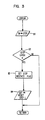
microcomputer 30 in Fig. 1 during fault mode operation. - Fig. 3 shows the step check subroutine used in the fault mode routine of Fig. 2.
- Referring now to the preferred embodiment of the invention in Fig. 1, a portion of the electronics to implement the invention are located on the diskette drive and the remaining portion is located on the adapter circuit card. The interface between the diskette drive and adapter circuit card is represented by the
dashed line 10. There are ten signal lines acrossinterface 10. All of the signal lines are shown, although only three of the lines, step, motor on, and read-data/fault-data, are used by the invention. - The interface between the using system and the adapter electronics card is represented by
dashed lines 12. The signal lines shown acrossinterface 12 are those signal lines necessary to understand the invention; other lines across the interface are not shown. -
Data bus 14 carries data to and fromdata register 16, status information fromstatus register 18, command information tocommand register 20 and recording head indexing information to step register/counter 21.Address bus 22 controls which of theregisters control lines 23A and 23B, respectively, from the using system control the reading and writing of information into or out of the registers. - The interrupt system signal over
line 24 is an interrupt flag to the using system. It indicates either that an operation has been completed by the adapter or the diskette drive or that there is a fault in the drive. -
Data register 16 in the adapter electronics is a buffer register for read data from the drive or for write data to the drive. Only the read data connection to the diskette drive is shown as that is the only portion relevant to the present invention. The read data signal from the drive is serial in form and is converted to an 8 bit word by serial toparallel converter 26. The clock signal used by theconverter 26 to do the conversion is the read clock signal derived from the recorded data signal by a phase lock loop (not shown) in the diskette drive. -
Status register 18 contains eight status bits of which only status bits 1, 2, and 7 (SB1, SB2, and SB7) are of interest to the invention. SB1 is a flag back to the using system that the present device is the diskette drive that has generated the interrupt. SB2 is a flag back to the using system that the interrupt was caused by a fault detected in the diskette drive. SB7 is the fault or error data and is passed back to the using system bit by bit as will be explained hereinafter. -
Command register 20 buffers commands from the using system anddecoder 28 decodes the commands for use by the adapter and the diskette drive. Commands relevant to the present invention are seek, device reset and reset interrupt. - The seek command is decoded by
decoder 28 to indicate the direction the recording head is to be moved and also to enable thestep clock 29 that generates the actual step pulses passed to the drive. The logic to generate the direction signal passed from the adapter to the drive is not shown as it is not relevant to the invention. The step pulses fromclock 29 are also used within the adapter to decrement the step count loaded into the step register/counter 21 by the using system. - The seek command is also decoded in
decoder 28 to generate a motor on (MTR ON) signal. The MTR ON signal is used to turn the spindle motor (disk motor) on and off. To prevent the recording head from scratching the recording disk, the MTR ON signal always goes active with the seek signal. Accordingly, the recording disk will always be moving when the recording head is moved across the disk. - The device reset and reset interrupt commands decoded by
decoder 28 are used by the adapter. Device reset is a more general reset command and would be used to reset all logic in the device to which it was sent. In the present invention, it is used to reset the interrupt signal and to reset the device from the fault mode. The reset interrupt is a limited reset signal and is only used to reset the interrupt system signal. - The step register/
counter 21 buffers the step count sent from the using system to the drive for the purpose of indexing the recording head. For each indexing operation, the using system sends a count to register/counter 21 equal to the number of steps the recording head is to be moved. After this count is read intoregister 21, the using system sends the seek command to commandregister 20 to start the indexing operation. - As described above, the seek command when decoded, causes
step clock 29 to emit the step pulses passed across the interface to the drive. Each step pulse also decrements the step count in register/counter 21. When the step count inregister 21 reaches zero, the register emits the seek complete signal that inhibitsstep clock 29 and sets the interruptsystem latch 58. The interrupt system signal coming up signals the using system that the adapter has finished the seek operation. - Referring now to the diskette drive in Fig. 1, an 8048
microcomputer 30 is used to control the drive. The step commands from the adapter are buffered throughlatch 32 before they are applied to thecomputer 30. When the computer has processed the step command from thelatch 32, it generates a signal online 34 to reset thestep latch 32. - The motor on (MTR ON) signal from the adapter is passed through a
buffer amplifier 36 tomicrocomputer 30.Computer 30 utilizes the motor on signal being active or present to activate thespindle motor drive 38. - Read Data (RD Data) is gated out of the diskette drive from a read/write channel (not shown) by the ready signal generated by
computer 30. The ready signal being present enables ANDgate 40 to pass the read data through OR 42 to the adapter. - In the event that a diagnostic routine performed by
computer 30 in the drive detects a fault or in the event a fault arises during operation,computer 30 drops the ready signal. ANDgate 40 is then inhibited and read data is not passed to the adapter. - When
computer 30 detects a fault and drops the ready signal to block read data, it also gates out a fault signal from the computer. This fault signal being present is the signal used by the adapter to detect the beginning of fault mode operation. - Referring to the adapter in Fig. 1, the detection of fault mode is accomplished by the
pulse width detector 46.Pulse width detector 46 receives a clock signal, used by the adapter and the diskette drive, having a frequency of 667 KHz. A clock signal of this frequency has a period equal to 1500 nanoseconds. Normal pulse width for read data varies between 300 and 900 nanoseconds, whereas the duration of the initial fault signal at one signal level is greater than 1500 nanoseconds. Therefore, when the fault signal is received via OR 42 in the diskette drive, thepulse width detector 46 will detect the fault condition because the signal's duration is greater than 1500 nanoseconds. - When the
pulse width detector 46 detects the fault signal, it generates an output signal that sets thefault mode latch 48. The fault mode latch output is used to gate fault or error data to status register 18, to generate the interrupt system signal atlatch 58 and to inhibit ANDgate 62 to prevent the motor on signal from being sent to the diskette drive. - The fault mode signal enables AND
gate 50 and after being inverted byinverter 52, inhibits ANDgate 54. ANDgate 54 normally passes the read data to the serial-to-parallel converter 26. ANDgate 50 passes fault data to status bit 7 of thestatus register 18. Thus, in fault mode, ANDgate 50 is active; otherwise ANDgate 54 is enabled. - The fault mode signal also is applied to status bit 2 (SB2) in the status register. This is a flag to the using system that the interrupt is due to a fault in the diskette drive. Fault mode also is passed by OR 56 to set the interrupt
latch 58. The interrupt latch is the source of the interrupt system signal online 24 passed back to the using system. - Finally, the fault mode signal via
inverter 60 inhibits ANDgate 62 from passing the motor on signal fromdecoder 28 to the diskette drive.Microcomputer 30 in the diskette drive interprets the absence of the motor on signal in combination with the presence of a step signal as a signal from the using system to gate out the first fault or error data bit fromregister 44 in the computer. Accordingly, in fault mode, the step signals received from the adapter by the diskette drive are used to shift out the successive bits making up the fault data stored atregister 44 incomputer 30. - Referring now to Fig. 2, the functions performed by the 8048
microcomputer 30 in Fig. 1 during fault mode operation are shown in the program flowchart. When the diskette drive has failed or diagnostic routines used by the computer have detected a fault in the diskette drive, the fault routine is entered. - At
functional block 70 in the fault routine, -computer 30 disables the external and timer/ counter interrupts that normally trigger the action and response cycles ofmicrocomputer 30. After the interrupts have been disabled,microcomputer 30 proceeds viafunctional block 72 to prepare the drive for the fault mode. - During
function 72, the computer generates signals on its output ports that disable the step motor drive 33 (Fig. 1) and the spindle motor drive 38 (Fig. 1). Also, duringblock 72 operation, the fault mode routine outputs the fault signal to OR 42 (Fig. 1) as previously described. Finally, function 72 in the routine resets the step latch 32 (Fig. 1). The result of the output functions performed bymicrocomputer 30 and represented byblock 72 is to set up the diskette drive for fault mode operation and to signal fault mode to the adapter by means of the fault signal. -
Microcomputer 30 then calls the step check (STPCHK) routine which is shown in detail in Fig. 3. The step check routine atinput function 90 checks an input port for the step signal fromstep latch 32. If the step signal is not present, the step check routine returns control to the routine that called it. If the step signal is present then program flow proceeds throughdecision block 92 to function 93 that sets a step received (STEP RECVD) flag.Next computer 30 atoutput function 94 emits the signal to resetstep latch 32. Afterfunction 94 program flow returns to the routine that called step check. - From the
step check routine 74, the fault mode routine goes todecision block 76 where it checks to see whether a step was received as flagged by thestep check routine 74. If it was not, then the program loops back to thestep check routine 74. If the step signal was received, the program branches to inputfunction 77. -
Function 77 looks at the MTR ON input port for the motor on signal.Decision 78 controls the program flow direction depending upon whether the motor on signal is active. If a motor on signal has been received, the fault mode has not been set in the adapter and the program loops back to thestep check routine 74 to look for the next step signal. If the motor on signal is not present, which is the normal sequence for fault mode, then the program branches tooutput function 80. - In
output function 80,microcomputer 30 shifts the first fault bit out of the computer to OR 42 and on to the adapter. As described earlier, this fault bit is passed by AND 50 in the adapter to status bit 7 ofstatus register 18. From thestatus register 18, the fault bit goes to the using system. The using system, when it detects the fault bit, generates another step command. - After the fault routine outputs the fault bit, the routine proceeds to call step check as represented by a
function 82. Step check again checks the appropriate input port for the step signal, sets the step received flag and resets the step latch if the step signal is received. Fromstep check 82, the fault mode routine proceeds todecision 84 where it checks for the step received flag. If a step was not received, program flow branches back to thestep check routine 82. If it was received, program flow proceeds to inputfunction 85 wheremicrocomputer 30 checks for the motor on signal. If motor on was not received,computer 30 knows that the step represents a command to shift another fault bit out of the computer sodecision 86 directs the program flow back tooutput function 80. Atfunction 80, the next fault bit is shifted fromcomputer 30 to OR 42 for passage to the adapter. - During
decision function 86, if themicrocomputer 30 detects a motor on signal present, the fault mode routine is exited to a normal power on reset (POR) supervisory program inmicroprocessor 30. The reception of a motor on signal at this point in the routine would indicate that the fault mode operation has finished and thefault mode latch 48 in Fig. 1 has been reset by a device reset command from the using system. - While the software routines used to control the
microcomputer 30 during operation of the invention have been described relative to the flowcharts in Figs. 2 and 3, the implementation in Assembler language for theINTEL 8048 microcomputer follow immediately hereafter. The first - line of code for portions of the program listing corresponding to the functional blocks in Figs. 2 and 3 have been identified with the same reference numerals used in Figs. 2 and 3.
-

- When the diskette drive is operating normally and read data is being passed back to the using system,
microcomputer 30 generates the ready signal that enables ANDgate 40. The read data then passes through ANDgate 40 and OR 42 in the diskette drive and through ANDgate 54 to the serial-to-parallel converter 26 in the adapter. - When
converter 26 has an 8 bit data word ready forregister 16, it passes it to the register. At the same time the DMA (Direct Memory Access)logic 27 in the adapter sends a request signal across the interface to the DMA controller in the using system. When the DMA controller can steal a cycle from the processor in the using system, it reads the eight bit word in data register 16 into the using system. Then the DMA controller sends an acknowledge signal back to theDMA logic 27 so that the logic will enableconverter 26 to load the next data word intoregister 16. Fault mode operation begins when themicrocomputer 30 in the diskette drive detects a failure in the functioning of the drive or the diagnostic routine performed at power on reset indicates a fault. If there is a failure in the drive, the diagnostic routines will automatically be initiated. - As a result of the diagnostic routines, an eight bit fault or error data word will be stored in
register 44 inmicrocomputer 30. The microcomputer shuts off its external and timer/counter interrupts and then outputs signals used to enter the fault mode. These output signals stop the stepper motor drive, stop spindle motor drive, inhibit the ready signal to ANDgate 40, reset thestep latch 32 and output the fault signal to OR 42. - At the adapter when the first fault signal is received, its duration is sufficient to trigger an output from the
pulse width detector 46.Pulse width detector 46 then sets latch 48 to indicate the fault mode operation to the adapter. - In fault mode operation at the adapter, AND
gate 50 is enabled and passes the first fault signal to status bit 7 of the status register. The fault mode signal fromlatch 48 also-sets the interrupt system latch 58-via-OR 56. The interrupt system signal is stored as status bit 1 (SB1) instatus register 18. " - In addition to setting interrupt
system latch 58, the fault mode signal also sets status bit SB2 in the status register and inhibits ANDgate 62 viainverter 60 from passing motor on signals tomicrocomputer 30 in the diskette drive. SB2 in the status register is an indication back to the using system that the interrupt is caused by a fault at the diskette drive. - When the using system receives the interrupt system signal over
line 24, it will scan the status registers in its peripheral devices looking for the device that generated the interrupt. As a result of addressingstatus register 18, the using system detects that SB1 is set, indicating the interrupt came from this peripheral device, and that SB2 is set indicating that a fault has occurred in the . diskette drive. - Knowing that the diskette drive and adapter are in the fault mode, the using system loads a reset interrupt command into
command register 20. The reset interrupt command resets latch 58 and the interrupt system signal drops. Then the using system loads a step count of one into step register/counter 21 and loads a seek command intocommand register 20. -
Decode 28 decodes the seek command an enables thestep clock 29. The clock pulse out ofstep clock 29 is the step signal that setslatch 32 in the diskette drive. In addition, this pulse counts down the step register/counter 21. Since the loaded count in register/counter 21 is one, register 21 is counted down to zero, andstep clock 29 is inhibited. - Zero count in
register 21 as previously described is the seek complete signal. The seek complete signal in addition to inhibitingstep clock 29, also setslatch 58 through OR 56. Accordingly, in interrupt system signal goes back to the using system overline 24 telling the system that the adapter has completed the seek or stepping operation. - In the diskette drive,
microcomputer 30 is now receiving a step signal fromstep latch 32 without the presence of a motor on signal (ANDgate 62 is inhibited). This combination of conditions indicates the adapter is in the fault mode. - Since the microcomputer is in the fault mode routine operation, the detection of the step signal and the not-active MTR ON signal causes the computer to output the first fault bit to OR 42. From OR 42, the fault bit passes through AND
gate 50 enabled by thefault mode latch 48 to status bit 7 (SB7) of thestatus register 18. - The using system having been interrupted by the interrupt system signal on
line 24 will generate a reset interrupt command to resetlatch 58. Then the using system addressesstatus register 18 and reads the contents of the register. In this case it is reading the register to pick out the fault bit at status bit 7. When the fault bit has been read from status bit 7 position, the using system loads a step count of one into register/counter 21 and loads a seek command intocommand register 20. The adapter and diskette drive are now prepared to read out the next fault bit from themicrocomputer 30. This cyclic process of reading one fault bit out, per step signal, from the microcomputer through the adapter to the using system continues until all eight fault bits have been read to the using system. - After the using system has read the entire fault data word, it sends a device reset command to the
command register 20.Decoder 28 decodes the device reset command and resets the interruptsystem latch 58 and thefault mode latch 48. - With the fault mode reset in the adapter, the using system next loads a step count of one into register/
counter 21 and loads a seek command intocommand register 20.Decode 28 generates the motor on signal and the seek signal from the seek command. Sincefault mode latch 48 has been reset, ANDgate 62 is enabled and allows the motor on signal to pass tomicrocomputer 30. The seek signal enablesstep clock 29, and the step clock passes the step signal to steplatch 32 in the diskette drive. - The fault mode routine (Fig. 2) detects that a step signal has been received and that MTR ON is active. Therefore, the routine exits to a Power On Reset routine (POR). The diskette drive and adapter are now back in normal data mode operation, and the fault data has been transferred from the diskette drive to the using system.
Claims (16)
Applications Claiming Priority (2)
| Application Number | Priority Date | Filing Date | Title |
|---|---|---|---|
| US06/439,956 US4521884A (en) | 1982-11-08 | 1982-11-08 | Method and apparatus for error data feedback in a diskette drive |
| US439956 | 1982-11-08 |
Publications (3)
| Publication Number | Publication Date |
|---|---|
| EP0108225A2 EP0108225A2 (en) | 1984-05-16 |
| EP0108225A3 EP0108225A3 (en) | 1985-01-16 |
| EP0108225B1 true EP0108225B1 (en) | 1987-03-11 |
Family
ID=23746813
Family Applications (1)
| Application Number | Title | Priority Date | Filing Date |
|---|---|---|---|
| EP83109322A Expired EP0108225B1 (en) | 1982-11-08 | 1983-09-20 | Apparatus and method for transferring fault data from a recording device to a data processor |
Country Status (4)
| Country | Link |
|---|---|
| US (1) | US4521884A (en) |
| EP (1) | EP0108225B1 (en) |
| JP (1) | JPS5987658A (en) |
| DE (1) | DE3370212D1 (en) |
Families Citing this family (3)
| Publication number | Priority date | Publication date | Assignee | Title |
|---|---|---|---|---|
| GB8518859D0 (en) * | 1985-07-25 | 1985-08-29 | Int Computers Ltd | Digital integrated circuits |
| JPH0439707A (en) * | 1990-06-06 | 1992-02-10 | Mitsubishi Electric Corp | Emergency stop device for numerical controller |
| US9830287B2 (en) * | 2015-02-24 | 2017-11-28 | Red Hat Israel, Ltd. | Determination of a device function asserting a detected spurious interrupt |
Family Cites Families (7)
| Publication number | Priority date | Publication date | Assignee | Title |
|---|---|---|---|---|
| US3704363A (en) * | 1971-06-09 | 1972-11-28 | Ibm | Statistical and environmental data logging system for data processing storage subsystem |
| US4101969A (en) * | 1977-06-06 | 1978-07-18 | Digital Equipment Corporation | Secondary storage facility with means for monitoring sector pulses |
| US4322813A (en) * | 1977-12-19 | 1982-03-30 | International Business Machines Corporation | Data log retrieval system |
| JPS6053339B2 (en) * | 1980-10-09 | 1985-11-25 | 日本電気株式会社 | Logical unit error recovery method |
| US4410942A (en) * | 1981-03-06 | 1983-10-18 | International Business Machines Corporation | Synchronizing buffered peripheral subsystems to host operations |
| US4435762A (en) * | 1981-03-06 | 1984-03-06 | International Business Machines Corporation | Buffered peripheral subsystems |
| JPS5823313A (en) * | 1981-07-31 | 1983-02-12 | Fujitsu Ltd | Information readout method in magnetic tape device |
-
1982
- 1982-11-08 US US06/439,956 patent/US4521884A/en not_active Expired - Fee Related
-
1983
- 1983-09-20 EP EP83109322A patent/EP0108225B1/en not_active Expired
- 1983-09-20 DE DE8383109322T patent/DE3370212D1/en not_active Expired
- 1983-10-11 JP JP58188586A patent/JPS5987658A/en active Granted
Also Published As
| Publication number | Publication date |
|---|---|
| EP0108225A3 (en) | 1985-01-16 |
| US4521884A (en) | 1985-06-04 |
| JPS5987658A (en) | 1984-05-21 |
| DE3370212D1 (en) | 1987-04-16 |
| JPS6343831B2 (en) | 1988-09-01 |
| EP0108225A2 (en) | 1984-05-16 |
Similar Documents
| Publication | Publication Date | Title |
|---|---|---|
| US3984814A (en) | Retry method and apparatus for use in a magnetic recording and reproducing system | |
| US4047157A (en) | Secondary storage facility for data processing | |
| CA1121068A (en) | Microcontroller for disk files | |
| US3999163A (en) | Secondary storage facility for data processing systems | |
| EP0468454B1 (en) | Interrupt controller | |
| US3688274A (en) | Command retry control by peripheral devices | |
| US3564502A (en) | Channel position signaling method and means | |
| US4253147A (en) | Memory unit with pipelined cycle of operations | |
| EP0059842A2 (en) | Data processing system with a plurality of peripheral devices | |
| US4500965A (en) | Capstanless magnetic tape drive with electronic equivalent to length of tape | |
| US4943907A (en) | Speed controller for recording and playback apparatus | |
| US3824563A (en) | Data storage track padding apparatus | |
| EP0108225B1 (en) | Apparatus and method for transferring fault data from a recording device to a data processor | |
| US3490013A (en) | Apparatus for detecting and eliminating noise records during a data transfer operation | |
| US3771125A (en) | Error correcting system of a magnetic tape unit | |
| US5459870A (en) | Interface circuit for controlling data transfers | |
| US4103327A (en) | Interrupt control circuit | |
| CA1124883A (en) | Microcontroller for disk files | |
| JPH07281836A (en) | Data transfer method | |
| JPH0423342B2 (en) | ||
| KR920001956B1 (en) | Floppy disk controller | |
| CA1124886A (en) | Microcontroller for disk files | |
| WO1989000313A1 (en) | Fast-tag transfer improvement | |
| JP2000187621A (en) | Scsi controller | |
| JPH03192425A (en) | Disk driving device |
Legal Events
| Date | Code | Title | Description |
|---|---|---|---|
| PUAI | Public reference made under article 153(3) epc to a published international application that has entered the european phase |
Free format text: ORIGINAL CODE: 0009012 |
|
| AK | Designated contracting states |
Designated state(s): DE FR GB IT |
|
| PUAL | Search report despatched |
Free format text: ORIGINAL CODE: 0009013 |
|
| 17P | Request for examination filed |
Effective date: 19840921 |
|
| AK | Designated contracting states |
Designated state(s): DE FR GB IT |
|
| GRAA | (expected) grant |
Free format text: ORIGINAL CODE: 0009210 |
|
| STAA | Information on the status of an ep patent application or granted ep patent |
Free format text: STATUS: THE PATENT HAS BEEN GRANTED |
|
| AK | Designated contracting states |
Kind code of ref document: B1 Designated state(s): DE FR GB IT |
|
| REF | Corresponds to: |
Ref document number: 3370212 Country of ref document: DE Date of ref document: 19870416 |
|
| ET | Fr: translation filed | ||
| ITF | It: translation for a ep patent filed |
Owner name: IBM - DR. ARRABITO MICHELANGELO |
|
| PLBE | No opposition filed within time limit |
Free format text: ORIGINAL CODE: 0009261 |
|
| 26N | No opposition filed | ||
| PGFP | Annual fee paid to national office [announced via postgrant information from national office to epo] |
Ref country code: GB Payment date: 19910823 Year of fee payment: 9 |
|
| PGFP | Annual fee paid to national office [announced via postgrant information from national office to epo] |
Ref country code: FR Payment date: 19910903 Year of fee payment: 9 |
|
| PGFP | Annual fee paid to national office [announced via postgrant information from national office to epo] |
Ref country code: DE Payment date: 19910926 Year of fee payment: 9 |
|
| ITTA | It: last paid annual fee | ||
| PG25 | Lapsed in a contracting state [announced via postgrant information from national office to epo] |
Ref country code: GB Effective date: 19920920 |
|
| GBPC | Gb: european patent ceased through non-payment of renewal fee |
Effective date: 19920920 |
|
| PG25 | Lapsed in a contracting state [announced via postgrant information from national office to epo] |
Ref country code: FR Effective date: 19930528 |
|
| PG25 | Lapsed in a contracting state [announced via postgrant information from national office to epo] |
Ref country code: DE Effective date: 19930602 |
|
| REG | Reference to a national code |
Ref country code: FR Ref legal event code: ST |