EP0104917B1 - Deflection system in an electron beam exposure device - Google Patents
Deflection system in an electron beam exposure device Download PDFInfo
- Publication number
- EP0104917B1 EP0104917B1 EP83305708A EP83305708A EP0104917B1 EP 0104917 B1 EP0104917 B1 EP 0104917B1 EP 83305708 A EP83305708 A EP 83305708A EP 83305708 A EP83305708 A EP 83305708A EP 0104917 B1 EP0104917 B1 EP 0104917B1
- Authority
- EP
- European Patent Office
- Prior art keywords
- bits
- converters
- circuit
- data
- electron beam
- Prior art date
- Legal status (The legal status is an assumption and is not a legal conclusion. Google has not performed a legal analysis and makes no representation as to the accuracy of the status listed.)
- Expired
Links
Images


Classifications
-
- H—ELECTRICITY
- H10—SEMICONDUCTOR DEVICES; ELECTRIC SOLID-STATE DEVICES NOT OTHERWISE PROVIDED FOR
- H10P—GENERIC PROCESSES OR APPARATUS FOR THE MANUFACTURE OR TREATMENT OF DEVICES COVERED BY CLASS H10
- H10P95/00—Generic processes or apparatus for manufacture or treatments not covered by the other groups of this subclass
-
- H—ELECTRICITY
- H03—ELECTRONIC CIRCUITRY
- H03M—CODING; DECODING; CODE CONVERSION IN GENERAL
- H03M1/00—Analogue/digital conversion; Digital/analogue conversion
- H03M1/66—Digital/analogue converters
- H03M1/74—Simultaneous conversion
Definitions
- the present invention relates to a deflection system and more particularly to digital-to-analog (D/A) converters in the deflection system of an electron beam exposure device.
- D/A digital-to-analog
- Digital-to-analog converters used in the deflection system of an electron beam exposure device must be capable of converting data consisting of 18 to 20 bits.
- conventional D/A converters are simply contructed only to a degree which renders them capable of converting data consisting of 12 to 14 bits.
- data consisting of the most significant bits, i.e., m bits is decoded so as to turn on S constant-current (voltage) sources among 2m constant-current (voltage) sources, and data consisting of the least significant bits, i.e., n-m bits, is input into the D/A converters so as to add the outputs in an analog manner.
- the mismatching of the weighting of bits occurs when the data changes, for example, from 01111 to 10000, and deflection of the electron beam must be interrupted when the mismatching phenomenon occurs.
- the mismatching of bits occurs due to the mismatching of the weighting of the resistances of switching transistors which work to convert binary signals into analog signal, and the pattern which is described becomes locally narrowed or widened.
- a Gritch phenomenon occurs due to the simultaneous switching of data having different weighting values.
- D/A converter which is capable of maintaining monotone increase through simple adjustment. It is also desirable to provide a D/A converter which can prevent the mismatching of the weighting of bits.
- GB-A-2 069 265 discloses an R-2R type D/ A converter having a resistor network which generates a number of equally weighted currents selectively switched to an output bus to provide the analogue output.
- the binary digital input is decoded into a special code such that an incremental increase in the input causes an additional one of the equally weighted currents to be coupled to the output bus.
- a deflection system in an electron beam exposure device including digital-to-analogue (D/A) conversion circuitry, comprising decoding circuitry and a plurality of D/A converters and arranged for converting n-bit input digital data to an analogue output signal for supply to a deflection means wherein the m most significant bits of the input digital data are supplied to the decoding circuitry and the (n-m) least significant bits are supplied to the D/A converters; characterised in that:
- Figure 1 is a schematic view of an example of a conventional electron beam exposure device.
- reference numerals 1, 2, and 3 designate a cathode, a grid, and an anode, respectively, constituting an electron gun.
- Reference numeral 4 designates a deflection unit for blanking an electron beam, 5 a first diaphragm having a first aperture of a polygon, 6 an electron lens, 7 a deflection unit for controlling the position of the images formed by the electron lens 6 on a second diaphragm 8 having a second aperture of a polygon for deflecting the beam passed through the first diaphragm 5, 9 a de-magnifying lens, 10 a focusing lens, and 11 a deflection unit for positioning a shaped beam formed on a sample of, for example, a semiconductor wafer on which a resist is coated.
- the D/A converters used in the deflection systems 7 and 11 of the electron beam exposure device shown in Fig. 1 must be capable of converting data consisting of 18 to 20 bits.
- the D/A converters are simply constructed to a degree capable of converting data consisting of 12 to 14 bits.
- data consisting of m bits is decoded to turn on S constant current (voltage) sources among 2 m constant-current (voltage) sources, and data consisting of n-m bits is input into the D/A converter to add the outputs in an analog manner.
- the mismatching of the weighting of bits occurs when the data changes, for example, from 01111 to 10000, as is shown in Fig. 2, and deflection of the electron beam must be interrupted when the mismatching phenomenon occurs.
- the mismatching of bits occurs due to the mismatching of the weighting resistances of the switching transistors which work to convert binary signals into analog signals, and the pattern which is described becomes locally narrowed or widened.
- a D/ A converter for deflection of an electron beam comprises a plurality of small converters, and the input/output data is all successively rendered to be "1", beginning with the first D/A converter, so as to prevent the Gritch phenomenon.
- This circuit connection is illustrated in Fig. 3.
- the input data 21 is divided into m bits and n-m bits.
- the m bits are applied to a decoder circuit 22 which sends an output to a gate circuit 1 (23A), a gate circuit 2 (23B), - - -, and a gate circuit 2 m (23N).
- the n-m bits are applied to a D/A converter 1 (24A), a D/A conveter 2 (24B), - - -, a D/ A converter 2m (24N) via the gate circuit 1 (23A), the gate circuit 2 (23B), - - -, and the gate circuit 2 m (23N), respectively.
- the number 2m of D/A converters corresponds to the number of m bits. Furthermore, the m bits are applied to a D/A converter 25, outputs of the D/A converters 24A, 24B, ---, 24N, and 25 are added by an amplifier 26, and the sum is applied to a deflection coil 27.
- the decoder circuit consists of a binary-hexadecimal converter which converts a binary code consisting of 4 bits into a hexadecimal number.
- the thus-converted output is applied to the gate circuits 23A, 23B, - - -, and 23N.
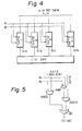
- Figure 4 illustrates the gate circuits 23A, 23B, ---, and 23N in detail, in which the gates 31A, 31B, - - -, and 31 N receive outputs Ai and Bi from the decoder circuit 22 and data consisting of n-m bits.
- each of the gates 31A, 31B, ---, and 31 N consists of AND circuits AND 1, AND 2, and AND 3 and an OR circuit OR.
- the symbols A o , B 0 , A 1 , --- at the top of the figure represent outputs of the decoder circuit 22
- the numerals 0: 0000, 1: 0001, - - - at the left of the figure represent inputs of the decoder circuit 22
- the numerals at the right of the figure represent outputs of the D/A converters 24A, 24B, - - -, 24N that correspond to the inputs 0: 0000, 1: 0001, - - - of the decoder circuit 22.
- the D/A converter 25 has the following function. Namely, in the D/A converter 2 m , a step 00001111 usually has the same level as a step 00010000, and, hence, one step is lost.
- the D/A converter 25 functions as an adjusting circuit which provides a difference of one step between the level 00001111 and the level 00010000.
- an electron beam exposure device which requires only simple adjustment and which assures a monotone increase.
Landscapes
- Electron Beam Exposure (AREA)
- Exposure And Positioning Against Photoresist Photosensitive Materials (AREA)
- Analogue/Digital Conversion (AREA)
Applications Claiming Priority (2)
| Application Number | Priority Date | Filing Date | Title |
|---|---|---|---|
| JP166708/82 | 1982-09-27 | ||
| JP57166708A JPS5956727A (ja) | 1982-09-27 | 1982-09-27 | 電子ビ−ム露光装置 |
Publications (3)
| Publication Number | Publication Date |
|---|---|
| EP0104917A2 EP0104917A2 (en) | 1984-04-04 |
| EP0104917A3 EP0104917A3 (en) | 1987-01-14 |
| EP0104917B1 true EP0104917B1 (en) | 1989-11-23 |
Family
ID=15836282
Family Applications (1)
| Application Number | Title | Priority Date | Filing Date |
|---|---|---|---|
| EP83305708A Expired EP0104917B1 (en) | 1982-09-27 | 1983-09-26 | Deflection system in an electron beam exposure device |
Country Status (4)
| Country | Link |
|---|---|
| US (1) | US4583077A (pl) |
| EP (1) | EP0104917B1 (pl) |
| JP (1) | JPS5956727A (pl) |
| DE (1) | DE3380892D1 (pl) |
Families Citing this family (5)
| Publication number | Priority date | Publication date | Assignee | Title |
|---|---|---|---|---|
| US4998108A (en) * | 1990-07-30 | 1991-03-05 | International Business Machines Corporation | Large range, high speed, high accuracy digital-to-analog converter |
| US5784019A (en) * | 1997-01-30 | 1998-07-21 | National Semiconductor Corporation | Digital to analog converter for generating distributive analog control signals utilizing digital signal generator and control signal generator |
| US6133987A (en) * | 1998-10-22 | 2000-10-17 | Nikon Corporation | Technique for reducing pattern placement error in projection electron-beam lithography |
| DE202011108664U1 (de) | 2011-12-06 | 2013-03-07 | Ziegelmundstückbau Braun GmbH | Mundstück |
| JP2016096204A (ja) * | 2014-11-13 | 2016-05-26 | 株式会社ニューフレアテクノロジー | 出力調整方法及び電子線描画装置 |
Family Cites Families (4)
| Publication number | Priority date | Publication date | Assignee | Title |
|---|---|---|---|---|
| US4338592A (en) * | 1980-02-11 | 1982-07-06 | Hybrid Systems Corporation | High accuracy digital-to-analog converter and transient elimination system thereof |
| US4412208A (en) * | 1980-09-16 | 1983-10-25 | Nippon Telegraph & Telephone Public Corporation | Digital to analog converter |
| JPS57194625A (en) * | 1981-05-27 | 1982-11-30 | Nec Corp | Digital to analog converter |
| US4430642A (en) * | 1981-10-02 | 1984-02-07 | Westinghouse Electric Corp. | Digital-to-analog converter |
-
1982
- 1982-09-27 JP JP57166708A patent/JPS5956727A/ja active Granted
-
1983
- 1983-09-26 DE DE8383305708T patent/DE3380892D1/de not_active Expired
- 1983-09-26 EP EP83305708A patent/EP0104917B1/en not_active Expired
- 1983-09-27 US US06/536,467 patent/US4583077A/en not_active Expired - Fee Related
Also Published As
| Publication number | Publication date |
|---|---|
| JPS6325497B2 (pl) | 1988-05-25 |
| EP0104917A3 (en) | 1987-01-14 |
| JPS5956727A (ja) | 1984-04-02 |
| DE3380892D1 (en) | 1989-12-28 |
| EP0104917A2 (en) | 1984-04-04 |
| US4583077A (en) | 1986-04-15 |
Similar Documents
| Publication | Publication Date | Title |
|---|---|---|
| US5243347A (en) | Monotonic current/resistor digital-to-analog converter and method of operation | |
| US4430642A (en) | Digital-to-analog converter | |
| US5283579A (en) | Digital to analog converter having high multiplying bandwidth | |
| CA1192311A (en) | High resolution digital-to-analog converter | |
| US8599057B2 (en) | Digital-to-analog converter | |
| EP0066251B1 (en) | Digital to analog converter | |
| US5801655A (en) | Multi-channel D/A converter utilizing a coarse D/A converter and a fine D/A converter | |
| US6741195B1 (en) | Low glitch current steering digital to analog converter and method | |
| US4338592A (en) | High accuracy digital-to-analog converter and transient elimination system thereof | |
| US5867116A (en) | Multi-stage interpolating analog-to-digital conversion | |
| KR100845746B1 (ko) | 면적을 최소화하는 디지털-아날로그 변환기 및 그것을포함하는 소스 드라이버 | |
| US4450433A (en) | D/A Converting circuit having two D/A converters for decoding and converting a digital signal into an analog signal | |
| US5231398A (en) | Method and apparatus for self-tracking multiple analog to digital conversion | |
| EP0708530A1 (en) | Current source driven DA converter and AD using the same | |
| US4712091A (en) | Digital/analog converter having a switchable reference current | |
| US4695826A (en) | High accuracy digital-to-analog converter having symmetrical current source switching | |
| EP0322965A1 (en) | Digital-to-analog converter | |
| EP0104917B1 (en) | Deflection system in an electron beam exposure device | |
| US3995266A (en) | Device for setting an electric command variable | |
| US6154160A (en) | Circuit arrangement including digital-to-analog current converters | |
| JPH1093436A (ja) | デジタル・アナログ変換回路 | |
| EP0252321A2 (en) | Digital-to-analog converter with gain compensation | |
| US4250492A (en) | Non-uniform weighting circuitry | |
| GB2029143A (en) | Digital to analogue converter | |
| US4410880A (en) | Digital-to-analog converter and analog-to-digital converter with controllable bi-polar and uni-polar capability |
Legal Events
| Date | Code | Title | Description |
|---|---|---|---|
| PUAI | Public reference made under article 153(3) epc to a published international application that has entered the european phase |
Free format text: ORIGINAL CODE: 0009012 |
|
| AK | Designated contracting states |
Designated state(s): DE FR GB |
|
| PUAL | Search report despatched |
Free format text: ORIGINAL CODE: 0009013 |
|
| AK | Designated contracting states |
Kind code of ref document: A3 Designated state(s): DE FR GB |
|
| 17P | Request for examination filed |
Effective date: 19870618 |
|
| 17Q | First examination report despatched |
Effective date: 19871229 |
|
| GRAA | (expected) grant |
Free format text: ORIGINAL CODE: 0009210 |
|
| AK | Designated contracting states |
Kind code of ref document: B1 Designated state(s): DE FR GB |
|
| ET | Fr: translation filed | ||
| REF | Corresponds to: |
Ref document number: 3380892 Country of ref document: DE Date of ref document: 19891228 |
|
| PLBE | No opposition filed within time limit |
Free format text: ORIGINAL CODE: 0009261 |
|
| STAA | Information on the status of an ep patent application or granted ep patent |
Free format text: STATUS: NO OPPOSITION FILED WITHIN TIME LIMIT |
|
| 26N | No opposition filed | ||
| PGFP | Annual fee paid to national office [announced via postgrant information from national office to epo] |
Ref country code: GB Payment date: 19920707 Year of fee payment: 10 |
|
| PGFP | Annual fee paid to national office [announced via postgrant information from national office to epo] |
Ref country code: FR Payment date: 19920929 Year of fee payment: 10 |
|
| PGFP | Annual fee paid to national office [announced via postgrant information from national office to epo] |
Ref country code: DE Payment date: 19921125 Year of fee payment: 10 |
|
| PG25 | Lapsed in a contracting state [announced via postgrant information from national office to epo] |
Ref country code: GB Effective date: 19930926 |
|
| GBPC | Gb: european patent ceased through non-payment of renewal fee |
Effective date: 19930926 |
|
| PG25 | Lapsed in a contracting state [announced via postgrant information from national office to epo] |
Ref country code: FR Free format text: LAPSE BECAUSE OF NON-PAYMENT OF DUE FEES Effective date: 19940531 |
|
| PG25 | Lapsed in a contracting state [announced via postgrant information from national office to epo] |
Ref country code: DE Effective date: 19940601 |
|
| REG | Reference to a national code |
Ref country code: FR Ref legal event code: ST |