EP0104865A2 - Codebestätigungskreis - Google Patents
Codebestätigungskreis Download PDFInfo
- Publication number
- EP0104865A2 EP0104865A2 EP83305506A EP83305506A EP0104865A2 EP 0104865 A2 EP0104865 A2 EP 0104865A2 EP 83305506 A EP83305506 A EP 83305506A EP 83305506 A EP83305506 A EP 83305506A EP 0104865 A2 EP0104865 A2 EP 0104865A2
- Authority
- EP
- European Patent Office
- Prior art keywords
- counter
- circuit
- switches
- output
- sequence
- Prior art date
- Legal status (The legal status is an assumption and is not a legal conclusion. Google has not performed a legal analysis and makes no representation as to the accuracy of the status listed.)
- Withdrawn
Links
- 238000012790 confirmation Methods 0.000 title claims abstract description 8
- 230000004048 modification Effects 0.000 description 3
- 238000012986 modification Methods 0.000 description 3
- 238000010586 diagram Methods 0.000 description 2
- 238000000034 method Methods 0.000 description 2
- 239000003990 capacitor Substances 0.000 description 1
- 230000000994 depressogenic effect Effects 0.000 description 1
Images
Classifications
-
- G—PHYSICS
- G07—CHECKING-DEVICES
- G07C—TIME OR ATTENDANCE REGISTERS; REGISTERING OR INDICATING THE WORKING OF MACHINES; GENERATING RANDOM NUMBERS; VOTING OR LOTTERY APPARATUS; ARRANGEMENTS, SYSTEMS OR APPARATUS FOR CHECKING NOT PROVIDED FOR ELSEWHERE
- G07C9/00—Individual registration on entry or exit
- G07C9/00174—Electronically operated locks; Circuits therefor; Nonmechanical keys therefor, e.g. passive or active electrical keys or other data carriers without mechanical keys
- G07C9/00658—Electronically operated locks; Circuits therefor; Nonmechanical keys therefor, e.g. passive or active electrical keys or other data carriers without mechanical keys operated by passive electrical keys
- G07C9/00674—Electronically operated locks; Circuits therefor; Nonmechanical keys therefor, e.g. passive or active electrical keys or other data carriers without mechanical keys operated by passive electrical keys with switch-buttons
- G07C9/0069—Electronically operated locks; Circuits therefor; Nonmechanical keys therefor, e.g. passive or active electrical keys or other data carriers without mechanical keys operated by passive electrical keys with switch-buttons actuated in a predetermined sequence
Definitions
- This invention relates to a code confirmation circuit, that is to a circuit arranged to confirm, or otherwise, that an input denoted by a sequence of switch operations agrees with a predetermined code sequence.
- a code confirmation circuit that is to a circuit arranged to confirm, or otherwise, that an input denoted by a sequence of switch operations agrees with a predetermined code sequence.
- Such a circuit may be used, for example, with a so-called "digital lock" in which the operation of a number of keys in the correct sequence is necessary for the release of the lock. The keys are frequently, though not necessarily, marked with digits, though other symbols are sometimes used,
- a code confirmation circuit which includes input means comprising a number of switches each representing a different code value, a counter having a number of outputs energisable in sequence from a datum state and each corresponding to a different code value, circuit means interconnecting the said switches and the said counter outputs such that the operation of a switch having the same code value as an energised counter output causes the counter to be clocked so as to energise the next counter output in the sequence, and resetting means responsive to the operation of a switch having a code value different from that of an energised counter output to prevent the clocking of the counter to the next output in sequence, the energisation of the last counter output in the sequence indicating the confirmation of the code identified by the sequence in which the switches were operated.
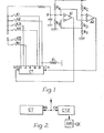
- FIG. 1 shows a simple circuit according to the invention.
- the switches are in the form of push-button keys of which only six are shown.
- a counter CT has each of its outputs connected directly through a separate and predetermined one of the keys Kl to Kn to a common point P.
- a capacitor is connected to point P to remove transients caused by key contact bounce.
- a first amplifier Al has its non-inverting input connected to point P and to a potential divider comprising resistors R A and R B , and has its non-inverting input connected to a reference voltage V Rl derived from a further potential divider comprising resistors R C , R D and R E .
- the output of amplifier Al is connected to the reset input RS of the counter CT.
- a second amplifier A2 has its inverting input connected to the common point P, and has its non-inverting input connected to a second reference voltage V R2 , also derived from the further potential divider, which is higher than V R1 .
- the output of amplifier A2 is connected to the clock,input CK of the counter CT.
- the last output of the counter CT is connected to some form of actuator, shown here as a relay RL, to operate whatever mechanism or circuit is controlled by the circuit.
- the counter In operation, the counter is normally reset to its '0' state, with the '0' output of the counter in the high state and awaiting operation of the keys. If the key connected to this output, shown in the drawing as key K8, is pressed, then the non-inverting input of amplifier Al also goes high. This causes no change in the amplfier output. Similarly, the inverting input of the amplifier A2 goes low on key closure. This change does affect the counter, but the subsequent change when the key K8 is released results in the output of amplifier A2 going high and causing the counter CT to clock so as to energise the '1' output of the counter. The above procedure is followed each time that a key is operated in the correct sequence, this sequence being determined purely by the interconnections between the keys and the counter outputs.
- Figure 2 shows a modification of the circuit of Figure 1 to include a second counter CT1 arranged to render the circuit inoperative, or give an alarm, after a predetermined number of errors.
- This second counter is clocked by the "reset" signals from amplifier Al of Figure 1, and an output from the counter CT2 after a predetermined number of input signals operates a lock-out or alarm circuit AM.
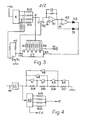
- Figure 3 shows a second embodiment which allows for a larger number of possible code combinations by allowing each key to be used as many times as required. Such an arrangement having ten keys will provide 10 10 possible combinations.
- each output except the '0' state output is connected to the common point P through a separate resistor Rl to R9 of predetermined value.
- Also connected to the common point P are four resistors R10 to R13 connected to a voltage source -V by way of a conventional binary-coded decimal keyboard K.
- the keyboard is arranged to connect one or more of the resistors R10 to R13 to the voltage source, depending on which key is operated.
- Each output from the keyboard K is also connected through resistors to a transistor inverter Q 1 connected to the clock input CK of the counter CT.
- the clock input CK is also connected to the control input of a switch Q 2 .
- the common point P is also connected by switch Q 2 to the inverting input of an amplifier Al having its non-inverting input connected to a reference voltage V R , preferably zero.
- the output of amplifier Al is connected to the inverting input of a second amplifier A2, again having its non-inverting input connected to the same reference voltage V R .
- the outputs of the two amplifiers Al and A2 are connected through diodes Dl and D2 to the reset input RS of the counter CT.
- the output of the last stage of the counter is connected to an actuator, such as a relay RL, or to another circuit or circuit element.
- each successive output of the counter CT from the datum or '0' state represents a different successive code value. If, for example, nine keys provide nine decimal digits, and the counter CT is a ten stage counter, then the code will have nine digits, each being represented by a different output from the counter. When the counter is in any particular state, then current from the counter output will flow through the energised one of the resistors Rl to R9, causing a voltage to exist at the common point P. Equally, when one of the keys of the keyboard is pressed, a particular voltage will be developed across the selected one or ones of the resistors R10 to R13 and applied to the common point P.
- the resistors Rl to R9 are thus chosen so that the voltage developed across the nth one is equal and opposite to the voltage developed at point P resulting from the operation of the key representing the nth digit in the code sequence.
- the counter is again clocked, to energise resistor R2. Again, if the voltage developed across them is arranged to be equal and opposite to that developed across resistor R10 then the counter CT will not be reset.
- the process may be repeated throughout the code sequence, until the output from the last stage of the counter shows that the required number of keys have been pressed in the correct sequence, and the actuator RL is energised.
- circuit described above gives the full range of 9 possible combinations. Simpler or shorter sequences may obviously be used by using codes having a shorter sequence of digits. Each digit may be used in the sequence as often as required, or not used at all.
- Figure 4 shows such an arrangement which may be connected into such a loop system.
- the main difference from the circuit of Figure 3 is the modified connection of the keyboard and the inclusion of an analog-to-digital converter AD, and a constant current generator CC.
- the switches may be in the form of push-button keys, of which only six are shown, labelled Kl to K6. These switches are connected across four resistors R14 to R17 connected in series with one another.
- the values of the resistors are such that any series connection of one or more of the resistors will give an unique total resistance value.
- the resistors may have resistance values related by a binary sequence, such as N, 2N, 4N and 8N. With the appropriate connection of the switches K, these resistors would give up to sixteen unique resistance values on the operation of a single one of the switches.
- the series-connected resistors are connected across the output of the constant current generator CC.
- the voltage generated across the series-connected resistors R14 to R17, or any of those resistors, is applied to the input of a four-bit analog-to-digital converter AD.
- the four outputs of the converter are each connected through separate resistors R10 to R13 to the common point P.
- the counter CT and amplifiers Al and A2 are connected as shown in Figure 3, and the circuit operates in a similar manner.
- a voltage developed across one or more of resistors R14 to R17 produce a particular combination of outputs from the converter AD, resulting in a voltage at point P unique to the code value of the depressed key. As before, for correct operation this voltage is offset by the voltage developed across the resistor connected to the energised counter output.
- lock-out or alarm circuit may be added to this embodiment.
Landscapes
- Physics & Mathematics (AREA)
- General Physics & Mathematics (AREA)
- Programmable Controllers (AREA)
- Input From Keyboards Or The Like (AREA)
- Lock And Its Accessories (AREA)
Applications Claiming Priority (2)
| Application Number | Priority Date | Filing Date | Title |
|---|---|---|---|
| GB08227635A GB2128003B (en) | 1982-09-28 | 1982-09-28 | Code confirmation circuit |
| GB8227635 | 1982-09-28 |
Publications (2)
| Publication Number | Publication Date |
|---|---|
| EP0104865A2 true EP0104865A2 (de) | 1984-04-04 |
| EP0104865A3 EP0104865A3 (de) | 1984-12-27 |
Family
ID=10533213
Family Applications (1)
| Application Number | Title | Priority Date | Filing Date |
|---|---|---|---|
| EP83305506A Withdrawn EP0104865A3 (de) | 1982-09-28 | 1983-09-20 | Codebestätigungskreis |
Country Status (4)
| Country | Link |
|---|---|
| EP (1) | EP0104865A3 (de) |
| JP (1) | JPS5980874A (de) |
| ES (1) | ES8405994A1 (de) |
| GB (1) | GB2128003B (de) |
Cited By (1)
| Publication number | Priority date | Publication date | Assignee | Title |
|---|---|---|---|---|
| EP0921452A1 (de) * | 1997-12-03 | 1999-06-09 | Ford Motor Company | Benutzerschnittstellenarchitektur zur Steuerung von elektronischen Fahrzeugsystemen |
Family Cites Families (3)
| Publication number | Priority date | Publication date | Assignee | Title |
|---|---|---|---|---|
| GB1323542A (en) * | 1971-01-13 | 1973-07-18 | Shorrock Dev | Electric combination lock |
| US3831065A (en) * | 1973-04-06 | 1974-08-20 | Integrated Conversion Tech | Electronic push button combination lock |
| US3846756A (en) * | 1973-06-25 | 1974-11-05 | Westinghouse Electric Corp | Programmable sequential logic circuit |
-
1982
- 1982-09-28 GB GB08227635A patent/GB2128003B/en not_active Expired
-
1983
- 1983-09-20 EP EP83305506A patent/EP0104865A3/de not_active Withdrawn
- 1983-09-27 ES ES525979A patent/ES8405994A1/es not_active Expired
- 1983-09-28 JP JP18174983A patent/JPS5980874A/ja active Pending
Cited By (2)
| Publication number | Priority date | Publication date | Assignee | Title |
|---|---|---|---|---|
| EP0921452A1 (de) * | 1997-12-03 | 1999-06-09 | Ford Motor Company | Benutzerschnittstellenarchitektur zur Steuerung von elektronischen Fahrzeugsystemen |
| US6005488A (en) * | 1997-12-03 | 1999-12-21 | Ford Motor Company | User control interface architecture for automotive electronic systems |
Also Published As
| Publication number | Publication date |
|---|---|
| GB2128003A (en) | 1984-04-18 |
| JPS5980874A (ja) | 1984-05-10 |
| GB2128003B (en) | 1986-06-18 |
| ES525979A0 (es) | 1984-06-16 |
| ES8405994A1 (es) | 1984-06-16 |
| EP0104865A3 (de) | 1984-12-27 |
Similar Documents
| Publication | Publication Date | Title |
|---|---|---|
| JPS60222949A (ja) | モジユ−ルの存在センサ | |
| GB1040614A (en) | Improvements in or relating to code translation systems | |
| EP0436555A4 (en) | Error limiting analog to digital converter | |
| US5179560A (en) | Apparatus for decoding bch code for correcting complex error | |
| GB1567023A (en) | Controlled electrical supply arrangements | |
| EP0104865A2 (de) | Codebestätigungskreis | |
| US3965469A (en) | Annunciator structure and method | |
| GB904225A (en) | Improvements in or relating to digital servo system | |
| US3348198A (en) | Code-checking comparator circuit | |
| US2994862A (en) | Digital to analog conversion | |
| EP0286796B1 (de) | Parallelvergleichstyp-AD-Wandler mit Fehlerunterdrückung | |
| US3059223A (en) | Analog-to-digital converter | |
| US3453615A (en) | Analog-to-digital converters | |
| GB941351A (en) | Improvements in or relating to circuit arrangements for the conversion of analogue values into binary numbers | |
| GB1599768A (en) | Design of fail safe electronic circuitry | |
| US3500321A (en) | Electronic digital comparator | |
| US3722107A (en) | Circuit arrangement for code checking and code transforming | |
| US3626407A (en) | Circuits for conversion between analog and digital representations of data | |
| US3064247A (en) | Electrical measuring apparatus | |
| EP0061616B1 (de) | Fehlerprüfung von sich gegenseitig ausschliessenden Steuersignalen | |
| JPH028760A (ja) | 半導体集積回路装置 | |
| US4199727A (en) | Malfunction detector | |
| JPH0227401A (ja) | オフセット制御回路 | |
| SU1441438A1 (ru) | Устройство дистанционного управлени | |
| SU1039029A1 (ru) | Декодирующа матрица |
Legal Events
| Date | Code | Title | Description |
|---|---|---|---|
| PUAI | Public reference made under article 153(3) epc to a published international application that has entered the european phase |
Free format text: ORIGINAL CODE: 0009012 |
|
| AK | Designated contracting states |
Designated state(s): CH DE FR IT LI SE |
|
| PUAL | Search report despatched |
Free format text: ORIGINAL CODE: 0009013 |
|
| AK | Designated contracting states |
Designated state(s): CH DE FR IT LI SE |
|
| 17P | Request for examination filed |
Effective date: 19850827 |
|
| STAA | Information on the status of an ep patent application or granted ep patent |
Free format text: STATUS: THE APPLICATION IS DEEMED TO BE WITHDRAWN |
|
| 18D | Application deemed to be withdrawn |
Effective date: 19860402 |