EP0104761B1 - Daten- und Taktrückgewinnungssystem für Datenübertragungssteuerungseinrichtung - Google Patents
Daten- und Taktrückgewinnungssystem für Datenübertragungssteuerungseinrichtung Download PDFInfo
- Publication number
- EP0104761B1 EP0104761B1 EP83304859A EP83304859A EP0104761B1 EP 0104761 B1 EP0104761 B1 EP 0104761B1 EP 83304859 A EP83304859 A EP 83304859A EP 83304859 A EP83304859 A EP 83304859A EP 0104761 B1 EP0104761 B1 EP 0104761B1
- Authority
- EP
- European Patent Office
- Prior art keywords
- data
- delay
- transitions
- data packet
- transition
- Prior art date
- Legal status (The legal status is an assumption and is not a legal conclusion. Google has not performed a legal analysis and makes no representation as to the accuracy of the status listed.)
- Expired
Links
- 238000011084 recovery Methods 0.000 title claims description 42
- 238000004891 communication Methods 0.000 title claims description 25
- 230000007704 transition Effects 0.000 claims description 70
- 238000000034 method Methods 0.000 claims description 6
- 230000005540 biological transmission Effects 0.000 description 14
- 239000000872 buffer Substances 0.000 description 7
- 238000010586 diagram Methods 0.000 description 7
- 230000003111 delayed effect Effects 0.000 description 6
- 230000001419 dependent effect Effects 0.000 description 6
- 238000005070 sampling Methods 0.000 description 6
- 230000000694 effects Effects 0.000 description 5
- 238000005516 engineering process Methods 0.000 description 5
- 230000000295 complement effect Effects 0.000 description 4
- 239000004065 semiconductor Substances 0.000 description 4
- 101100172132 Mus musculus Eif3a gene Proteins 0.000 description 3
- 239000003990 capacitor Substances 0.000 description 3
- 238000013016 damping Methods 0.000 description 3
- 238000001514 detection method Methods 0.000 description 3
- 230000000873 masking effect Effects 0.000 description 3
- 238000012545 processing Methods 0.000 description 3
- 230000008901 benefit Effects 0.000 description 2
- 230000008859 change Effects 0.000 description 2
- 125000004122 cyclic group Chemical group 0.000 description 2
- 238000004519 manufacturing process Methods 0.000 description 2
- 101100001669 Emericella variicolor andD gene Proteins 0.000 description 1
- 230000003139 buffering effect Effects 0.000 description 1
- 239000000969 carrier Substances 0.000 description 1
- 238000006243 chemical reaction Methods 0.000 description 1
- 238000010276 construction Methods 0.000 description 1
- 238000011161 development Methods 0.000 description 1
- 238000009792 diffusion process Methods 0.000 description 1
- 238000007667 floating Methods 0.000 description 1
- 230000005764 inhibitory process Effects 0.000 description 1
- 238000002955 isolation Methods 0.000 description 1
- 238000012423 maintenance Methods 0.000 description 1
- 230000007257 malfunction Effects 0.000 description 1
- 239000013307 optical fiber Substances 0.000 description 1
- 238000005457 optimization Methods 0.000 description 1
- 230000010363 phase shift Effects 0.000 description 1
- 230000000704 physical effect Effects 0.000 description 1
- 230000000135 prohibitive effect Effects 0.000 description 1
- 230000009467 reduction Effects 0.000 description 1
- 230000003362 replicative effect Effects 0.000 description 1
- 230000011664 signaling Effects 0.000 description 1
- 238000000638 solvent extraction Methods 0.000 description 1
- 230000001360 synchronised effect Effects 0.000 description 1
Images




Classifications
-
- H—ELECTRICITY
- H03—ELECTRONIC CIRCUITRY
- H03L—AUTOMATIC CONTROL, STARTING, SYNCHRONISATION OR STABILISATION OF GENERATORS OF ELECTRONIC OSCILLATIONS OR PULSES
- H03L7/00—Automatic control of frequency or phase; Synchronisation
- H03L7/06—Automatic control of frequency or phase; Synchronisation using a reference signal applied to a frequency- or phase-locked loop
- H03L7/08—Details of the phase-locked loop
- H03L7/099—Details of the phase-locked loop concerning mainly the controlled oscillator of the loop
- H03L7/0995—Details of the phase-locked loop concerning mainly the controlled oscillator of the loop the oscillator comprising a ring oscillator
-
- H—ELECTRICITY
- H03—ELECTRONIC CIRCUITRY
- H03L—AUTOMATIC CONTROL, STARTING, SYNCHRONISATION OR STABILISATION OF GENERATORS OF ELECTRONIC OSCILLATIONS OR PULSES
- H03L7/00—Automatic control of frequency or phase; Synchronisation
- H03L7/06—Automatic control of frequency or phase; Synchronisation using a reference signal applied to a frequency- or phase-locked loop
- H03L7/08—Details of the phase-locked loop
- H03L7/0805—Details of the phase-locked loop the loop being adapted to provide an additional control signal for use outside the loop
-
- H—ELECTRICITY
- H04—ELECTRIC COMMUNICATION TECHNIQUE
- H04L—TRANSMISSION OF DIGITAL INFORMATION, e.g. TELEGRAPHIC COMMUNICATION
- H04L25/00—Baseband systems
- H04L25/38—Synchronous or start-stop systems, e.g. for Baudot code
- H04L25/40—Transmitting circuits; Receiving circuits
- H04L25/49—Transmitting circuits; Receiving circuits using code conversion at the transmitter; using predistortion; using insertion of idle bits for obtaining a desired frequency spectrum; using three or more amplitude levels ; Baseband coding techniques specific to data transmission systems
- H04L25/4904—Transmitting circuits; Receiving circuits using code conversion at the transmitter; using predistortion; using insertion of idle bits for obtaining a desired frequency spectrum; using three or more amplitude levels ; Baseband coding techniques specific to data transmission systems using self-synchronising codes, e.g. split-phase codes
-
- H—ELECTRICITY
- H04—ELECTRIC COMMUNICATION TECHNIQUE
- H04L—TRANSMISSION OF DIGITAL INFORMATION, e.g. TELEGRAPHIC COMMUNICATION
- H04L7/00—Arrangements for synchronising receiver with transmitter
- H04L7/02—Speed or phase control by the received code signals, the signals containing no special synchronisation information
- H04L7/033—Speed or phase control by the received code signals, the signals containing no special synchronisation information using the transitions of the received signal to control the phase of the synchronising-signal-generating means, e.g. using a phase-locked loop
- H04L7/0337—Selecting between two or more discretely delayed clocks or selecting between two or more discretely delayed received code signals
-
- H—ELECTRICITY
- H04—ELECTRIC COMMUNICATION TECHNIQUE
- H04L—TRANSMISSION OF DIGITAL INFORMATION, e.g. TELEGRAPHIC COMMUNICATION
- H04L7/00—Arrangements for synchronising receiver with transmitter
- H04L7/0016—Arrangements for synchronising receiver with transmitter correction of synchronization errors
- H04L7/0033—Correction by delay
- H04L7/0041—Delay of data signal
Definitions
- the station listens for a collision with any other carrier that may be on the channel. Since other stations will defer once they see a carrier, the first round-trip propagation time is the only time that such collisions can occur in the network. If no other carrier is sensed or detected within one-round trip time, the station is said to have acquired the channel. If another carrier is sensed in this period, the transmission of the packet is aborted and a jam signal is transmitted to ensure that the collision is also detected by all other stations connected to the channel. After jamming, each station waits a random length of time via a back-off algorithm before trying again for access to the communication channel. Further details concerning the operation and specifications of this type of system are found in the previously-mentioned publications.
- the data and clock recovery system 40 of this invention comprises an automatic frequency control (AFC) loop 42 having an inlet 44 for a reference frequency, R,.
- the loop 42 runs a voltage controlled oscillator (VCO) 48 at the reference frequency, or some multiple of the reference frequency in a conventional manner wherein the output frequency, O f , of the VCO 48 is compared with a reference frequency R,, to produce a control voltage, V c , V is then applied to the VCO to adjust its frequency to be the same as R,.
- the derived control voltage, V is also employed to control the operation of a multistage means in the form of delay line 46 to provide a preselectable signal delay to an input signal supplied at input 45.
- VCO 48 is divided by some divisor or factor via frequency-divider 50.
- the output of divider 50 termed 0, is compared with the reference frequency, R, by phase/frequency comparator 52.
- the output of comparator 52 is connected to the loop filter and level shifter 54 which provides an output control voltage, V c on line 56.
- V c varies according to pulse signals provided by comparator 52 which are indicative of the amount of difference in phase between R, and 0,.
- Line 56 is coupled to both the tapped delay line 46 and the VCO 48 and controls the unit delay developed by these two multistage devices.
- the stages of VCO 48 comprise a series of voltage-controlled delay stages 60. Stages 60 number five in the embodiment shown. Basically, each stage 60 comprises an inverter 62 preceded by a pass transistor 64. Each of the stages 60 is connected to V DD and ground (GND), as illustrated in detail in Figure 3 for the central stage of VCO 48.
- the output 66 of VCO 48 is connected to inverter 68 which acts as a buffer and isolates the VCO from possible outside loads and ensures that the VCO sees a limited load impedance. Outlet 66 is also connected to the pass transistor of the first stage of VCO 48, thereby providing continuous ring oscillator operation while eliminating the need for any circuit initializing.
- the output of inverter 68 is the input to frequency-divider 20. The inversion of the VCO output 66 by inverter 68 is immaterial since it is only the frequency of this signal that is to be examined at comparator 52.
- each stage 90 of the delay line 46 will have a delay substantially equal to each stage 60 of VCO 48.
- a delayed version of an input signal 45 may be provided to have a predetermined waveform of preselected edge resolution, because the delay per stage is a known value and the point of edge resolution (signal transition) may be determined by the preselection of designated taps 92.
- Figure 8 shows the circuit detail for the phase/ frequency comparator 52 which is a conventional circuit comprising a series of NOR gates with mirror cross-coupled NOR gates and output NOR gates. Comparator 52 is similar to a MC4300/ MC4000 series phase/frequency chip obtainable from Motorola Corporation.
- the circuit operates strictly on transitional edges of an incoming signal R f or Of.
- the pulse widths produced at outputs 70 or 72 are proportional to how far apart the transitional edges of the two input pulses from signals Or and O, may be at any given time.
- Control voltage, V. on line 56 is supplied to each of the stages of both lines 100 and 104. Although this is represented only as a single line 56 in Figure 9, it should be understood that connection to both of these delay lines is the same as that shown for stages 90 in Figure 3. The connection lines have been eliminated from Figure 9 for purposes of clarity.
- the waveform for MASKED TRANSITION PULSES 126C are designated TRANSITION PULSES 126 and represents the input 113 to delay line 101.
- MASKED TRANSITION PULSES 126C represent only the points of transition for sampling data transition pulses in the Manchester-encoded data stream coming into data and clock recovery logic 108.
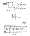
- the two inputs 136 and 138 of the differential amplifier 134 correspondingly drive the amplifier to provide an output respectively at its output lines 140 and 142 to the super buffer 144.
- the first inverter stage of buffer 144 puts the complement of the signal inputs 140 and 142 onto inverter 146 which provides output for the two super buffer stages 148 and 150.
- the output of buffer 144 is an nMOS converted signal, DATA, on line 106.
- the inverter 156 and pass transistor 158 represent a current source 160 for differential amplifier 134.
- the bias circuit 152 and current source 160 provide for the proper functioning of differential amplifier 134.
- the voltage bias circuit 152 ensures that the bias point between the resistors 130 and 132 is high enough to operate the input enhancement transistors of the amplifier 134 and the current source ensures that the voltage drop across the amplifier transistors is sufficient to ensure a high level signal on output lines 140 and 142 to buffer 144.
- the voltage OFFSET is applied to amplifier 134 producing an output high or "1" on line 106. This is exemplified in Figure 10 at input signal for DATA before transition 116 or after end of packet transition 118.
- the data and clock recovery logic 108 comprises conventional logic circuitry to provide (1) for recovery of the data from the input DATA in the form of a non-return to zero (NRZ) signal, which is DATA(NRZ), (2) for providing an indication when data is valid, i.e., when there is data present, or not valid, which is DATA VALID and (3) a receive clock recovery from the input DATA, which is CLOCK.
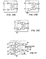
- Figure 12 discloses an implementation for logic 108.
- the incoming data packet on line 106 is supplied to both the non-inverting and inverting inputs of a D flip-flop 170, which has its Q and Q bar outputs connected to D andD bar inputs of another D flip-flop 172.
- the logic for these flip-flops is conventional and disclosed in Figure 13C.
- the CLK input for flip-flop 170 is the 0 ns tap of delay line 101 (see Figure 9).
- the CLK input for flip-flop 172 is the 25 ns tap of delay line 101.
- Incoming signal DATA on line 106 is also supplied to both an inverting and non-inverting input of D flip-flops 174 and 176.
- the Q and Q bar outputs of flip-flop 174 are two inputs 175 and 177 of four inputs to XOR Gate 180.
- the Q an Q bar outputs of flip-flop 176 are connected as inputs of corresponding D flip-flop 178.
- the Q and Q bar outputs of flip-flop 178 are the other two inputs 179 and 181 to XOR gate 180.
- the outputs 183 and 185 to XOR gate 180 are respective inputs to D flip-flop 182.
- the logic configuration for the D type flip-flops 174, 176, 178 and 182 is shown in Figure 13C and is conventional.
- Flip-flop 176 has a CLK input from the 50 ns tap of delay line 101
- flip-flops 174 and 178 have a CLK input from the 100 ns tap of delay line 101
- flip-flop 182 has a CLK input from the 125 ns tap of delay line 101.
- the received clock recovery, DATA CLOCK is provided by an R-S flip-flop 186 with inputs R bar and S bar are connected respectively to the 125 ns and 75 ns tap outputs of delay line 101.
- the logic configuration for this conventional R-S flip-flop is shown in Figure 13A.
- a representation of this clock output for the example shown in Figure 10 is the waveform, DATA CLOCK.
Landscapes
- Engineering & Computer Science (AREA)
- Computer Networks & Wireless Communication (AREA)
- Signal Processing (AREA)
- Physics & Mathematics (AREA)
- Spectroscopy & Molecular Physics (AREA)
- Synchronisation In Digital Transmission Systems (AREA)
- Small-Scale Networks (AREA)
Claims (8)
Applications Claiming Priority (2)
| Application Number | Priority Date | Filing Date | Title |
|---|---|---|---|
| US412637 | 1982-08-30 | ||
| US06/412,637 US4513427A (en) | 1982-08-30 | 1982-08-30 | Data and clock recovery system for data communication controller |
Publications (3)
| Publication Number | Publication Date |
|---|---|
| EP0104761A2 EP0104761A2 (de) | 1984-04-04 |
| EP0104761A3 EP0104761A3 (en) | 1985-08-28 |
| EP0104761B1 true EP0104761B1 (de) | 1988-10-05 |
Family
ID=23633784
Family Applications (1)
| Application Number | Title | Priority Date | Filing Date |
|---|---|---|---|
| EP83304859A Expired EP0104761B1 (de) | 1982-08-30 | 1983-08-23 | Daten- und Taktrückgewinnungssystem für Datenübertragungssteuerungseinrichtung |
Country Status (4)
| Country | Link |
|---|---|
| US (1) | US4513427A (de) |
| EP (1) | EP0104761B1 (de) |
| JP (1) | JPS5957545A (de) |
| DE (1) | DE3378179D1 (de) |
Families Citing this family (54)
| Publication number | Priority date | Publication date | Assignee | Title |
|---|---|---|---|---|
| JPS60145745A (ja) * | 1984-01-09 | 1985-08-01 | Nec Corp | バイフェーズ符号クロック抽出回路 |
| US4637037A (en) * | 1984-08-29 | 1987-01-13 | At&T Teletype Corporation | Biphase signal receiver |
| US5051991A (en) * | 1984-10-17 | 1991-09-24 | Ericsson Ge Mobile Communications Inc. | Method and apparatus for efficient digital time delay compensation in compressed bandwidth signal processing |
| FR2597686B1 (fr) * | 1984-11-07 | 1988-12-23 | Inst Nat Rech Inf Automat | Procede et dispositif pour la transmission de messages entre differentes stations, a travers un reseau local a diffusion. |
| GB8501827D0 (en) * | 1985-01-24 | 1986-09-17 | Plessey Co Plc | Clock extraction from coded data streams |
| US4866711A (en) * | 1986-03-04 | 1989-09-12 | Christian Rovsing A/S Af 1984 | Method of multiplex/demultiplex processing of information and equipment for performing the method |
| US4876700A (en) * | 1986-04-16 | 1989-10-24 | E. F. Johnson Company | Data demodulator |
| US4694261A (en) * | 1986-10-29 | 1987-09-15 | International Business Machines Corporation | Integrated high gain voltage controlled oscillator |
| US4805197A (en) * | 1986-12-18 | 1989-02-14 | Lecroy Corporation | Method and apparatus for recovering clock information from a received digital signal and for synchronizing that signal |
| WO1988005236A1 (en) * | 1987-01-05 | 1988-07-14 | Grumman Aerospace Corporation | High speed data-clock synchronization processor |
| US4841551A (en) * | 1987-01-05 | 1989-06-20 | Grumman Aerospace Corporation | High speed data-clock synchronization processor |
| USRE36671E (en) | 1987-02-06 | 2000-04-25 | Seagate Technology, Inc. | Dual channel readback recovery system |
| US4763338A (en) * | 1987-08-20 | 1988-08-09 | Unisys Corporation | Synchronous signal decoder |
| US4833695A (en) * | 1987-09-08 | 1989-05-23 | Tektronix, Inc. | Apparatus for skew compensating signals |
| JP2731151B2 (ja) * | 1987-09-18 | 1998-03-25 | 株式会社東芝 | 位相情報検出回路 |
| US4868569A (en) * | 1987-12-15 | 1989-09-19 | Schlumberger Well Services | Biphase digital look-ahead demodulating method and apparatus |
| US4977582A (en) * | 1988-03-31 | 1990-12-11 | At&T Bell Laboratories | Synchronization of non-continuous digital bit streams |
| GB2230165B (en) * | 1989-03-30 | 1993-09-15 | Plessey Co Plc | High speed asynchronous data interface |
| JPH0756968B2 (ja) * | 1989-06-23 | 1995-06-14 | 日本電気株式会社 | 多重スタッフ処理回路 |
| US5023891A (en) * | 1989-07-25 | 1991-06-11 | Sf2 Corporation | Method and circuit for decoding a Manchester code signal |
| US4992790A (en) * | 1989-09-19 | 1991-02-12 | Schlumberger Technology Corporation | Digital phase-locked loop biphase demodulating method and apparatus |
| US5119326A (en) * | 1989-12-06 | 1992-06-02 | Transwitch Corporation | Waveshaping transversal filter and method utilizing the same for data transmission over coaxial cable |
| US5103466A (en) * | 1990-03-26 | 1992-04-07 | Intel Corporation | CMOS digital clock and data recovery circuit |
| US5023892A (en) * | 1990-04-06 | 1991-06-11 | Printer Systems Corporation | System for detecting and correcting signal distortion |
| US5239213A (en) * | 1990-04-30 | 1993-08-24 | Advanced Micro Devices, Inc. | Precision timing control programmable logic device |
| US5157655A (en) * | 1990-10-31 | 1992-10-20 | Transwitch Corp. | Apparatus for generating a ds-3 signal from the data component of an sts-1 payload signal |
| EP0483436A1 (de) * | 1990-10-31 | 1992-05-06 | International Business Machines Corporation | Taktfrequenztester |
| JP2770656B2 (ja) * | 1992-05-11 | 1998-07-02 | ヤマハ株式会社 | 集積回路装置 |
| US5367542A (en) * | 1992-06-19 | 1994-11-22 | Advanced Micro Devices, Inc. | Digital data recovery using delay time rulers |
| AU657634B2 (en) * | 1992-06-29 | 1995-03-16 | Dade International Inc. | High-speed time-multiplexed data transmission system |
| US5412697A (en) * | 1993-01-14 | 1995-05-02 | Apple Computer, Inc. | Delay line separator for data bus |
| US5442664A (en) * | 1993-12-20 | 1995-08-15 | Hewlett-Packard Company | Digitally phase modulated clock inhibiting reduced RF emissions |
| FR2723805B1 (fr) * | 1994-08-18 | 1996-10-25 | Matra Mhs | Detecteur de transition d'un signal logique engendrant une impulsion de duree calibree. |
| US6469493B1 (en) | 1995-08-01 | 2002-10-22 | Teradyne, Inc. | Low cost CMOS tester with edge rate compensation |
| JP3080007B2 (ja) * | 1996-08-28 | 2000-08-21 | 日本電気株式会社 | Pll回路 |
| US6028903A (en) * | 1997-03-31 | 2000-02-22 | Sun Microsystems, Inc. | Delay lock loop with transition recycling for clock recovery of NRZ run-length encoded serial data signals |
| US6073259A (en) * | 1997-08-05 | 2000-06-06 | Teradyne, Inc. | Low cost CMOS tester with high channel density |
| US6597752B1 (en) * | 1999-02-24 | 2003-07-22 | Agere Systems Inc. | Method for detecting a dotting sequence for manchester encoded data in a deep fading environment |
| KR100400225B1 (ko) * | 2001-06-27 | 2003-10-01 | 삼성전자주식회사 | 잡음에 강한 버스트 모드 수신 장치 및 그의 클럭 신호 및데이타 복원 방법 |
| KR100926684B1 (ko) * | 2002-11-15 | 2009-11-17 | 삼성전자주식회사 | 스프레드 스펙트럼 클럭 발생기 |
| US7221727B2 (en) * | 2003-04-01 | 2007-05-22 | Kingston Technology Corp. | All-digital phase modulator/demodulator using multi-phase clocks and digital PLL |
| US6856169B2 (en) * | 2003-05-09 | 2005-02-15 | Rambus, Inc. | Method and apparatus for signal reception using ground termination and/or non-ground termination |
| US6924660B2 (en) | 2003-09-08 | 2005-08-02 | Rambus Inc. | Calibration methods and circuits for optimized on-die termination |
| US6980020B2 (en) * | 2003-12-19 | 2005-12-27 | Rambus Inc. | Calibration methods and circuits for optimized on-die termination |
| US7881409B2 (en) * | 2004-01-22 | 2011-02-01 | The Regents Of The University Of Michigan | Demodulator, chip and method for digitally demodulating an FSK signal |
| US7196567B2 (en) * | 2004-12-20 | 2007-03-27 | Rambus Inc. | Systems and methods for controlling termination resistance values for a plurality of communication channels |
| US7389194B2 (en) | 2005-07-06 | 2008-06-17 | Rambus Inc. | Driver calibration methods and circuits |
| TWI373714B (en) * | 2008-04-02 | 2012-10-01 | Novatek Microelectronics Corp | Electronic device for contention detection of bidirectional bus and related method |
| KR101578253B1 (ko) * | 2008-08-12 | 2015-12-16 | 텔레호낙티에볼라게트 엘엠 에릭슨(피유비엘) | 무선 통신 시스템에서의 니어 컴패니언 모드 |
| US8630382B2 (en) * | 2009-03-27 | 2014-01-14 | Freescale Semiconductor, Inc. | Asynchronous data recovery methods and apparatus |
| US9106400B2 (en) * | 2012-10-23 | 2015-08-11 | Futurewei Technologies, Inc. | Hybrid timing recovery for burst mode receiver in passive optical networks |
| US9547333B2 (en) | 2013-10-10 | 2017-01-17 | General Electric Company | System and method for synchronizing networked components |
| CN109891843B (zh) * | 2016-09-08 | 2022-03-08 | 美国莱迪思半导体公司 | 计算机实现的方法和执行计算机实现的方法的系统 |
| FR3068193A1 (fr) | 2017-06-23 | 2018-12-28 | Stmicroelectronics (Grenoble 2) Sas | Dispositif de synchronisation d'horloge |
Family Cites Families (12)
| Publication number | Priority date | Publication date | Assignee | Title |
|---|---|---|---|---|
| JPS5338154B2 (de) * | 1973-08-24 | 1978-10-13 | ||
| US3996481A (en) * | 1974-11-19 | 1976-12-07 | International Business Machines Corporation | FET load gate compensator |
| US4063220A (en) * | 1975-03-31 | 1977-12-13 | Xerox Corporation | Multipoint data communication system with collision detection |
| US3953674A (en) * | 1975-04-04 | 1976-04-27 | Nasa | Telemetry Synchronizer |
| US4103251A (en) * | 1977-05-05 | 1978-07-25 | The United States Of America As Represented By The Secretary Of The Navy | Stabilized delay line oscillator |
| US4185273A (en) * | 1977-07-27 | 1980-01-22 | The United States Of America As Represented By The Secretary Of The Navy | Data rate adaptive control device for Manchester code decoders |
| US4358741A (en) * | 1979-09-17 | 1982-11-09 | Ilc Data Device Corporation | Micro time and phase stepper |
| US4287596A (en) * | 1979-11-26 | 1981-09-01 | Ncr Corporation | Data recovery system for use with a high speed serial link between two subsystems in a data processing system |
| JPS5694654A (en) * | 1979-12-27 | 1981-07-31 | Toshiba Corp | Generating circuit for substrate bias voltage |
| US4282512A (en) * | 1980-02-04 | 1981-08-04 | Xerox Corporation | Data communication system |
| US4363002A (en) * | 1980-11-13 | 1982-12-07 | Fuller Robert M | Clock recovery apparatus for phase shift keyed encoded data |
| US4344041A (en) * | 1981-02-27 | 1982-08-10 | Sperry Corporation | Biphase detector |
-
1982
- 1982-08-30 US US06/412,637 patent/US4513427A/en not_active Expired - Lifetime
-
1983
- 1983-08-23 EP EP83304859A patent/EP0104761B1/de not_active Expired
- 1983-08-23 DE DE8383304859T patent/DE3378179D1/de not_active Expired
- 1983-08-23 JP JP58153987A patent/JPS5957545A/ja active Pending
Also Published As
| Publication number | Publication date |
|---|---|
| US4513427A (en) | 1985-04-23 |
| JPS5957545A (ja) | 1984-04-03 |
| DE3378179D1 (en) | 1988-11-10 |
| EP0104761A2 (de) | 1984-04-04 |
| EP0104761A3 (en) | 1985-08-28 |
Similar Documents
| Publication | Publication Date | Title |
|---|---|---|
| US4513427A (en) | Data and clock recovery system for data communication controller | |
| EP0679307B1 (de) | Verzögerungsleitungsseparator für datenbus | |
| US6031847A (en) | Method and system for deskewing parallel bus channels | |
| EP0112043B1 (de) | Selbsttaktierender binärer Empfänger | |
| JP3720076B2 (ja) | 全二重データ通信のための高速直列リンク | |
| EP0059724B1 (de) | Selbsttaktendes datenübertragungssystem | |
| US6438178B1 (en) | Integrated circuit for receiving a data stream | |
| US6331999B1 (en) | Serial data transceiver architecture and test method for measuring the amount of jitter within a serial data stream | |
| AU618887B2 (en) | High speed asynchronous data interface | |
| US20020064247A1 (en) | Cmos driver and on-chip termination for gigabaud speed data communication | |
| US6949955B2 (en) | Synchronizing signals between clock domains | |
| US7079589B1 (en) | Serial digital communication superimposed on a digital signal over a single wire | |
| US6895062B1 (en) | High speed serial interface | |
| US20210058225A1 (en) | Fast initial phase search for digital clock and data recovery and related systems, devices, and methods | |
| US5365547A (en) | 1X asynchronous data sampling clock for plus minus topology applications | |
| US5748123A (en) | Decoding apparatus for Manchester code | |
| TW200410527A (en) | Multi-port network interface circuit and related method for triggering transmission signals of multiple ports with clocks of different phases | |
| US6996632B2 (en) | Multiphase encoded protocol and synchronization of buses | |
| EP1050138B1 (de) | Cmos treiber und on-chip abschluss für gigabaud schnelle datenkommunikation | |
| US7376211B2 (en) | High speed early/late discrimination systems and methods for clock and data recovery receivers | |
| Bell et al. | A single chip nMOS Ethernet controller | |
| US6987824B1 (en) | Method and system for clock/data recovery for self-clocked high speed interconnects | |
| EP0673139A2 (de) | Wellenformungssender mit Vorkodierung | |
| EP1987644B1 (de) | Datenkommunikationsverfahren sowie Datensende- und -empfangsvorrichtung und -system | |
| US20030123532A1 (en) | Network fabric physical layer |
Legal Events
| Date | Code | Title | Description |
|---|---|---|---|
| PUAI | Public reference made under article 153(3) epc to a published international application that has entered the european phase |
Free format text: ORIGINAL CODE: 0009012 |
|
| AK | Designated contracting states |
Designated state(s): DE FR GB SE |
|
| PUAL | Search report despatched |
Free format text: ORIGINAL CODE: 0009013 |
|
| AK | Designated contracting states |
Designated state(s): DE FR GB SE |
|
| 17P | Request for examination filed |
Effective date: 19860122 |
|
| 17Q | First examination report despatched |
Effective date: 19870317 |
|
| GRAA | (expected) grant |
Free format text: ORIGINAL CODE: 0009210 |
|
| AK | Designated contracting states |
Kind code of ref document: B1 Designated state(s): DE FR GB SE |
|
| ET | Fr: translation filed | ||
| REF | Corresponds to: |
Ref document number: 3378179 Country of ref document: DE Date of ref document: 19881110 |
|
| PLBE | No opposition filed within time limit |
Free format text: ORIGINAL CODE: 0009261 |
|
| STAA | Information on the status of an ep patent application or granted ep patent |
Free format text: STATUS: NO OPPOSITION FILED WITHIN TIME LIMIT |
|
| 26N | No opposition filed | ||
| PGFP | Annual fee paid to national office [announced via postgrant information from national office to epo] |
Ref country code: SE Payment date: 19910612 Year of fee payment: 9 |
|
| PGFP | Annual fee paid to national office [announced via postgrant information from national office to epo] |
Ref country code: FR Payment date: 19910619 Year of fee payment: 9 |
|
| PGFP | Annual fee paid to national office [announced via postgrant information from national office to epo] |
Ref country code: GB Payment date: 19910702 Year of fee payment: 9 |
|
| PGFP | Annual fee paid to national office [announced via postgrant information from national office to epo] |
Ref country code: DE Payment date: 19910830 Year of fee payment: 9 |
|
| PG25 | Lapsed in a contracting state [announced via postgrant information from national office to epo] |
Ref country code: GB Effective date: 19920823 |
|
| PG25 | Lapsed in a contracting state [announced via postgrant information from national office to epo] |
Ref country code: SE Effective date: 19920824 |
|
| GBPC | Gb: european patent ceased through non-payment of renewal fee |
Effective date: 19920823 |
|
| PG25 | Lapsed in a contracting state [announced via postgrant information from national office to epo] |
Ref country code: FR Effective date: 19930430 |
|
| PG25 | Lapsed in a contracting state [announced via postgrant information from national office to epo] |
Ref country code: DE Effective date: 19930501 |
|
| REG | Reference to a national code |
Ref country code: FR Ref legal event code: ST |
|
| EUG | Se: european patent has lapsed |
Ref document number: 83304859.8 Effective date: 19930307 |