EP0100503A2 - Hochfrequentes Multimodefilter mit schmalem Durchlassband - Google Patents
Hochfrequentes Multimodefilter mit schmalem Durchlassband Download PDFInfo
- Publication number
- EP0100503A2 EP0100503A2 EP83107258A EP83107258A EP0100503A2 EP 0100503 A2 EP0100503 A2 EP 0100503A2 EP 83107258 A EP83107258 A EP 83107258A EP 83107258 A EP83107258 A EP 83107258A EP 0100503 A2 EP0100503 A2 EP 0100503A2
- Authority
- EP
- European Patent Office
- Prior art keywords
- filter
- bus bar
- reflectors
- common bus
- electrodes
- Prior art date
- Legal status (The legal status is an assumption and is not a legal conclusion. Google has not performed a legal analysis and makes no representation as to the accuracy of the status listed.)
- Granted
Links
Images


Classifications
-
- H—ELECTRICITY
- H03—ELECTRONIC CIRCUITRY
- H03H—IMPEDANCE NETWORKS, e.g. RESONANT CIRCUITS; RESONATORS
- H03H9/00—Networks comprising electromechanical or electro-acoustic elements; Electromechanical resonators
- H03H9/46—Filters
- H03H9/64—Filters using surface acoustic waves
- H03H9/6423—Means for obtaining a particular transfer characteristic
- H03H9/6433—Coupled resonator filters
-
- H—ELECTRICITY
- H03—ELECTRONIC CIRCUITRY
- H03H—IMPEDANCE NETWORKS, e.g. RESONANT CIRCUITS; RESONATORS
- H03H9/00—Networks comprising electromechanical or electro-acoustic elements; Electromechanical resonators
- H03H9/02—Details
- H03H9/02535—Details of surface acoustic wave devices
- H03H9/02818—Means for compensation or elimination of undesirable effects
- H03H9/02944—Means for compensation or elimination of undesirable effects of ohmic loss
-
- H—ELECTRICITY
- H03—ELECTRONIC CIRCUITRY
- H03H—IMPEDANCE NETWORKS, e.g. RESONANT CIRCUITS; RESONATORS
- H03H9/00—Networks comprising electromechanical or electro-acoustic elements; Electromechanical resonators
- H03H9/46—Filters
- H03H9/64—Filters using surface acoustic waves
- H03H9/6423—Means for obtaining a particular transfer characteristic
- H03H9/6433—Coupled resonator filters
- H03H9/644—Coupled resonator filters having two acoustic tracks
- H03H9/6456—Coupled resonator filters having two acoustic tracks being electrically coupled
- H03H9/6459—Coupled resonator filters having two acoustic tracks being electrically coupled via one connecting electrode
- H03H9/6463—Coupled resonator filters having two acoustic tracks being electrically coupled via one connecting electrode the tracks being electrically cascaded
Definitions
- the present invention relates a high frequency narrow-band multi-mode filter which comprises surface acoustic wave (hereinafter, referred to as SAW) resonators or surface skimming bulk wave (hereinafter, referred to as SSBW) resonators and which exhibits a narrow band pass characteristic of between several tens MHz and 1GHz.
- SAW surface acoustic wave
- SSBW surface skimming bulk wave
- Band pass filters for frequencies above-SOMHz include an LC filter, a spiral filter, a SAW filter or a band pass filter where resonance elements or inductors in a basic circuit are replaced with SAW resonators.
- band pass filters have the following defects.
- the LC and spiral filters have both a low Q value.
- the spiral filter is large in size.
- the SAW filter on the other 20 hand, it has a relatively wide band and a large insertion loss.
- ripples in its pass band due to triple transit'echo (TTE).
- the band width of the filter can be designed with a considerable flexibility, an intermediate stage filter and associated local oscillator in a mobile radio equipment which tends to operate on higher frequencies with crowded frequency allocation can be replaced with the filter of the present invention, whereby the equipment can be effectively made compact, light in weight and inexpensive.
- a common bus bar for SAW or SSBW resonators used in a multi-mode filter is made very narrow and correspondingly the loss of the filter is increased, but the employment of such a structure as will be disclosed later for the bus bar enables the minization of the ohmic loss of the bus bar and thus of the filter loss and also enables the easy connection of the bar to the lead terminals of resonator electrodes.
- a high frequency narrow-band pass multi-mode filter wherein SAW or SSBW resonators are closely disposed to each other on a single piezo-electric substrate to generate different vibration modes of different resonance frequencies, conditions that the resonators are acoustically coupled to each other to cause said vibration modes, are experimentally.found, and said conditions are satisfied by said filter.
- a so-called reflector type multi-mode filter wherein, in order to reduce the ohmic loss of the very narrow common bus bar, the number of strip pairs of electrode in both interdigital transducers (hereinafter referred to as IDT) is minimized and instead reflectors are provided on the both sides of said TDTs to compensate for the reduction of its Q value.
- a part of the bus bar for the IDT electrodes is formed integral with some or all of gratings of the reflectors, whereby the connecting positions of the grating electrodes with respect to lead terminals can be positioned with a high freedom.
- a reflector type multi-mode filter based on SAW or SSBW resonator wherein the common bus bar is extended across gratings of the reflectors so that the width of the bus bar is increased gradually toward both edges of the piezo-electric substrate while the bus bar is connected or not connected to the reflector gratings.
- a reflector type multi-mode filter based on SAW or SSBW resonator wherein electrode lead patterns are provided in place between the IDTs and reflectors, one end of said lead pattern is connected to the common bus bar and the other end is extended to a peripheral edge of the piezo- electric substrate.
- a reflector type multi-mode filter based on SAW or SSBW resonators wherein the common bus bar is extended across grooves of the reflectors up to both edges of the substrate while not connected to the grooves, and the width of the bus bar is increased gradually toward both edges of the piezo-electric substrate.
- the present invention will be detailed on the basis of a theory of estimating parameters determining the acoustic coupling intensity between resonators and of the results of experiments conducted in accordance with the theory.
- the inventors in examining the conditions in which the acoustic coupling is occurred, have estimated the conditions as follows on the basis of the study results of conventional SAW and SSBW resonators.
- two SAW resonators 2 and 3 are disposed on a piezo-electric substrate 1 in a parallel and closely opposed relation so that, when the resonators 2 and 3 are excited and the resultant SAWs are acoustically coupled to each other, the resonators 2 and 3 generate such two vibration modes as shown in Fig. l(b) and (c), that is, symmetrical mode (s-mode) and anti-symmetrical mode (a-mode).
- Fig. 2 shows a vibration mode of a single SAW resonator. It is known that the vibration energy leaks beyond the acoustic aperture of the resonators as illustrated in Fig. 2 and the vibration mode depends on the width w, and thus it will be obvious that the width w is one of the factors determining the acoustic coupling intensity between the both resonators.
- Figs. 3(a) and 3(b) there is qualitatively illustrated a relationship between the vibration mode and the acoustic coupling intensity for the larger and smaller values of g.
- the gap g is a parameter indicative of the adjacency between the both resonators. More specifically, it is considered that, so long as the value q is greater than a certain value, any acoustic coupling will not take place between the resonators 2 and 3 as exaggeratedly depicted in Fig. 3(b), even if the other parameters are in their coupling generation ranges.
- Fig. 5 shows an attenuation characteristic and a relation between the frequencies f and f s .
- an ST cut quartz crystal substrate having a cut angle 37° and a good frequency-temperature characteristic has been employed as the piezo-electric substrate of a filter to be used in the experiments and aluminum electrodes have been formed on a polished main surface of the substrate by the photolithography process.
- the film thicknesses of the electrodes have been selected to be 1.5, 2.2 and 3.0% of the wavelength ⁇ of a surface wave to be excited and the electrode fingers of the upper and lower resonators have been arranged to be the same in phase (that is, to be symmetrical with respect to the common bus bar 6 as shown in Fig. 1).
- the electrode fingers may be arranged not to be symmetrical.
- the number of such electrode finger pairs of IDT has been selected to be 400, 500, 600 and 800 and a center frequency has been selected to be 280MHz.
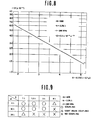
- Fig. 6 is graphs showing an acoustic coupling intensity when the parameter w is fixed and the parameter g is varied
- Fig. 7 is graphs showing an acoustic coupling intensity when the parameter q is fixed and the parameter w is varied.
- the limits of the parameters g and w are about 6X and 20X respectively when the presence or absence of the acoustic coupling is decided on the basis of an impedance characteristic of the filter in which values of w and g were varied.
- the Q value of the resonator becomes very low, which may make it difficult to put the filter to practical use.
- the parameter w is close to 20 ⁇ , the vibration energy is trapped in the acoustic aperture substantially. Accordingly, even if the value g is selected to be small to its manufacturable limit level, the acoustic coupling becomes very weak, which results in a filter having a very narrow pass band width and thus in failure of its practical use.
- the inventors have concluded from the above experimental results that the value w must be selected to be below 20 and the value g must be selected to below 6 ⁇ , desirably below 3 .
- the value g must be set to be extraordinally small when compared with that in the prior art in order that the filter can exhibit its filtering function.
- a narrow band pass filter has a specific band width of between 10 -4 and 10 -3 and thus, if the filter has a center frequency of 280MHz and a band width of 280KHz and the parameter w is set to be 10 ⁇ , then the parameter g has a value of about 10 ⁇ m and the width of the common bus bar 6 is 5 ⁇ m at the largest.
- This bus bar width 5 ⁇ m corresponds to a little less than two times the width (about 2.8 pm) of an IDT electrode finger in a resonator and thus, this means that the common bus bar must be made very narrow, unlike a conventional bus bar in the prior art in which it has been unnecessary to take the ohmic loss of the bus bar into consideration. Since such a narrow bus bar forms an essential requirement to function the SAW double mode filter as a filter, it is necessary to minimize the ohmic loss of the common bus bar to prevent the reduction of the Q value, as will be described later.
- the ST cut quartz crystal substrate having a cut angle of 37° has been used as the piezo-electric substrate.
- the reason why the cut angle of 37° has been chosen is, as well known, for compensating a shift in the peak temperature of the quarts crystal frequency-temperature characteristic caused by mass loading of electrode.
- a quarts crystal substrate having a cut angle of between about 30° and about 43° in the rotated Y-cut system can be used.
- the cut angle of 30° is an angle for shifting the peak temperature of quartz crystal into a room temperature when the aluminum electrode thickness is 5-6% with respect to the wavelength of SAW (spurious will be increased if the electrode thickness exceeds 5-6%)
- the cut angle of 43° is an angle at which the peak temperature of the non-electrode ST cut quartz coincides with a room temperature.
- the cut angle of the quarts crystal substrate When the cut angle of the quarts crystal substrate is used in the above range, the substrate exhibits the most favorable frequency-temperature characteristic, but in manufacturing a. filter, the cut angle is not limited to the above range and other cut angles may be employed according to the specifications of the filter.
- the present invention can be similarly applied to a multiple mode filter based on SSBW resonator.
- SSBW is a wave which propagates immediately below the surface of a piezo-electric substrate and is generated when a rotated Y cut quarts crystal substrate has a cut angle of minus 50° or so and the IDT electrode is attached on the main surface of the substrate to propagate a wave in a Z' direction.
- the pattern of vibration energy trapped in the ITD electrode of the SSBW filter, especially, the energy distribution in the wave propagating direction is exactly the same as that of the SAW resonator.
- the resonator in the filter of the present invention has been of the so-called comb or multiple pair electrode type where multiple pairs of IDT electrodes are employed to obtain a high Q value of the resonator but for the same purpose, the resonator may be of a so-called reflector type where reflectors are disposed on the both sides of IDT electrode.
- this reflector type resonator can have a sufficiently high Q value even if the IDT comprises a relatively small number of electrode fingers pairs, the common bus bar of IDT can be made short and correspondingly the ohmic loss of the bus bar can be decreased and in addition, the characteristic impedance can be designed freely. For these reasons, it is considered, from the view of arranging a filter according to the present invention, that the employment of the reflector type resonator is more preferable than the multiple pair electrode type resonator.
- the reflector type resonator can have a Q value equal to or higher than that of the multiple pair electrode type resonator the number of whose electrode finger corresponds to a total number of the electrode fingers of the IDTs 2 and 3 and the electrode fingers of the reflectors 7 and 8.
- the pitch of the grating of the reflectors 7 and 8 is designed to be slightly wider, (a several hundredth) than that of the IDT, the excited wave can be efficiently reflected.
- the width of the common bus bar 6 must be about 5 ⁇ m at the largest as mentioned earlier and thus it is practically impossible to bond, leading wires on such a narrow bus bar.
- the common bus bar 6 is formed integral with the reflectors 7 and 8 and the IDTs are grounded through the bus bar of the reflectors 7 and 8.
- Fig. 11 shows the electrode pattern of a multi- sectioned double mode filter wherein two of the above-mentioned double mode filter are electrically connected in a tandem manner. More specifically, in the drawing, reflectors 11, 12, 13, and 14 are formed on the both sides of respective double mode resonator filters 9 and 10 on the single substrate 1, the IDT electrodes and reflectors are formed in one shot of photolithography.
- FIG. 12 there is shown yet another embodiment wherein plural pairs of reflectors 16 and 17 are positioned on the both sides of respective IDTs 15 in a multi-staged and adjacent relation.
- the filter arranged as above can provide a high-order shape factor and highly guaranteed attenuations due to the resonance frequency of each mode generated by the acoustic coupling of the vibration energy, and can also provide odd-order shape factor.
- the above double mode filter or the filter comprising multiple stages of said double mode filters can provide only an even-order shape factor.
- each resonator is substituted into respective equivalent constants through Chebyshev characteristic with attenuation peaks.
- Fig. 13 a still further embodiment intended to reduce the above-mentioned ohmic loss of the common bus bar, wherein the common bus bar 6 for a relatively small number of electrode finger pairs in the IDTs 2 and 3 is not connected to the gratings of the reflectors 7 and 8 provided on the both sides of said IDTs 2 and 3 and is extended across the gratings, the width of the common bus bar being gradually increased as the bus bar enters into the reflectors, earthing wires being bonded to the widest ends of the bus bar around the edges of the substrate 1, said wires being connected to ground.
- the length of strips of the gratings is gradually decreased toward outer side of the reflector.
- Such a grating structure might have adverse effect on the propagation and reflection of the excited SAW and thus on the characteristic of the filter, but it has been confirmed from our experiments that such a structure will have no effect on the filter characteristics.
- Fig. 14 shows a modification of the embodiment of Fig. 13, providing the same effect as the embodiment of Fig. 13.
- bus bars 20 and 21 on one sides of the gratings in the reflectors 7 and 8 in Fig. 13 are removed and the above-mentioned tapered common bus bar 6 is extended across the gratings of the reflectors 7 and 8 and connected to the gratings.
- the common bus bar of the electrodes of the IDTs 2 and 3 is symmetrically extended to the one ends of the reflectors on the piezo-electric substrate 1, then the positions of lead terminals 22, passing through a package (not shown), in a air-tight and electrically insulated manner are rotation-symmetrical with respect to the center of the substrate 1, and thus the package can be mounted on a printed circuit board with a high freedom of its mounting direction. Further, since the hot terminals of the electrodes of the IDTs 2 and 3 are separated by the maximum distance, this enables the minimization of the effect on the filter characteristic due to feed through signal.
- FIG. 15 there is shown another embodiment of the present invention, in which lead patterns 23 and 24 are provided between the IDTs 2 or 3 and the reflectors 7 and 8, one ends of the lead patterns 23 and 24 are connected to the common bus bar 6 and the other ends are guided to a peripheral edge of the piezo-electric substrate 1, and the lead patterns 23 and 24 are connected through the guided portions to lead terminals passed through a package of the filter in an electrically isolated manner therefrom.
- bus bars other than the common bus bar 6 are connected to some or all of the gratings of the reflectors 7 or 8, whereby the connecting portions of the strips of the grating connected to lead terminals can be arranged along one side of the substrate 1 and the wire bonding process can be simplified, which results in the fact that the filter with a high reliability can be obtained.
- Fig. 17 is another embodiment of the present invention.
- the common bus bar 6 for a relatively small number of electrode pairs of the IDTs 2 and 3 is extended across the reflectors 7 and 8 provided on the both sides of the IDTs 2 and 3 on the piezo-electric substrate 1, and the width of the common bus bar 6 is gradually increased toward the outer side ends of the reflectors 7 and 8.
- the reflectors 7 and 8 are formed by etching a number of mutually separated grooves 25, and 26 on the substrate 1.
- the filter can exhibit the similar effect.
Landscapes
- Physics & Mathematics (AREA)
- Acoustics & Sound (AREA)
- Surface Acoustic Wave Elements And Circuit Networks Thereof (AREA)
Applications Claiming Priority (2)
| Application Number | Priority Date | Filing Date | Title |
|---|---|---|---|
| JP130140/83 | 1982-07-26 | ||
| JP58130140A JPS5927910A (ja) | 1982-07-16 | 1983-07-15 | 皮膚接触材用ポリマ−とその製造方法 |
Publications (3)
| Publication Number | Publication Date |
|---|---|
| EP0100503A2 true EP0100503A2 (de) | 1984-02-15 |
| EP0100503A3 EP0100503A3 (en) | 1986-02-26 |
| EP0100503B1 EP0100503B1 (de) | 1990-12-12 |
Family
ID=15026916
Family Applications (1)
| Application Number | Title | Priority Date | Filing Date |
|---|---|---|---|
| EP83107258A Expired - Lifetime EP0100503B1 (de) | 1982-07-26 | 1983-07-23 | Hochfrequentes Multimodefilter mit schmalem Durchlassband |
Country Status (1)
| Country | Link |
|---|---|
| EP (1) | EP0100503B1 (de) |
Cited By (5)
| Publication number | Priority date | Publication date | Assignee | Title |
|---|---|---|---|---|
| DE3923209A1 (de) * | 1988-07-20 | 1990-01-25 | Hitachi Ltd | Magnetostatischer bandpassfilter |
| US5077545A (en) * | 1990-05-02 | 1991-12-31 | Sawtek, Inc. | Surface acoustic wave waveguide-coupled resonator notch filter |
| US5374908A (en) * | 1992-11-25 | 1994-12-20 | Rf Monolithics, Inc. | Surface acoustic wave device for generating an output signal with only a symmetric or only an asymmetric vibration mode acoustic wave |
| EP0772293A1 (de) | 1995-11-03 | 1997-05-07 | Micronas Inc. | Elektroakustische Vorrichtung |
| US5793147A (en) * | 1994-05-30 | 1998-08-11 | Murata Manufacturing Co., Ltd. | Surface wave resonator having single component including a plurality of resonant units |
Family Cites Families (2)
| Publication number | Priority date | Publication date | Assignee | Title |
|---|---|---|---|---|
| US4060777A (en) * | 1976-05-19 | 1977-11-29 | Piezo Technology Inc. | Guided elastic surface wave filter |
| JPS5812418A (ja) * | 1981-07-14 | 1983-01-24 | Toyo Commun Equip Co Ltd | 弾性表面波多重モ−ド・フィルタ |
-
1983
- 1983-07-23 EP EP83107258A patent/EP0100503B1/de not_active Expired - Lifetime
Cited By (5)
| Publication number | Priority date | Publication date | Assignee | Title |
|---|---|---|---|---|
| DE3923209A1 (de) * | 1988-07-20 | 1990-01-25 | Hitachi Ltd | Magnetostatischer bandpassfilter |
| US5077545A (en) * | 1990-05-02 | 1991-12-31 | Sawtek, Inc. | Surface acoustic wave waveguide-coupled resonator notch filter |
| US5374908A (en) * | 1992-11-25 | 1994-12-20 | Rf Monolithics, Inc. | Surface acoustic wave device for generating an output signal with only a symmetric or only an asymmetric vibration mode acoustic wave |
| US5793147A (en) * | 1994-05-30 | 1998-08-11 | Murata Manufacturing Co., Ltd. | Surface wave resonator having single component including a plurality of resonant units |
| EP0772293A1 (de) | 1995-11-03 | 1997-05-07 | Micronas Inc. | Elektroakustische Vorrichtung |
Also Published As
| Publication number | Publication date |
|---|---|
| EP0100503A3 (en) | 1986-02-26 |
| EP0100503B1 (de) | 1990-12-12 |
Similar Documents
| Publication | Publication Date | Title |
|---|---|---|
| US4542356A (en) | High frequency narrow-band multi-mode filter | |
| EP0652637B1 (de) | Akustisches Oberflächenwellenfilter | |
| KR100280609B1 (ko) | 탄성표면파필터 | |
| KR100291281B1 (ko) | 탄성표면파장치및이중탄성표면파장치 | |
| KR100290204B1 (ko) | 탄성표면파다중모드필터 | |
| KR100198161B1 (ko) | 탄성 표면파 필터 | |
| USRE33957E (en) | High frequency narrow-band multi-mode filter | |
| KR20030051385A (ko) | 표면탄성파소자 및 그것을 구비한 듀플렉서 | |
| KR20210098344A (ko) | 탄성파 필터 | |
| US12431864B2 (en) | Acoustic wave filter | |
| US5850167A (en) | Surface acoustic wave device | |
| CN118764007B (zh) | 一种弹性波谐振器及弹性波滤波器装置 | |
| EP0100503B1 (de) | Hochfrequentes Multimodefilter mit schmalem Durchlassband | |
| EP0869608B1 (de) | Akustische Oberflächenwellenanordnung | |
| US6335584B1 (en) | Edge reflection type surface acoustic wave device | |
| JPH053169B2 (de) | ||
| EP0763889A1 (de) | Akustisches oberflächenwellenfilter | |
| US6147574A (en) | Unidirectional surface acoustic wave transducer and transversal-type saw filter having the same | |
| US12294353B2 (en) | Acoustic wave element, acoustic wave filter device, and multiplexer | |
| JP2000049558A (ja) | 弾性表面波フィルタ | |
| US6838807B2 (en) | Surface acoustic wave device suitable for use in GHz band | |
| US6781282B1 (en) | Longitudinally coupled resonator-type surface acoustic wave device | |
| JP2002185284A (ja) | 弾性表面波フィルタ | |
| JPH05129884A (ja) | 多段接続多重モードフイルタ | |
| JPH04373304A (ja) | 弾性表面波フィルタ |
Legal Events
| Date | Code | Title | Description |
|---|---|---|---|
| PUAI | Public reference made under article 153(3) epc to a published international application that has entered the european phase |
Free format text: ORIGINAL CODE: 0009012 |
|
| AK | Designated contracting states |
Kind code of ref document: A2 Designated state(s): DE GB |
|
| PUAL | Search report despatched |
Free format text: ORIGINAL CODE: 0009013 |
|
| AK | Designated contracting states |
Kind code of ref document: A3 Designated state(s): DE GB |
|
| 17P | Request for examination filed |
Effective date: 19860612 |
|
| 17Q | First examination report despatched |
Effective date: 19880204 |
|
| GRAA | (expected) grant |
Free format text: ORIGINAL CODE: 0009210 |
|
| AK | Designated contracting states |
Kind code of ref document: B1 Designated state(s): DE GB |
|
| REF | Corresponds to: |
Ref document number: 3382058 Country of ref document: DE Date of ref document: 19910124 |
|
| PLBE | No opposition filed within time limit |
Free format text: ORIGINAL CODE: 0009261 |
|
| STAA | Information on the status of an ep patent application or granted ep patent |
Free format text: STATUS: NO OPPOSITION FILED WITHIN TIME LIMIT |
|
| 26N | No opposition filed | ||
| REG | Reference to a national code |
Ref country code: GB Ref legal event code: 727 |
|
| REG | Reference to a national code |
Ref country code: GB Ref legal event code: 727A Ref country code: GB Ref legal event code: 727 |
|
| REG | Reference to a national code |
Ref country code: GB Ref legal event code: 727B |
|
| REG | Reference to a national code |
Ref country code: GB Ref legal event code: SP |
|
| REG | Reference to a national code |
Ref country code: GB Ref legal event code: IF02 |
|
| PGFP | Annual fee paid to national office [announced via postgrant information from national office to epo] |
Ref country code: GB Payment date: 20020704 Year of fee payment: 20 |
|
| PGFP | Annual fee paid to national office [announced via postgrant information from national office to epo] |
Ref country code: DE Payment date: 20020826 Year of fee payment: 20 |
|
| PG25 | Lapsed in a contracting state [announced via postgrant information from national office to epo] |
Ref country code: GB Free format text: LAPSE BECAUSE OF EXPIRATION OF PROTECTION Effective date: 20030722 |
|
| REG | Reference to a national code |
Ref country code: GB Ref legal event code: PE20 |