EP0100169A2 - Digitales Zeitgetrenntlage-Übertragungssystem - Google Patents
Digitales Zeitgetrenntlage-Übertragungssystem Download PDFInfo
- Publication number
- EP0100169A2 EP0100169A2 EP83303939A EP83303939A EP0100169A2 EP 0100169 A2 EP0100169 A2 EP 0100169A2 EP 83303939 A EP83303939 A EP 83303939A EP 83303939 A EP83303939 A EP 83303939A EP 0100169 A2 EP0100169 A2 EP 0100169A2
- Authority
- EP
- European Patent Office
- Prior art keywords
- bursts
- synchronization
- burst
- frame synchronization
- transmitting
- Prior art date
- Legal status (The legal status is an assumption and is not a legal conclusion. Google has not performed a legal analysis and makes no representation as to the accuracy of the status listed.)
- Withdrawn
Links
Images

Classifications
-
- H—ELECTRICITY
- H04—ELECTRIC COMMUNICATION TECHNIQUE
- H04L—TRANSMISSION OF DIGITAL INFORMATION, e.g. TELEGRAPHIC COMMUNICATION
- H04L5/00—Arrangements affording multiple use of the transmission path
- H04L5/14—Two-way operation using the same type of signal, i.e. duplex
- H04L5/1469—Two-way operation using the same type of signal, i.e. duplex using time-sharing
- H04L5/1484—Two-way operation using the same type of signal, i.e. duplex using time-sharing operating bytewise
- H04L5/1492—Two-way operation using the same type of signal, i.e. duplex using time-sharing operating bytewise with time compression, e.g. operating according to the ping-pong technique
Definitions
- This invention relates to a digital transmission system and is particularly suited for use in a half-duplex system utilizing time compression multiplexing on telephone loops having discontinuities such as cable gauge changes and bridged taps.
- TCM time compression multiplex
- the digital information signal to be transmitted is divided into discrete portions and each portion compressed with respect to time to form a so-called "burst", occupying less than one half the time of the original portion.
- the transmitter at each terminal alternately transmits the burst onto the path, following which the associated receiver at each terminal can receive a corresponding burst from the other transmitter.
- each burst is expanded to occupy its original time span.
- the system appears to be transmitting the two digital information streams continuously and simultaneously i.e. full-duplex communication. So far as the transmission path is concerned, however, half-duplex transmission takes place with alternate bursts travelling in opposite directions.
- each transmitter must wait until the incoming burst from the other transmitter has been cleared from the communication path before it can transmit again. Arrival of the incoming burst will be delayed by at least a time interval equal to twice the transmission delay or propagation time of the path.
- the time interval (dead time) detracts from the efficiency of utilization of the communication path.
- the efficiency decreases as the path length increases.
- the efficiency can be improved, for a given path length, by increasing the length of each burst, thus increasing the "on" time relative to the "dead” time.
- this exacerbates the synchronizing timing problem by increasing the corresponding reception interval during which the receiver is turned off and hence the receiver's clock receives no control bits to keep it synchronized.
- the system also includes circuitry for receiving the bursts of digital signals which includes means for establishing frame synchronization.
- the receiving circuitry also includes gating means responsive to the absence of frame synchronization for passing all received signals to the frame synchronization establishing means; and responsive to the presence of frame synchronization for passing only signals received during a window period which is coextensive with that of said bursts, to the frame synchronization means.
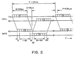
- each received or transmitted burst has a total of 80 information bits (1-80 or 83-162 respectively) preceded and followed by initial and final synchronization bits (0 & 81, or 82 & 163 respectively) for a total of 82 bits per burst.
- All synchronization bits are transmitted as logic 1's while the information bits may be logic 1's or 0's.
- bit period P 6.94 microseconds.
- B 569 microseconds.
- the circuit functions as either a central station or a remote station depending upon the setting of four switches. With the settings illustrated, the circuit will function as a remote station. In addition, there are four possible modes or operating conditions of the circuit which are dependent upon the reception and recognition of the frame synchronization bits in the received digital signal bursts. These operating conditions which are set forth in Table II, control the reception and transmission of the digital signals at the remote station, and the reception only at the central station. This will be manifest together with the detailed structure of the circuit from the following description of its function and operation.
- bursts of digital signals received over a two wire transmission line 2/W are coupled through an input transformer 10 to a receiver 11 where automatic line build out and equalization are carried out in a well-known manner.
- the output of the receiver 11 is connected through an AND-gate 12 which is normally gated open by the output of a NAND-gate 13 during the anticipated period of arrival of the received signal burst.
- the output of the AND-gate 12 is fed to a conventional clock recovery circuit 14 which generates a stable 144Kb/s clock signal at its output. This clock signal is used to drive a 4/9 multiplier 15 which generates a 64Kb/s clock signal at its output.
- the output of the AND-gate 12 is also fed to a buffer 20 which is used to convert the received signal bursts at the 144Kb/s rate to a continuous 64Kb/s digital signal at its output, thereby simulating a full-duplex transmission system at the lower bit rate.
- the 144Kb/s clock signal is also used to clock a 0-179 counter 21 having multiple outputs which are fed to both a receive-decoder 22 and a transmit-decoder 23 to provide gating signals during the designated bit periods of each frame interval in a well-known manner.
- the remote station Prior to the reception of an initial signal burst, the remote station is in a no-sync or searching mode. In this mode, an initially received logic 1 (assumed to be the initial bit of a burst) is gated through an AND-gate 25 to set a D flip-flop 26. A logic 1 at the output of the flip-flop 26 then initializes the output of the counter 21 to 1 to synchronize it to the received digital signal. The logic 1 output of the flip-flop 26 is also used to set a D flip-flop 27 (i.e. samples the occurrence of an initial bit) so that the initial logic 1 synchronization bit of the burst is coupled through an AND-gate 28 to provide an input Qo to a logic circuit 30.
- a D flip-flop 27 i.e. samples the occurrence of an initial bit
- This circuit 30 which comprises four AND-gates, an OR-gate, two D flip-flops and a NOR-gate, functions in a well-known manner to produce the outputs Q 1 and Q 2 whenever the two flip-flops are clocked by the 81st bit period gating pulse from the output of the decoder 22.
- This logic circuit 30 functions in accordance with the truth table shown in Table I. The four possible output combinations of Q 1 and Q 2 determine the conditions detailed in Table II.
- both outputs Q 2 , Q 1 are logic 0's indicating a no-sync or searching condition.
- This output Q 2 is used to gate an AND-gate 31 which in conjunction with the decoder 22 provides an enabling signal to the buffer 20 during reception of bit periods 1-80 (corresponding to the received information signal bit periods) of each frame interval. Thus an output signal from the buffer 20 is obtained only when frame synchronization is confirmed.
- the signal confirming frame synchronization Q 2 together with that from the decoder 22, is also used to gate the NAND-gate 13 so that during subsequent bursts, its output will go to a logic 1 to gate the AND-gate 12 during the bit periods 0-81 of each frame interval.
- the gate 12 is opened only during the anticipated period of reception of the received signal during each frame interval.
- the loss of an isolated synchronization bit does not cause the loss of the signal confirming frame synchronization.
- the loss of alternate synchronization bits, or two or more consecutive synchronization bits will cause the loss of the signal confirming frame synchronization and the circuit to revert to the no-sync or searching mode. It will be evident that due to the widely spaced initial and final synchronization bits, short perturbations of less than 0.5 milliseconds will have no affect on the frame confirmation signal Q 2 , thereby providing an inherent robustness to the system.
- the presence of the synchronization confirmation signal Q 2 also gates an AND-gate 50 which in conjunction with the decoder 23 enables a buffer memory 51 so that the incoming digital information signal at a 64Kb/s rate is converted to bursts of digital signals at the 144Kb/s rate during bit periods 83-162 of each frame interval.
- This transmit information signal is then coupled through an OR-gate 52 where the initial and final synchronization bits occurring in bit periods 82 and 163 are added.
- the combined transmit burst signal at the output of the OR-gate 52 is gated through an AND-gate 53, under control of the synchronization confirmation signal Q 2 , to a line transmitter 54.
- the output of the transmitter 54 is coupled through a transformer 55 to the 2jW telephone loop.
- the operation of the received portion of the circuit is identical to that described with respect to the remote station.
- the transmit portion at the central station operates continuously regardless of whether or not signals are being received from the remote station.
- switches 60, 61, 62, and 63 are switched to their alternate position.
- An internal 64Kb/s clock 65 is then used to clock the input of the buffer 51 and a 9/4 multiplier 66 which generates a 144Kb/s clock signal at its output. This signal is used to clock both the output of the buffer 51 and a 0-179 counter 67.
- the multiple outputs of the counter 67 are in turn connected through switch 62 to the transmit-decoder 23, the outputs of which are coupled to the AND-gate 50 and the OR-gate 52 as described with reference to the remote station.
- gates 50 and 53 are held open by a NOR-gate 68 having a grounded input.
Landscapes
- Engineering & Computer Science (AREA)
- Signal Processing (AREA)
- Computer Networks & Wireless Communication (AREA)
- Time-Division Multiplex Systems (AREA)
- Synchronisation In Digital Transmission Systems (AREA)
- Bidirectional Digital Transmission (AREA)
Applications Claiming Priority (2)
| Application Number | Priority Date | Filing Date | Title |
|---|---|---|---|
| CA408241 | 1982-07-28 | ||
| CA000408241A CA1181183A (en) | 1982-07-28 | 1982-07-28 | Time compression multiplex digital transmission system |
Publications (2)
| Publication Number | Publication Date |
|---|---|
| EP0100169A2 true EP0100169A2 (de) | 1984-02-08 |
| EP0100169A3 EP0100169A3 (de) | 1985-01-09 |
Family
ID=4123298
Family Applications (1)
| Application Number | Title | Priority Date | Filing Date |
|---|---|---|---|
| EP83303939A Withdrawn EP0100169A3 (de) | 1982-07-28 | 1983-07-06 | Digitales Zeitgetrenntlage-Übertragungssystem |
Country Status (3)
| Country | Link |
|---|---|
| EP (1) | EP0100169A3 (de) |
| JP (1) | JPS5943649A (de) |
| CA (1) | CA1181183A (de) |
Cited By (5)
| Publication number | Priority date | Publication date | Assignee | Title |
|---|---|---|---|---|
| EP0100608A3 (en) * | 1982-07-29 | 1985-01-09 | Northern Telecom Limited | Time compression multiplex digital transmission system |
| GB2149513A (en) * | 1983-10-28 | 1985-06-12 | Festo Kg | Proximity sensor |
| WO1985004298A1 (en) * | 1984-03-20 | 1985-09-26 | Applied Spectrum Technologies, Inc. | Data and voice communications system |
| AU588894B2 (en) * | 1985-06-20 | 1989-09-28 | Telefonaktiebolaget Lm Ericsson (Publ) | Arrangement for establishing wide band connection in a switching network |
| DE4125105A1 (de) * | 1991-07-27 | 1993-01-28 | Krone Ag | Bidirektionale datenuebertragung auf einem lichtwellenleiter |
Family Cites Families (4)
| Publication number | Priority date | Publication date | Assignee | Title |
|---|---|---|---|---|
| SE409271B (sv) * | 1977-12-02 | 1979-08-06 | Ellemtel Utvecklings Ab | Sett och anordning for synkronisering av en mottagare vid skurvis overforing medelst ortogonal bifaskod |
| DE2832856A1 (de) * | 1978-07-26 | 1980-02-14 | Siemens Ag | Schaltungsanordnung zum empfang von digitalen nachrichtensignalen in einer digitalen vermittlungsstelle eines zeitmultiplexfernmeldenetzes |
| US4404672A (en) * | 1980-03-28 | 1983-09-13 | Nippon Electric Co., Ltd. | Subscriber terminal for use in a time shared bidirectional digital communication network |
| GB2094106B (en) * | 1981-01-13 | 1984-07-18 | Standard Telephones Cables Ltd | Transmission system |
-
1982
- 1982-07-28 CA CA000408241A patent/CA1181183A/en not_active Expired
-
1983
- 1983-07-06 EP EP83303939A patent/EP0100169A3/de not_active Withdrawn
- 1983-07-28 JP JP13693583A patent/JPS5943649A/ja active Pending
Cited By (6)
| Publication number | Priority date | Publication date | Assignee | Title |
|---|---|---|---|---|
| EP0100608A3 (en) * | 1982-07-29 | 1985-01-09 | Northern Telecom Limited | Time compression multiplex digital transmission system |
| GB2149513A (en) * | 1983-10-28 | 1985-06-12 | Festo Kg | Proximity sensor |
| WO1985004298A1 (en) * | 1984-03-20 | 1985-09-26 | Applied Spectrum Technologies, Inc. | Data and voice communications system |
| US4672605A (en) * | 1984-03-20 | 1987-06-09 | Applied Spectrum Technologies, Inc. | Data and voice communications system |
| AU588894B2 (en) * | 1985-06-20 | 1989-09-28 | Telefonaktiebolaget Lm Ericsson (Publ) | Arrangement for establishing wide band connection in a switching network |
| DE4125105A1 (de) * | 1991-07-27 | 1993-01-28 | Krone Ag | Bidirektionale datenuebertragung auf einem lichtwellenleiter |
Also Published As
| Publication number | Publication date |
|---|---|
| EP0100169A3 (de) | 1985-01-09 |
| CA1181183A (en) | 1985-01-15 |
| JPS5943649A (ja) | 1984-03-10 |
Similar Documents
| Publication | Publication Date | Title |
|---|---|---|
| US4467473A (en) | Time compression multiplex digital transmission system | |
| US4476558A (en) | Time compression multiplex digital transmission system | |
| US4841521A (en) | Method and system for bidirectionally transmitting data | |
| US4644534A (en) | TDMA point-to-multipoint communications system and its use | |
| CA1207390A (en) | Radio telephones having improved transmitting and receiving characteristics | |
| US4637016A (en) | Frame synchronization circuit for digital transmission system | |
| US4502137A (en) | Digital signal transmitting method | |
| EP0042976A1 (de) | Zweirichtungs-Nachrichtensystem für eine digitale Zweidraht-Telefonverbindung | |
| US5020051A (en) | Duplex communications method and system | |
| US4631721A (en) | Bidirectional communication system of a two-wire bus comprising an active terminator | |
| US4404672A (en) | Subscriber terminal for use in a time shared bidirectional digital communication network | |
| US4642805A (en) | Digital link for telephone station sets | |
| EP0100169A2 (de) | Digitales Zeitgetrenntlage-Übertragungssystem | |
| US3651474A (en) | A synchronization system which uses the carrier and bit timing of an adjacent terminal | |
| US4239934A (en) | Means and an apparatus for synchronizing an orthogonal diphase code receiver | |
| US4737722A (en) | Serial port synchronizer | |
| US7372930B2 (en) | Method to synchronize data and a transmitter and a receiver realizing said method | |
| CA1220833A (en) | Frame synchronization circuit for digital transmission system | |
| US4807258A (en) | Method for synchronizing a digital communication system | |
| US3952163A (en) | Method and apparatus for testing in FDM system | |
| SU1443821A3 (ru) | Система синхронизации | |
| JP2718673B2 (ja) | 2線式回線を用いた双方向伝送方法及びその装置 | |
| US3963867A (en) | Method for indicating a free-line state in a binary data communication system | |
| JPS6392135A (ja) | デイジタル加入者線伝送方式 | |
| JPS648941B2 (de) |
Legal Events
| Date | Code | Title | Description |
|---|---|---|---|
| PUAI | Public reference made under article 153(3) epc to a published international application that has entered the european phase |
Free format text: ORIGINAL CODE: 0009012 |
|
| AK | Designated contracting states |
Designated state(s): DE FR GB NL SE |
|
| PUAL | Search report despatched |
Free format text: ORIGINAL CODE: 0009013 |
|
| AK | Designated contracting states |
Designated state(s): DE FR GB NL SE |
|
| STAA | Information on the status of an ep patent application or granted ep patent |
Free format text: STATUS: THE APPLICATION IS DEEMED TO BE WITHDRAWN |
|
| 18D | Application deemed to be withdrawn |
Effective date: 19850910 |
|
| RIN1 | Information on inventor provided before grant (corrected) |
Inventor name: ARNON, EPHRAIM |