EP0100140B1 - Data processing system and method of starting up system - Google Patents
Data processing system and method of starting up system Download PDFInfo
- Publication number
- EP0100140B1 EP0100140B1 EP83303171A EP83303171A EP0100140B1 EP 0100140 B1 EP0100140 B1 EP 0100140B1 EP 83303171 A EP83303171 A EP 83303171A EP 83303171 A EP83303171 A EP 83303171A EP 0100140 B1 EP0100140 B1 EP 0100140B1
- Authority
- EP
- European Patent Office
- Prior art keywords
- microcode
- processor
- program
- main memory
- main
- Prior art date
- Legal status (The legal status is an assumption and is not a legal conclusion. Google has not performed a legal analysis and makes no representation as to the accuracy of the status listed.)
- Expired
Links
Images


Classifications
-
- G—PHYSICS
- G06—COMPUTING; CALCULATING OR COUNTING
- G06F—ELECTRIC DIGITAL DATA PROCESSING
- G06F9/00—Arrangements for program control, e.g. control units
- G06F9/06—Arrangements for program control, e.g. control units using stored programs, i.e. using an internal store of processing equipment to receive or retain programs
- G06F9/44—Arrangements for executing specific programs
- G06F9/4401—Bootstrapping
- G06F9/4403—Processor initialisation
-
- G—PHYSICS
- G06—COMPUTING; CALCULATING OR COUNTING
- G06F—ELECTRIC DIGITAL DATA PROCESSING
- G06F9/00—Arrangements for program control, e.g. control units
- G06F9/06—Arrangements for program control, e.g. control units using stored programs, i.e. using an internal store of processing equipment to receive or retain programs
- G06F9/22—Microcontrol or microprogram arrangements
- G06F9/24—Loading of the microprogram
-
- G—PHYSICS
- G06—COMPUTING; CALCULATING OR COUNTING
- G06F—ELECTRIC DIGITAL DATA PROCESSING
- G06F11/00—Error detection; Error correction; Monitoring
- G06F11/22—Detection or location of defective computer hardware by testing during standby operation or during idle time, e.g. start-up testing
- G06F11/2205—Detection or location of defective computer hardware by testing during standby operation or during idle time, e.g. start-up testing using arrangements specific to the hardware being tested
- G06F11/2236—Detection or location of defective computer hardware by testing during standby operation or during idle time, e.g. start-up testing using arrangements specific to the hardware being tested to test CPU or processors
Description
- This invention relates to a method of starting up a data processing system as set forth in the introductory part of
claim 1 and to a data processing system asset forth in the introductory part ofclaim 16. The invention concerns the loading of the microcode control store, and permits the loading of microcode from a plurality of sources thereof and requires no special controller or specified location for this purpose. - In data processing systems which utilize a control store for storing microcode (i.e. microinstructions) for use in implementing programs in response to the decoding of macroinstructions, for example, the microcode which is loaded therein is usually fixed in nature and only a single set of microcode instructions can be normally so loaded. Such conventional systems, accordingly, tend to be less flexible since they are limited to the loading of only a single set of microinstructions. Moreover, a special controller is normally required in order to access the microcode from an appropriate I/O device (such as a floppy disk, for example) on which the microcode is stored and such controller is normally designed to access only the I/O device which contains the fixed set of microcode instructions. (IBM Technical Disclosure Bulletin Vol. 15,
No 3, Aug 1972, pp 871,872 and DE.OS.1 940 296). - It is desirable, therefore, in order to provide more flexibility to such a microcode system to be able to access more than one set of micro- instructions from more than one I/O device and to do so without the need for one or more special controllers for such purposes associated with each said I/O device.
- It is well known to equip a computer with a small built-in program (bootstrap for loader) which enables the computer to load its basic system software (US 4 117 974) and it is proposed in IBM Technical
Disclosure Bulletin Vol 13,No 3, Aug 1970, p 779 that a central processing unit shall read a bootstrap loaded from selected terminal. The bootstrap loader then permits loading of control programs and data from the terminal into the main memory. - The method and the system according to the present invention are characterised in
claims - In accordance with the invention the system utilises a basic instruction set (often referred to as the "kernel instructions") which can be used to operate the processor and its own normally available internal I/0 controller already part of the system for permitting access to a plurality of I/O devices so at to make available to the microcode control store of the system more than one set of microcode instructions. Such "kernel" micro- instructions may be initially stored in a suitable fixed or programmable read-only-memory (ROM or PROM) and automatically placed in the system's microcode control store at start-up. The "kernel" microinstructions can have associated therewith certain diagnostic microcode instructions which can be used to perform an initial testing of selected basic system components (e.g., a microsequencer unit which controls the sequencing of micro- instructions, an internal instruction processor unit for decoding macroinstructions to provide the starting address of a sequence of micro- instructions in the microcode control store, a main, or subsidary, memory unit, or units, an arithmetic logic unit, etc.).
- The "kernel" microinstructions can then be used to execute a special initialization program which resets the I/O interface units and provides a "start" pulse and a devide code for identifying a particular I/O device in which the desired microcode is stored. Such initialization program accesses a more complex "load" program (a "boot" program) on the previously identified I/O device and transfers such program into the main memory of the system.
- The processor then is able to execute the boot program which searches for the desired microcode file in the identified I/O device (identified by the aforesaid device code) and loads the selected microcode file into the microcode control store of the processor system. Following such loading of the microcode, the processor, now under control of the newly loaded microinstruction set can then load the appropriate operating system software so that the overall system is then ready for use.
- The invention is described in more detail with the help of the accompanying drawings wherein:
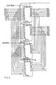
- FIG. 1 depicts a block diagram of pertinent portions of a data processing system in which the invention is used.
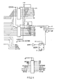
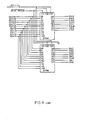
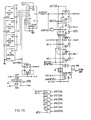
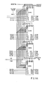
- FIGS. 2 and 2A depict a more detailed logic diagram showing the micro-Nova control processor unit and support logic therefor used in the
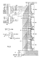
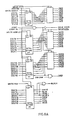
system control processor 11 of FIG. 1; - FIGS. 3, 3A and 3B depict a more detailed logic diagram showing the
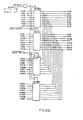
RAM unit 19 of FIG. 1; - FIG. 4 depicts a more detailed logic diagram showing the
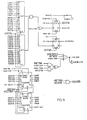
EPROM unit 17 of FIG. 1; - FIG. 5 depicts a more detailed logic diagram of the PROM unit 18 of FIG. 1;
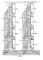
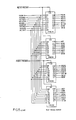
- FIGS. 6, 6A, 6B, 6C and 6D depict a more detailed logic diagram showing internal control logic and internal bus interconnections used in the
system control processor 11 of FIG. 1; - FIGS. 7, 7A and 7B depict a more detailed logic diagram of timing and clock generation logic used in the
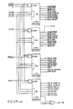
system control processor 11 of FIG. 1; - FIGS. 8, 8A, 8B and 8C depict a more detailed logic diagram of interface logic used in the system control processor of FIG. 1 to interface the
main memory 14 viabus 21; - FIGS. 9 and 9A depict a more detailed logic diagram of interface logic used in the
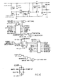
system control processor 11 to interface the microcontrol store via bus 20; and - FIGS. 10 and 10A depict a more detailed logic diagram of the power-up logic used to start operation of the system control processor of FIG. 1.
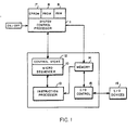
- FIG. 1 shows in broad block diagram form key components of a data processing system which, for example, may be of the type now sold, for example, by Data General Corporation under the designation Eclipse@MV/8000 computer system, as described, for example, in the following document:
- "The Eclipse@MV/8000 Principles of Operation" No. 014-000648, Data General Corporation 1980, (Rev. 01, June 1981). Such system is also described, for example, in our published European application No.
EP 0 039 227. - As can be seen in such above documents the system includes a
microsequencer unit 10 which is used to control the sequential selection of microcode instructions from amicrocode control store 12. Such system is normally under the control of aninstruction processor unit 13 which decodes macroinstructions to provide the starting address in the control store of a sequence of one or more microinstructions required to execute the macroinstruction. The system as shown has an appropriatemain memory system 14 and an I/Ocontroller interface unit 15 which controls the transfer of address and data between the processor and one or more I/O devices 16. - In a particular embodiment of the system in accordance with the invention, such system has, in addition, a
system control processor 11 which is used during the start-up and microcode control store loading operations and which essentially involves specially designed hard-wired logic for accessingPROM units 17 and 18 and a random access memory (RAM)unit 19 and for transferring data betweenmain memory 14 and the control store ofmicrosequencer unit 10. - The system control processor (often hereinafter referred to as the SCP) is initiated upon actuation of the power ON/
OFF switch 21, as diagrammatically shown in FIG. 1. The EPROMunit 17, for example, has a "kernel" microcode instruction set fixedly stored therein. In the particular Data General Eclipse@ MV/8000 system in which the invention can be found useful, for example, such "kernel" microcode instruction set is identified as the Data General Nova° Instruction Set originally designed for use in Data General Corporation's Model Nova@ 800 computer system, as described in the following document: - Programmer's Reference Manual
- Nova Line Computers
- Data General Corporation
- No. 014-000631
- Such "kernel" instruction set is also included as part of the overall instruction set for the Eclipse@ MV/8000 system as described in the previously identified Eclipse@ document. The PROM unit 18 is utilized to store both an initialization program (hereinafter referred to as the "BOOT" program) and a "LOAD CONTROL STORE" (LCS) program, as well as appropriate diagnostic programs for initially testing the system components, as mentioned above. The
RAM unit 19 is available for use in the starting procedures and for the control store loading process in accordance with the invention. - When system power is turned on, the SCP is automatically programmed to transfer the kernel (NOVA 8000) instructions present in the EPROM 17, into the
microcode control store 12 over bus 20. At the same time the LCS program and the power up diagnostic program are transferred from theEPROM 17 to theRAM 19. Once the "kernel" instruction set is made available in the microcode control store, the SCP is used to control the execution of the power up diagnostic program for testing the various components of the overall system as mentioned above. - The kernel instruction set also includes two additional instructions, the first of which can be identified as an "NCPID" instruction which effectively identifies the processor as an MV/8000 processor and, accordingly, prevents any attempt to load microcode instructions other than those which can be used in a Data General Eclipse@ MV/ 8000 computer system. The second additional instruction is identified as the "Load Control Store" (LCS) instruction, which instruction is discussed in more detail below.
- Once the overall "kernel" instruction set (the basic Nova@ 800 instruction set, the NCPID instruction and the LCS instruction) is loaded into the
control store 12, and the diagnostic instructions have been both loaded and executed, the system control processor then transfers the special initialization program (the "BOOT" Program) from PROM 18 to themain memory system 14 over bus 22 and the system's main processor (shown as instruction processor 13) begins execution thereof. - The BOOT program comprises essentially only three macroinstruction steps as follows (the locations represent exemplary locations in the main memory:

main memory 14 for execution, as well as the desired microcode instructions which are to be eventually loaded into themicrocode control store 12 by the aforesaid load control store (LCS) program under control of the MBOOT program. - While the main processor, using the BOOT program, is locating and transferring the MBOOT program from the particular identified I/O device to the
main memory 14, the "JMP" step of the BOOT program prevents the processor from performing any other function until the MBOOT program has been so loaded. Once the MBOOT program is loaded into memory it overrides the JMP step of the BOOT program and the execution of "MBOOT" begins. - The function of the MBOOT program is to search the storage file structure of the identified 1/0 device in order to locate the desired microcode instruction file which isto be loaded into the
microcode control store 12. Thus the MBOOT program is arranged to permit the user to identify a particular microcode file which it desires to be so loaded. Accordingly, as part of the MBOOT program, the user must identify the request file by name, e.g., "MICROCODE". - Once the appropriate microcode file is identified by the MBOOT program, the MBOOT program locates the file in the selected I/O device and transfers up to 16K words of the selected microcode file from the device into the
main memory system 14. - Once the MBOOT program has loaded the first portion fo the selected microcode file into main memory, the "kernel" instruction set then is utilized by the MBOOT program to execute the LCS instruction. This in turn transfers control to the LCS program, this program being executed by the system control processor (SCP) 11. Under such conditions the normally used main instruction processor (which at this stage still operates, in effect, as a Nova 800 processor) is halted and the SCP takes over control of system operation by executing the LCS program, which in the embodiment discussed is stored in
RAM 19. - The microcode instructions exist in main memory in a specifically designated format which can be identified as the MC format. Such microfiche is identified under the title "MC FORMAT". The microcode instructions can then be transferred from the main memory to the after conversion into a form acceptable to the control store. Thus, for example, the first portion of the microcode contains a version of the "kernel" microcode instruction which has originally been loaded into main memory in MC format. Such first portion must then be loaded into the control store in a version which is identical to the original version in operating characteristics but which is modified in both location and content for integrated operation with the entire Eclipse@ MV/8000 instruction set. The remaining portions of the selected microcode file contain the remainder of the MV/8000 instruction set to form the overall instruction set.
- In accordance with both the LCS program, executed by the SCP, and the MC format interpretation of the microcode in main memory, the SCP loads the first portion of the selected microcode instructions from the
main memory 14 into themicrocode control store 12. It then verifies that such first portion was correctly loaded, using well known verification techniques. The SCP then terminates the LCS program, returning control to the MV/8000 main processor which, still functioning as a Nova° 800 processor and still executing the MBOOT program, determines if there is additional microcode to be read from the 1/0 device into main memory. When additional microcode is to be loaded into the control store, the MBOOT program will read the next portion of the selected microcode file intomain memory 14 and issue a subsequent LCS instruction. The subsequent execution of the LCS instruction will cause the same steps of the LCS program which were used by the SCP to load the first portion of microcode into the control store to be performed on this next portion. It should be noted that at this stage the "kernel" instruction set, which is being utilized both to read in further microcode from the 1/0 device and to execute the LCS instruction, has been obtained from the 1/0 device itself. - When all portions of the selected microcode instruction set have been successively transferred, the selected microcode instruction set has been completely loaded into
thecontrol store 12 and the system is then capable of operation as an Eclipse@ MV/8000 processor. Accordingly, the system's normal processor uses the MBOOT program to then load whatever operating system software is required from an appropriate I/O device location via normally available 1/0controller interface unit 15 into themain memory system 14. Once the operating system software has been so loaded, the MBOOT program terminates so that the user can make whatever applications use of the overall system is desired. Since the MV/8000 system is already known to and has been availablefor use by those in the art (as disclosed, for example, in the aforesaid documents) detailed logic diagrams of the normally available components in such system are not necessary. Exemplary logic diagrams therefore have been shown, for example, in the aforesaid Rasala et al U.S. patent application. With reference to the additional components discussed with reference to the invention, detailed logic for thesystem control processor 11, theEPROM 17, the PROM 18 and theRAM 19 are depicted in FIGS. 2-9. Thus, with reference to thesystem control processor 11, the central processor unit and support logic therefore is shown in FIG. 2. internal control logic and bus interconnections are shown in FIG. 6, timing and clock generation is shown in FIG. 7, and power-up logic is shown in FIG. 10. Interface logic for interfacing bus 20 is shown in FIG. 9 and interface logic for interfacingbus 21 is shown in FIG. 8. The RAM unit is shown in FIG. 3, the EPROM unit in FIG. 4 and the PROM unit in Fig. 5.
Claims (23)
Applications Claiming Priority (2)
| Application Number | Priority Date | Filing Date | Title |
|---|---|---|---|
| US06/402,052 US4654783A (en) | 1982-07-26 | 1982-07-26 | Unique process for loading a microcode control store in a data processing system |
| US402052 | 1989-08-31 |
Publications (3)
| Publication Number | Publication Date |
|---|---|
| EP0100140A2 EP0100140A2 (en) | 1984-02-08 |
| EP0100140A3 EP0100140A3 (en) | 1984-07-18 |
| EP0100140B1 true EP0100140B1 (en) | 1987-08-12 |
Family
ID=23590319
Family Applications (1)
| Application Number | Title | Priority Date | Filing Date |
|---|---|---|---|
| EP83303171A Expired EP0100140B1 (en) | 1982-07-26 | 1983-06-02 | Data processing system and method of starting up system |
Country Status (5)
| Country | Link |
|---|---|
| US (1) | US4654783A (en) |
| EP (1) | EP0100140B1 (en) |
| JP (1) | JPS5998251A (en) |
| CA (1) | CA1194604A (en) |
| DE (1) | DE3373032D1 (en) |
Families Citing this family (41)
| Publication number | Priority date | Publication date | Assignee | Title |
|---|---|---|---|---|
| US4720812A (en) * | 1984-05-30 | 1988-01-19 | Racal-Milgo, Inc. | High speed program store with bootstrap |
| JPS6274189A (en) * | 1985-09-27 | 1987-04-04 | Toshiba Corp | Information medium |
| JPH06103460B2 (en) * | 1985-11-19 | 1994-12-14 | ソニー株式会社 | Program transfer method |
| FR2604544B1 (en) * | 1986-09-26 | 1990-12-07 | Ricard Claude | METHODS FOR PROGRAMMING AN ELECTRONIC TAXIMETER AND CORRESPONDING ELECTRONIC TAXIMETERS |
| US4914576A (en) * | 1986-12-18 | 1990-04-03 | Bull Hn Information Systems Inc. | Apparatus and method of loading a control store memory of a central subsystem |
| US4777355A (en) * | 1986-12-24 | 1988-10-11 | Mitsubishi Denki Kabushiki Kaisha | IC card and system for checking the functionality thereof |
| GB2201816A (en) * | 1987-02-27 | 1988-09-07 | Mitac Inc | High speed digital processor |
| EP0551934A2 (en) * | 1987-06-05 | 1993-07-21 | Mitsubishi Denki Kabushiki Kaisha | Digital signal processor |
| JPH01118956A (en) * | 1987-10-31 | 1989-05-11 | Sharp Corp | Data processor |
| JPH01248256A (en) * | 1988-03-30 | 1989-10-03 | Toshiba Corp | Input/output control system |
| US5063496A (en) * | 1988-06-01 | 1991-11-05 | International Business Machines Corporation | Signaling attempted transfer to protected entry point bios routine |
| GB8901932D0 (en) * | 1989-01-28 | 1989-03-15 | Int Computers Ltd | Data processing system |
| FR2645989A1 (en) * | 1989-04-17 | 1990-10-19 | Bull Sa | MULTIFUNCTION COUPLER BETWEEN A CENTRAL COMPUTER UNIT AND THE DIFFERENT PERIPHERAL ORGANS OF THE SAME |
| US5142680A (en) * | 1989-04-26 | 1992-08-25 | Sun Microsystems, Inc. | Method for loading an operating system through a network |
| US5210875A (en) * | 1989-08-25 | 1993-05-11 | International Business Machines Corporation | Initial bios load for a personal computer system |
| US5355489A (en) * | 1989-08-25 | 1994-10-11 | International Business Machines Corp. | Bios load for a personal computer system having a removable processor card |
| JP2868543B2 (en) * | 1989-09-25 | 1999-03-10 | 三菱電機株式会社 | Computer equipment |
| US5155844A (en) * | 1990-02-14 | 1992-10-13 | International Business Machines Corporation | Background memory test during system start up |
| US5557799A (en) * | 1990-03-22 | 1996-09-17 | International Business Machines | Computer determination of operating system or data |
| JP2708608B2 (en) * | 1990-05-25 | 1998-02-04 | 富士通株式会社 | Virtual machine IPL processing method |
| EP0532643B1 (en) * | 1990-06-04 | 1998-12-23 | 3Com Corporation | Method for optimizing software for any one of a plurality of variant architectures |
| US5307497A (en) * | 1990-06-25 | 1994-04-26 | International Business Machines Corp. | Disk operating system loadable from read only memory using installable file system interface |
| JPH0792744B2 (en) * | 1990-08-20 | 1995-10-09 | インターナショナル・ビジネス・マシーンズ・コーポレイション | A method of installing multi-level application software on a data processing device. |
| US6131159A (en) * | 1992-05-08 | 2000-10-10 | Paradyne Corporation | System for downloading programs |
| EP0576126A3 (en) * | 1992-06-22 | 1994-01-12 | International Business Machines Corporation | A method and apparatus for providing a modular ABIOS device support layer in a computer system |
| EP0592079A2 (en) * | 1992-09-20 | 1994-04-13 | Sun Microsystems, Inc. | Automated software installation and operating environment configuration on a computer system |
| US6357000B1 (en) * | 1993-01-29 | 2002-03-12 | Microsoft Corporation | Method and system for specified loading of an operating system |
| US6430685B1 (en) * | 1993-02-19 | 2002-08-06 | Apple Computer, Inc. | Method and apparatus for enabling a computer system |
| EP0622731A3 (en) * | 1993-04-26 | 1995-02-15 | Ibm | Boot architecture for microkernel based systems. |
| US5687371A (en) * | 1993-09-27 | 1997-11-11 | Intel Corporation | Selection from a plurality of bus operating speeds for a processor bus interface during processor reset |
| US5592616A (en) * | 1995-06-07 | 1997-01-07 | Dell Usa, Lp | Method for performing efficient memory testing on large memory arrays using test code executed from cache memory |
| GB2304209B (en) * | 1995-08-04 | 2000-03-01 | Motorola Ltd | Processor system and method of starting-up a processor system |
| US6421798B1 (en) | 1999-07-14 | 2002-07-16 | Computer Service Technology, Inc. | Chipset-based memory testing for hot-pluggable memory |
| US6687858B1 (en) | 2000-05-16 | 2004-02-03 | Phillip M. Adams | Software-hardware welding system |
| JP4958201B2 (en) * | 2001-03-30 | 2012-06-20 | ルネサスエレクトロニクス株式会社 | Microcomputer |
| US6691181B2 (en) * | 2001-10-09 | 2004-02-10 | Phillip M. Adams | Programmatic time-gap defect detection apparatus and method |
| US7472207B2 (en) * | 2001-10-09 | 2008-12-30 | Aftg-Tg, L.L.C. | Optimized-incrementing, time-gap defect detection apparatus and method |
| US6842802B2 (en) * | 2001-11-30 | 2005-01-11 | Aftg-Tg, L.L.C. | Programmatic time-gap defect correction apparatus and method |
| US7003656B2 (en) * | 2002-06-13 | 2006-02-21 | Hewlett-Packard Development Company, L.P. | Automatic selection of firmware for a computer that allows a plurality of process types |
| US7206928B2 (en) * | 2003-06-03 | 2007-04-17 | Digi International Inc. | System boot method |
| CN103713920B (en) * | 2011-06-20 | 2017-11-14 | 北京奇虎科技有限公司 | Portable device system starting protection method and apparatus |
Family Cites Families (10)
| Publication number | Priority date | Publication date | Assignee | Title |
|---|---|---|---|---|
| DE1940296C3 (en) * | 1969-08-07 | 1973-11-29 | Ibm Deutschland Gmbh, 7000 Stuttgart | Device in electronic data processing machines for protecting the control program |
| US4024504A (en) * | 1973-12-21 | 1977-05-17 | Burroughs Corporation | Firmware loader for load time binding |
| US4098895A (en) * | 1975-09-30 | 1978-07-04 | Ciba-Geigy Corporation | Triazolylacetanilide compounds and microbicidal compositions |
| IT1052738B (en) * | 1975-12-24 | 1981-07-20 | Cselt Centro Studi Lab Telecom | DEVICE FOR AUTOMATIC LOADING OF THE CENTRAL MEMORY OF ELECTRONIC CALCULATORS |
| JPS52155939A (en) * | 1976-06-21 | 1977-12-24 | Hitachi Ltd | Control system for micro program |
| US4191996A (en) * | 1977-07-22 | 1980-03-04 | Chesley Gilman D | Self-configurable computer and memory system |
| US4276594A (en) * | 1978-01-27 | 1981-06-30 | Gould Inc. Modicon Division | Digital computer with multi-processor capability utilizing intelligent composite memory and input/output modules and method for performing the same |
| US4334307A (en) * | 1979-12-28 | 1982-06-08 | Honeywell Information Systems Inc. | Data processing system with self testing and configuration mapping capability |
| JPS56152024A (en) * | 1980-04-28 | 1981-11-25 | Toshiba Corp | Automatic initial-program loading system |
| US4414669A (en) * | 1981-07-23 | 1983-11-08 | General Electric Company | Self-testing pipeline processors |
-
1982
- 1982-07-26 US US06/402,052 patent/US4654783A/en not_active Expired - Fee Related
-
1983
- 1983-06-02 EP EP83303171A patent/EP0100140B1/en not_active Expired
- 1983-06-02 DE DE8383303171T patent/DE3373032D1/en not_active Expired
- 1983-07-25 CA CA000433134A patent/CA1194604A/en not_active Expired
- 1983-07-26 JP JP58136694A patent/JPS5998251A/en active Granted
Non-Patent Citations (1)
| Title |
|---|
| IBM Technical Disclosure Bulletin, Vol. 13, No. 3, Aug. 1970 P. 779, MC. 10809 MC 10800M, 138-F77-3,5, DS 9437, 1977 pp. 1-14, Motorola * |
Also Published As
| Publication number | Publication date |
|---|---|
| DE3373032D1 (en) | 1987-09-17 |
| EP0100140A2 (en) | 1984-02-08 |
| US4654783A (en) | 1987-03-31 |
| EP0100140A3 (en) | 1984-07-18 |
| JPH0459651B2 (en) | 1992-09-22 |
| CA1194604A (en) | 1985-10-01 |
| JPS5998251A (en) | 1984-06-06 |
Similar Documents
| Publication | Publication Date | Title |
|---|---|---|
| EP0100140B1 (en) | Data processing system and method of starting up system | |
| KR950002945B1 (en) | Apparatus and method for loading a system reference diskette image from a system partition in a personal computer system | |
| US5022077A (en) | Apparatus and method for preventing unauthorized access to BIOS in a personal computer system | |
| US5355498A (en) | Method and apparatus for booting a computer system without loading a device driver into memory | |
| US6804774B1 (en) | Software image transition aid comprising building a disk image based on identified hardware | |
| EP0417888B1 (en) | Loading method and apparatus for computer system | |
| CA2044119C (en) | Disk operating system loadable from read only memory using installable file system interface | |
| US6421776B1 (en) | Data processor having BIOS packing compression/decompression architecture | |
| US20080010446A1 (en) | Portable apparatus supporting multiple operating systems and supporting method therefor | |
| GB2349247A (en) | Recoverable software installation for a computer system | |
| JPH06324849A (en) | Method and system for activation of operating system environment | |
| US7574696B2 (en) | Multiprocessor application interface requiring no utilization of a multiprocessor operating system | |
| US4679138A (en) | Microsequencer in a data processing system using stack storage for controlling the sequencing of microroutines | |
| WO2008048581A1 (en) | A processing device operation initialization system | |
| US5754852A (en) | Apparatus for combining cellular telephone ring signals and PSTN ring signals | |
| JPS59116875A (en) | Ipl method of multiprocessor system | |
| CN112835596B (en) | Method, system, device and storage medium for installing general operating system | |
| JPH09114673A (en) | Device and method for program loading | |
| Neumann | Disk-based program swapping in 8080-based microcomputers | |
| Lawson | Automatic, network-directed operating system software upgrades: A platform-independent approach | |
| JPH0756742A (en) | Computer system and method for attaining degradation operation of the system | |
| JPS63228332A (en) | Control system for executing instruction | |
| JP2003241984A (en) | Method and program for loading a plurality of os | |
| JPS6242254A (en) | Channel initializing system | |
| JPH07219918A (en) | System starting method for parallel computer |
Legal Events
| Date | Code | Title | Description |
|---|---|---|---|
| PUAI | Public reference made under article 153(3) epc to a published international application that has entered the european phase |
Free format text: ORIGINAL CODE: 0009012 |
|
| AK | Designated contracting states |
Designated state(s): DE FR GB NL |
|
| PUAL | Search report despatched |
Free format text: ORIGINAL CODE: 0009013 |
|
| AK | Designated contracting states |
Designated state(s): DE FR GB NL |
|
| 17P | Request for examination filed |
Effective date: 19841221 |
|
| GRAA | (expected) grant |
Free format text: ORIGINAL CODE: 0009210 |
|
| AK | Designated contracting states |
Kind code of ref document: B1 Designated state(s): DE FR GB NL |
|
| REF | Corresponds to: |
Ref document number: 3373032 Country of ref document: DE Date of ref document: 19870917 |
|
| ET | Fr: translation filed | ||
| PLBE | No opposition filed within time limit |
Free format text: ORIGINAL CODE: 0009261 |
|
| STAA | Information on the status of an ep patent application or granted ep patent |
Free format text: STATUS: NO OPPOSITION FILED WITHIN TIME LIMIT |
|
| 26N | No opposition filed | ||
| PGFP | Annual fee paid to national office [announced via postgrant information from national office to epo] |
Ref country code: GB Payment date: 19930426 Year of fee payment: 11 |
|
| PGFP | Annual fee paid to national office [announced via postgrant information from national office to epo] |
Ref country code: FR Payment date: 19930512 Year of fee payment: 11 |
|
| PGFP | Annual fee paid to national office [announced via postgrant information from national office to epo] |
Ref country code: DE Payment date: 19930527 Year of fee payment: 11 |
|
| PGFP | Annual fee paid to national office [announced via postgrant information from national office to epo] |
Ref country code: NL Payment date: 19930630 Year of fee payment: 11 |
|
| PG25 | Lapsed in a contracting state [announced via postgrant information from national office to epo] |
Ref country code: GB Effective date: 19940602 |
|
| PG25 | Lapsed in a contracting state [announced via postgrant information from national office to epo] |
Ref country code: NL Effective date: 19950101 |
|
| GBPC | Gb: european patent ceased through non-payment of renewal fee |
Effective date: 19940602 |
|
| NLV4 | Nl: lapsed or anulled due to non-payment of the annual fee | ||
| PG25 | Lapsed in a contracting state [announced via postgrant information from national office to epo] |
Ref country code: FR Effective date: 19950228 |
|
| PG25 | Lapsed in a contracting state [announced via postgrant information from national office to epo] |
Ref country code: DE Effective date: 19950301 |
|
| REG | Reference to a national code |
Ref country code: FR Ref legal event code: ST |