EP0099768A1 - Convertisseur de tension à régime de travail constant - Google Patents
Convertisseur de tension à régime de travail constant Download PDFInfo
- Publication number
- EP0099768A1 EP0099768A1 EP83401142A EP83401142A EP0099768A1 EP 0099768 A1 EP0099768 A1 EP 0099768A1 EP 83401142 A EP83401142 A EP 83401142A EP 83401142 A EP83401142 A EP 83401142A EP 0099768 A1 EP0099768 A1 EP 0099768A1
- Authority
- EP
- European Patent Office
- Prior art keywords
- voltage
- transistors
- winding
- transformer
- inductance
- Prior art date
- Legal status (The legal status is an assumption and is not a legal conclusion. Google has not performed a legal analysis and makes no representation as to the accuracy of the status listed.)
- Withdrawn
Links
Images

Classifications
-
- H—ELECTRICITY
- H02—GENERATION; CONVERSION OR DISTRIBUTION OF ELECTRIC POWER
- H02M—APPARATUS FOR CONVERSION BETWEEN AC AND AC, BETWEEN AC AND DC, OR BETWEEN DC AND DC, AND FOR USE WITH MAINS OR SIMILAR POWER SUPPLY SYSTEMS; CONVERSION OF DC OR AC INPUT POWER INTO SURGE OUTPUT POWER; CONTROL OR REGULATION THEREOF
- H02M3/00—Conversion of DC power input into DC power output
- H02M3/22—Conversion of DC power input into DC power output with intermediate conversion into AC
- H02M3/24—Conversion of DC power input into DC power output with intermediate conversion into AC by static converters
- H02M3/28—Conversion of DC power input into DC power output with intermediate conversion into AC by static converters using discharge tubes with control electrode or semiconductor devices with control electrode to produce the intermediate AC
- H02M3/325—Conversion of DC power input into DC power output with intermediate conversion into AC by static converters using discharge tubes with control electrode or semiconductor devices with control electrode to produce the intermediate AC using devices of a triode or a transistor type requiring continuous application of a control signal
- H02M3/335—Conversion of DC power input into DC power output with intermediate conversion into AC by static converters using discharge tubes with control electrode or semiconductor devices with control electrode to produce the intermediate AC using devices of a triode or a transistor type requiring continuous application of a control signal using semiconductor devices only
- H02M3/33569—Conversion of DC power input into DC power output with intermediate conversion into AC by static converters using discharge tubes with control electrode or semiconductor devices with control electrode to produce the intermediate AC using devices of a triode or a transistor type requiring continuous application of a control signal using semiconductor devices only having several active switching elements
- H02M3/33571—Half-bridge at primary side of an isolation transformer
-
- Y—GENERAL TAGGING OF NEW TECHNOLOGICAL DEVELOPMENTS; GENERAL TAGGING OF CROSS-SECTIONAL TECHNOLOGIES SPANNING OVER SEVERAL SECTIONS OF THE IPC; TECHNICAL SUBJECTS COVERED BY FORMER USPC CROSS-REFERENCE ART COLLECTIONS [XRACs] AND DIGESTS
- Y02—TECHNOLOGIES OR APPLICATIONS FOR MITIGATION OR ADAPTATION AGAINST CLIMATE CHANGE
- Y02B—CLIMATE CHANGE MITIGATION TECHNOLOGIES RELATED TO BUILDINGS, e.g. HOUSING, HOUSE APPLIANCES OR RELATED END-USER APPLICATIONS
- Y02B70/00—Technologies for an efficient end-user side electric power management and consumption
- Y02B70/10—Technologies improving the efficiency by using switched-mode power supplies [SMPS], i.e. efficient power electronics conversion e.g. power factor correction or reduction of losses in power supplies or efficient standby modes
Definitions
- the object of the present invention is a DC-DC voltage converter with high operational safety produced with great simplicity of implementation. ''
- Auxiliary passive circuits must be provided to assist in the switching of the transistors, whose role is on the one hand the reduction of the losses by switching and on the other hand the limitation of the speed of rise of the tension, so that this one is lower than the voltage V CEO (collector-emitter, open base), when the collector current is canceled.
- V CEO collector-emitter, open base
- Such a converter has the drawback of being sensitive to transient regimes due to load variations especially at the level of the current in the transistors. Indeed, this assembly comprises a transformer whose primary is affected by the variations in current due to the variations in load and which is connected directly to the transistors by the connection at the midpoint. Thus, the safety of the converter is not absolute. Another drawback stems from the complexity of the switching assistance circuits.
- the converter according to the invention overcomes these drawbacks by operating the transistors independently of the variations in the output load and by simplifying the switching assistance circuits compared to the prior art.
- the converter comprising switching assistance circuits characterized in that the primary of the transformer consists of two windings (P 1 , P 2 ) connected by their common end to the transistors via an inductor L 1 in series with a capacitor C 1 the connection point being the emitter of one and the collector of the other and that the other end of the first winding of the primary is connected to the voltage input point E / 2 and that the other end of the second winding is connected to a second inductor L 2 whose end is connected to ground and to the point input at voltage E by two diodes and that the tuning frequency corresponding to the circuit formed by the inductance L 1 and the capacitor C 1 is lower than the switching frequency of the transistors, and that the primary of the transformer consists of two windings (P 1 , P 2 ) connected by their common end to the transistors via an inductor L 1 in series with a capacitor C 1 the connection point being the emitter of one and the collector of the other and that the other end of the first winding of the primary is connected to the voltage input point E
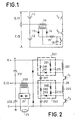
- the general principle of a DC-DC converter is shown in Figure 1.
- the primary of a transformer 10 has its two ends connected on the one hand to two DC voltage sources E / 2, 11 and 12 and on the other share with two switches T 1 and T 2 .
- the switches T 1 and T 2 are closed alternately and periodically so as to obtain at the terminals of the primary a signal in alternating slots of amplitude E / 2.
- the DC output voltage V is obtained at the terminals of the capacitor 16, the value of which depends on the transformation ratio of the transformer 10.
- the switches T 1 and T 2 are generally power transistors or thyristors chosen to support the operating voltages.
- the transistors are made alternately conductive and they operate in switching mode. When a transistor is made conductive, its terminal voltage becomes zero and the current increases; conversely, when a transistor is blocked, its voltage across the terminals increases, while the current becomes zero. In order that the power which it dissipates remains limited and to avoid the transistor being damaged, it is known to use passive "auxiliary switching assistance" circuits.
- FIG. 2 represents a converter according to the prior art.
- the diode bridge and the filter network have been shown diagrammatically by the box 21.
- the switching assistance circuits are constituted for the transistor T 1 by the inductor 221 and a circuit 241 comprising diodes 261 and 271 and the resistors 281 and 291, as well as a capacitor 211.
- the circuit 242 comprising diodes 262 and 272 and the resistors 282 and 292 and the capacitor 212.
- These circuits have a dual role: reduction of switching losses and limitation of the rate of rise of the voltage across the transistors at the time of blocking.
- the capacitors 231 and 232 make it possible to divide the supply voltage by 2 and are designed to support the half-voltage E / 2.
- Such a converter has the disadvantage of being sensitive to transient regimes due to variations in the load, especially at the level of the current in the transistors.
- the primary of the transformer which sees the current variations due to the load variations, is connected directly to the transistors by the connection of the midpoint 26.
- the safety of the converter is not absolute.
- Another drawback stems from the obvious complexity of the switching assistance circuits and from the fact that these circuits include dissipative elements.
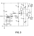
- FIG. 3 represents an exemplary embodiment of the DC-DC converter according to the invention.
- the transformer primary is formed by two windings P 1 and P 21, the second winding P 2 having a number of turns of the order of 10% of the number of turns of P 1 .
- the transistors are connected to the primary of the transformer by a circuit formed by an inductance L 1 and a capacitor C 1 .
- the connection point is located at the common end of P 1 and P 2 , while the winding P 2 is connected at its other end to two diodes D 1 , D 2 via an inductor L 2 .
- a diode D 3 and a capacitor C 2 are placed across the terminals of transistor T 1 as is a diode D 4 and a capacitor C 3 are placed across the terminals of transistor T 2 .
- the circuit L 1 , C 1 is tuned to a frequency lower than the switching frequency of the transistors.
- the transistors T 1 , T 2 are alternately saturated and blocked by the basic currents I B1 and I B2 .
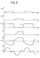
- FIG. 5 shows the corresponding time signals: at the base currents I B1 and I B2 , at the collector-emitter voltage V CE2 of the transistor T 2 , at the collector-emitter current I 2 , at the current I R passing through the winding P 2 and the inductance L 2 at no load I ° R and under load I c R.
- the diode D 4 leads to restore to the power supply the residual energy stored by L 1 during the conduction of T 1 .
- the current in D 4 is canceled and a current I 2 , due to the applied voltage E / 2, appears in the circuit formed by T 2 -D 2 L 2 -P 2 -L 1 -C 1 .
- This current has the shape of a portion of sinusoid and its amplitude is linked to the impedance characteristics of the circuit L 1 - C 1 .
- the voltage V across the winding P 2 remains fixed and is equal to approximately , where N 1 and N 2 are respectively the numbers of turns of the windings P 1 and P 2 .
- the winding P 2 of the transformer is a fixed voltage generator V, whatever the current flowing through it therefore whatever the output load.
- This generator contributes to maintaining the current I 2 and the current in L 1 - C 1 , which is equal to it, constant whether the converter is loaded or empty.
- the current I R in the diodes D 1 and D 2 varies with the load as indicated by the time signals of FIG. 4; it decreases when the load increases and reciprocally.
- the current I R constitutes a current which recovers the variations in current due to the variations in load and contributes to keeping constant the current in the transistors.
- the inductance L 2 is of low value and allows a slight lowering of the current in L 1 - C 1 in the case of no-load operation. Its role is to balance the leakage inductances of P 1 and P 2 (this is a leakage inductance voluntarily added to that of P 2 ). When the recovery current I R decreases, this inductance loses its importance.
- the current flowing in the transistor is absorbed by the capacitors C 2 , C 3 so that to the circuit L 1 - C 1 are added in series the capacitors C 2 and C 3 in parallel , which has the consequence of very significantly increasing the resonant frequency of this circuit (approximately 60 kHz) and allowing the inductance L 1 to discharge much more quickly.
- the current I 2 decreases rapidly while the rise in the voltage V CE2 is slowed down by the capacitors C 2 and C 3 electrically in parallel, as shown by slope 41 of FIG. 4.
- the advantage obtained is a simplification of the switching assistance circuits which no longer comprise, in particular, dissipative elements. The energy is returned to the network instead of being dissipated.
- the basic control of the transistors is carried out by means of 2 transformers providing, with the power transformer, galvanic isolation.
- the rectification in the secondary is carried out by a diode bridge 30 and the filtering is carried out by capacitor at the head, but in reality everything happens as if the equivalent inductance of the circuit L 1 - C 1 , at the frequency considered, was placed in series (to the nearest transformation ratio) in the output circuit.
- the variations in the output voltage are actually those of an overhead inductor filter, which is advantageous for the stability of the value of this voltage as a function of variations in the load.
- this converter comprises a safety device which cuts the basic excitation of the transistors T 1 and T 2 .
- An intensity transformer such as a magnetic toroid 31 is placed so as to provide a voltage proportional to the current flowing in L 1 -C 1 .
- This voltage is rectified but unfiltered to maintain instantaneous operation and compared in a comparison circuit 32 to a fixed threshold voltage. Exceeding this threshold provides a control signal cutting the excitation of the transistors T 1 and T 2 and / or the supply of the voltage E.
- the current flowing in L 1 - C 1 having a strictly constant amplitude , this security is very good.
- the converter operates with four transistors T 1 , T 2 , T 3 and T 4 . These transistors are controlled so that the base currents I B1 and I B4 of the transistors T 1 and T 4 are in phase. It is the same for the base currents I B2 and I B3 of the transistors T 2 and T 3 .
- the primary of the output transformer has three windings P 41 , P 42 and P 43 .
- the utilization circuit 40 includes the secondary of the transformer as well as the load 45.
- the windings P 41 and P 43 correspond to the winding P 2 of FIG. 3 and likewise the inductors L 41 , L42 and L 43 , L 44 correspond to the inductors L 1 and L 2 .
- the diode bridges D 43 , D 44 and D 45 and D 46 having the midpoints A and B are shown.
- the elements for the switching aid C 41 , D 41 are shown for mounting; C 42 , D 42 ; C44, D 47 and C 46 , D 48 for the transistors T 1 , T 2 , T 3 and T 4 respectively .
- a DC-DC converter has been described with a low power used for the switching of the transistors, and having an operation of the transistors independent of the variations in the output load and therefore with a constant thermal regime.
Landscapes
- Engineering & Computer Science (AREA)
- Power Engineering (AREA)
- Dc-Dc Converters (AREA)
Applications Claiming Priority (2)
| Application Number | Priority Date | Filing Date | Title |
|---|---|---|---|
| FR8210242 | 1982-06-11 | ||
| FR8210242A FR2528636A1 (fr) | 1982-06-11 | 1982-06-11 | Convertisseur de tension a regime de travail constant |
Publications (1)
| Publication Number | Publication Date |
|---|---|
| EP0099768A1 true EP0099768A1 (fr) | 1984-02-01 |
Family
ID=9274917
Family Applications (1)
| Application Number | Title | Priority Date | Filing Date |
|---|---|---|---|
| EP83401142A Withdrawn EP0099768A1 (fr) | 1982-06-11 | 1983-06-03 | Convertisseur de tension à régime de travail constant |
Country Status (2)
| Country | Link |
|---|---|
| EP (1) | EP0099768A1 (OSRAM) |
| FR (1) | FR2528636A1 (OSRAM) |
Families Citing this family (2)
| Publication number | Priority date | Publication date | Assignee | Title |
|---|---|---|---|---|
| US4628284A (en) * | 1985-06-03 | 1986-12-09 | North American Philips Corporation | High frequency high voltage power supply preventing simultaneous transistor conduction |
| US4672528A (en) * | 1986-05-27 | 1987-06-09 | General Electric Company | Resonant inverter with improved control |
Citations (6)
| Publication number | Priority date | Publication date | Assignee | Title |
|---|---|---|---|---|
| FR2001712A1 (OSRAM) * | 1968-02-10 | 1969-09-26 | Wandel Et Coltermann | |
| US3947703A (en) * | 1974-10-11 | 1976-03-30 | Compagnie Internationale Pour L'informatique | Regulated supply units |
| DE2613395A1 (de) * | 1976-03-29 | 1977-10-13 | Siemens Ag | Netzgeraet |
| FR2353991A1 (fr) * | 1976-06-01 | 1977-12-30 | Siemens Ag Albis | Convertisseur de tension regle par la tension ou par le courant |
| US4199807A (en) * | 1978-04-24 | 1980-04-22 | Gould Advance Limited | Regulated power supply apparatus |
| GB2070350A (en) * | 1980-02-21 | 1981-09-03 | Chloride Group Ltd | Converters |
-
1982
- 1982-06-11 FR FR8210242A patent/FR2528636A1/fr active Granted
-
1983
- 1983-06-03 EP EP83401142A patent/EP0099768A1/fr not_active Withdrawn
Patent Citations (6)
| Publication number | Priority date | Publication date | Assignee | Title |
|---|---|---|---|---|
| FR2001712A1 (OSRAM) * | 1968-02-10 | 1969-09-26 | Wandel Et Coltermann | |
| US3947703A (en) * | 1974-10-11 | 1976-03-30 | Compagnie Internationale Pour L'informatique | Regulated supply units |
| DE2613395A1 (de) * | 1976-03-29 | 1977-10-13 | Siemens Ag | Netzgeraet |
| FR2353991A1 (fr) * | 1976-06-01 | 1977-12-30 | Siemens Ag Albis | Convertisseur de tension regle par la tension ou par le courant |
| US4199807A (en) * | 1978-04-24 | 1980-04-22 | Gould Advance Limited | Regulated power supply apparatus |
| GB2070350A (en) * | 1980-02-21 | 1981-09-03 | Chloride Group Ltd | Converters |
Also Published As
| Publication number | Publication date |
|---|---|
| FR2528636A1 (fr) | 1983-12-16 |
| FR2528636B1 (OSRAM) | 1985-02-08 |
Similar Documents
| Publication | Publication Date | Title |
|---|---|---|
| KR940007081B1 (ko) | 3권선 초크코일을 구비한 pwm-제어형 전원장치 | |
| FR2738417A1 (fr) | Convertisseur de tension continue a commutation douce | |
| EP0039279A1 (fr) | Interrupteur statique haute tension et utilisation pour un générateur haute tension commutable | |
| FR2627342A1 (fr) | Dispositif d'alimentation de tube luminescent | |
| FR2627644A1 (fr) | Convertisseur continu-continu, sans pertes de commutation, notamment pour alimentation continue haute frequence ou pour amplificateur a tube a ondes progressives | |
| EP1081824A2 (en) | A method and an apparatus for equalising the voltages over the capacitors in a series connection of capacitors during charging and discharging | |
| FR2544139A1 (fr) | Circuit d'alimentation a tres haute tension continue par convertisseur a semi-conducteurs pour les tubes de television notamment | |
| EP0080925A1 (fr) | Convertisseur statique à soupapes électriques comprenant un montage dodécaphase à deux ponts de Graetz pour la suppression des harmoniques 5 et 7 du courant réseau | |
| EP0099768A1 (fr) | Convertisseur de tension à régime de travail constant | |
| EP0443342A1 (fr) | Procédé de contrôle du transfert d'énergie dans un convertisseur statique; convertisseur statique d'énergie pour sa mise en oeuvre et alimentation électrique utilisant un tel convertisseur | |
| EP0002975B1 (fr) | Dispositif de régulation d'une tension continue | |
| EP0184493B1 (fr) | Convertisseur continu-continu à commutateur de découpage et transformateur | |
| EP0176413A1 (fr) | Convertisseur de courant continu en courant continu à découpage | |
| CA2541325A1 (fr) | Convertisseur elevateur de tension | |
| FR2627915A1 (fr) | Convertisseur de puissance de courant continu en courant continu | |
| EP0928057B1 (fr) | Interrupteur haute tension realisé à partir de cellules resonantes connectées en serie | |
| EP0101121B1 (fr) | Dispositifs statiques de conversion d'énergie électrique à semi-conducteurs | |
| FR2550399A1 (fr) | Dispositif d'aide a la commutation | |
| FR2675000A1 (fr) | Procede et dispositif pour attenuer l'effet du radioparasitage par conduction sur le reseau alternatif polyphase. | |
| EP0392420B1 (fr) | Convertisseur continu-continu, à découpage | |
| FR3096188A1 (fr) | Dispositif de sécurité autonome et système électrique comportant un tel dispositif | |
| EP3687051B1 (fr) | Convertisseur resonant serie parallele llcc | |
| FR2578697A2 (fr) | Convertisseur continu/alternatif pour l'alimentation d'un organe utilisateur avec une composante inductive | |
| JP2591889B2 (ja) | 変成器と、保護手段により保護された2つの電子スイッチとを有するシングルエンデッドフォワード方式電力変換器 | |
| EP3270515A1 (fr) | Commutateur ultra-rapide à haute tension |
Legal Events
| Date | Code | Title | Description |
|---|---|---|---|
| PUAI | Public reference made under article 153(3) epc to a published international application that has entered the european phase |
Free format text: ORIGINAL CODE: 0009012 |
|
| AK | Designated contracting states |
Designated state(s): DE GB IT NL SE |
|
| 17P | Request for examination filed |
Effective date: 19840216 |
|
| STAA | Information on the status of an ep patent application or granted ep patent |
Free format text: STATUS: THE APPLICATION HAS BEEN WITHDRAWN |
|
| 18W | Application withdrawn |
Withdrawal date: 19851130 |
|
| RIN1 | Information on inventor provided before grant (corrected) |
Inventor name: GUILLEMIN, GERMAIN |