EP0099724A2 - Aufbringung von Schichten auf Substraten unter Verwendung eines, sich nicht im lokalen thermodynamischen Gleichgewicht befindenden, Hochdruck-Plasmabogens - Google Patents
Aufbringung von Schichten auf Substraten unter Verwendung eines, sich nicht im lokalen thermodynamischen Gleichgewicht befindenden, Hochdruck-Plasmabogens Download PDFInfo
- Publication number
- EP0099724A2 EP0099724A2 EP83304066A EP83304066A EP0099724A2 EP 0099724 A2 EP0099724 A2 EP 0099724A2 EP 83304066 A EP83304066 A EP 83304066A EP 83304066 A EP83304066 A EP 83304066A EP 0099724 A2 EP0099724 A2 EP 0099724A2
- Authority
- EP
- European Patent Office
- Prior art keywords
- arc plasma
- substrate
- plasma
- coating material
- arc
- Prior art date
- Legal status (The legal status is an assumption and is not a legal conclusion. Google has not performed a legal analysis and makes no representation as to the accuracy of the status listed.)
- Withdrawn
Links
Images

Classifications
-
- B—PERFORMING OPERATIONS; TRANSPORTING
- B05—SPRAYING OR ATOMISING IN GENERAL; APPLYING FLUENT MATERIALS TO SURFACES, IN GENERAL
- B05D—PROCESSES FOR APPLYING FLUENT MATERIALS TO SURFACES, IN GENERAL
- B05D1/00—Processes for applying liquids or other fluent materials
-
- C—CHEMISTRY; METALLURGY
- C23—COATING METALLIC MATERIAL; COATING MATERIAL WITH METALLIC MATERIAL; CHEMICAL SURFACE TREATMENT; DIFFUSION TREATMENT OF METALLIC MATERIAL; COATING BY VACUUM EVAPORATION, BY SPUTTERING, BY ION IMPLANTATION OR BY CHEMICAL VAPOUR DEPOSITION, IN GENERAL; INHIBITING CORROSION OF METALLIC MATERIAL OR INCRUSTATION IN GENERAL
- C23C—COATING METALLIC MATERIAL; COATING MATERIAL WITH METALLIC MATERIAL; SURFACE TREATMENT OF METALLIC MATERIAL BY DIFFUSION INTO THE SURFACE, BY CHEMICAL CONVERSION OR SUBSTITUTION; COATING BY VACUUM EVAPORATION, BY SPUTTERING, BY ION IMPLANTATION OR BY CHEMICAL VAPOUR DEPOSITION, IN GENERAL
- C23C14/00—Coating by vacuum evaporation, by sputtering or by ion implantation of the coating forming material
- C23C14/22—Coating by vacuum evaporation, by sputtering or by ion implantation of the coating forming material characterised by the process of coating
- C23C14/24—Vacuum evaporation
- C23C14/32—Vacuum evaporation by explosion; by evaporation and subsequent ionisation of the vapours, e.g. ion-plating
- C23C14/325—Electric arc evaporation
-
- Y—GENERAL TAGGING OF NEW TECHNOLOGICAL DEVELOPMENTS; GENERAL TAGGING OF CROSS-SECTIONAL TECHNOLOGIES SPANNING OVER SEVERAL SECTIONS OF THE IPC; TECHNICAL SUBJECTS COVERED BY FORMER USPC CROSS-REFERENCE ART COLLECTIONS [XRACs] AND DIGESTS
- Y10—TECHNICAL SUBJECTS COVERED BY FORMER USPC
- Y10S—TECHNICAL SUBJECTS COVERED BY FORMER USPC CROSS-REFERENCE ART COLLECTIONS [XRACs] AND DIGESTS
- Y10S376/00—Induced nuclear reactions: processes, systems, and elements
- Y10S376/916—Methods of making fusion fuel targets
Definitions
- This invention relates to the deposition of coatings upon substrates utilising a high pressure, non-local thermal equilibrium arc plasma; more particularly, it relates to the deposition of coatings upon substrates, preferably at atmospheric pressure, by utilising a non-local thermal equilibrium rotating arc plasma.
- Substrates which may be coated include conductive or non-conductive substrates for semiconductor applications and glass microballoons utilised as nuclear fuel targets for inertial confinement fusion processes.
- plasma methods for coating substrates are low pressure processes.
- One method used in the coating of fusion targets is magnetron sputtering either in a batch of bouncing targets or with one target levitated on a gas jet.
- the coating may be damaged or the targets tend to adhere to the bouncing plate or to each other due to either electrostatic interactions or cold welding.
- Levitation processes using gas jets during the coating process are hampered due to the electrostatic interaction between the target and the levitator, while the low pressure required for sputtering hampers the levitation process.
- the deposition of semiconductor materials upon semiconductor substrates has been effected using low pressure deposition processes, such as thermal or plasma assisted chemical vapour deposition or glow discharge, sputtering and thermal evaporation.
- the low pressure plasma deposition processes characteristically exhibit low deposition rates and, where plasma assist is used, low yields of plasma chemical reactions. It is desired, however, to maintain the non-local thermal equilibrium characteristics of the low pressure plasma, which include the existence of free atoms and radicals existing at low temperatures. In non-local thermal equilibrium plasmas, there exist low densities of electrons and molecular species. Additionally, the temperature of the atomic, free radical and molecular species, in ground, ionised or excited states, is much less than the temperature of the electrons.
- U.S. Patent No. 4,003,770 describes a normal plasma spraying process, in which the material is heated with the arc such that molten particles of the coating material are ejected onto the substrate. This is not tailored to allow specific desired chemical reactions to take place, as in the present invention where atomic- sized species of the coating material or materials are activated and these activated species are deposited upon the substrate.
- U.S. Patent No. 4,292,342 describes a high pressure plasma process which utilises a local thermal equilibrium process. Deposition rates using high pressure plasma sources are increased and the yield of plasma chemical processes is greater. However, when utilising high pressure local thermal equilibrium plasmas, there are virtually no activated atomic or free radical species at low gas temperatures. All species including electron, molecular, atomic and radical species, exist at nearly the same temperature. Quenching of the deposition reaction is often necessary and the high temperature involved severely limits the types of deposition materials and chemical interactions which may be utilised.
- a high pressure, non-LTE plasma is generated in an arc and motion of the arc is induced.
- the anode takes the form of a tube and the cathode is a rod in the centre of the tube.
- the arc plasma between the cathode and anode rotates around the interior periphery of the anode, forming a time integrated picture of a rotating disc.
- the residence time of particles in the plasma increases, particularly for those particles which have a high degree of ionisation.
- particles with a low degree of ionisation may also be captured several times in the rotating plasma.
- the temperature distribution of the atomic and radical species in the plasma between the cathode and the periphery of the anode is found to be relatively homogeneous, (although electron temperatures still differ from the temperature of the atomic and radical species), and susceptible for use in the activation of atomic and radical species to permit the smooth coating of substrates.
- the present invention relates to a method'for coating substrates comprising:
- the arc plasma generated is subjected to a magnetic field capable of inducing movement of the arc plasma, most preferably a rotation of the arc in order to produce a more homogeneous temperature distribution and to increase the residence time of species in the plasma.
- coated substrates are prepared by:
- a semiconductor is made by:
- a photovoltaic semiconductor device is made by:
- Electrical conductors may be provided by conventional means to conduct the flow of electricity produced by illuminating the device.
- the device is preferably made with p-type, intrinsic and n-type regions.
- a non-local thermal equilibrium (non-LTE) arc plasma is generated in the presence of a gas between a cathode and an anode of a plasma generating apparatus.
- the gas comprises an inert gas, such as argon, xenon, krypton or helium.
- the gas is introduced into the region of the electrodes at a pressure greater than from 0.1 to 3 atmospheres, preferably at a pressure of approximately 1 atmosphere.
- Coating materials may be introduced into the plasma by several methods.
- the material may be placed on or in the cathode, where it is vaporised by the heat of the cathode and carried into the plasma region by a carrier gas, which may be selected from the gases set forth above.
- the material may be vaporised in the region of the electrodes by an external energy source, such as a laser.
- the material may be volatilised external to the electrode region and transported into the region by the carrier gas, or may be introduced as fine particles in the carrier gas stream.
- the coating materials are introduced into the region of the electrodes in a condensed state, such as a powder, granules, foil or thin wire, and are then volatilised in situ, most conveniently by the heat generated at or on the cathode.
- Coating materials may additionally be introduced into the region of the electrodes in the form of a gas, such as silane, or may be incorporated, if conductive, in a sacrificial cathode.
- Suitable coating materials for deposition upon substrates include silicon and other semiconductor component or dopant materials, including germanium, phosphorus, boron, arsenic, nitrogen, aluminium and gallium, as well as metals, preferably those having a moderate to high ionisation potential, including zinc, copper, nickel, cobalt, iron, cadmium, silver, gold, platinum and palladium.
- silicon and other semiconductor component or dopant materials including germanium, phosphorus, boron, arsenic, nitrogen, aluminium and gallium, as well as metals, preferably those having a moderate to high ionisation potential, including zinc, copper, nickel, cobalt, iron, cadmium, silver, gold, platinum and palladium.
- the choice of coating material selected depends upon the application for which the coated substrate is to be used.
- coated ' substrates may be produced which include semiconductors, photovoltaic thin films, fusion target pellets or coated microballoons, high tolerance bearings and protective coatings, such as passivation layers lSiN 2 ).
- substrates to be utilised may include glass microballoons, quartz, glass, or conductive metals, such as aluminium and stainless steel.
- Semiconductor material may be built up by the deposition process to form at least one discrete layer of one or more materials or elements, in order to conduct electricity.
- this method is suitable for forming photovoltaic thin films of polycrystalline or amorphous material useful in converting radiant energy into electricity.
- a material such as silicon or germanium, may be deposited together with dopant and/or band gap altering elements.
- the types and proportions of the materials introduced into the region of the electrodes may be modified during the deposition process in order that discrete or graded.layers of p, i and n material (as termed in the art) may be successively deposited in a desired order.
- One method of producing inertial fusion targets involves depositing layers of metal around deuterium- tritium, deuterium-deuterium or tritium-tritium fuel containing glass microballoons.
- the metal layers aid in the compression and heating of the nuclear fuel upon being struck by a laser pulse of appropriate energy to cause thermonuclear burn or nuclear fusion of the fuel material.
- a non-LTE arc plasma is generated by impressing a voltage between the cathode and anode in the region of the electrodes causing breakdown of the gas in the electrode region.
- Gas is introduced into the region at a pressure of from 0.1 to 3 atmospheres, preferably about 1 atmosphere or greater.
- the coating material is introduced into the arc plasma as set forth above, preferably being volatilised in the region about the cathode and being carried into the arc plasma by the carrier gas.
- the coating material is excited into activated atomic and radical species by the arc plasma, these activated species being suitable for chemical reaction and deposition onto substrates.
- a substrate is positioned proximate to the arc plasma and the activated species of the coating material which are formed in the plasma are carried by the gas away from the region of the electrodes to contact the substrate and form the coating.
- the arc current utilised to generate the plasma may be as low as 0.5 amps, but is generally from 2 to 10 amps, preferably from 3 to 6 amps.
- the arc current should not exceed amperage which, owing to the nature of the electrode materials utilised, the carrier gases introduced and the coating materials.activated, would cause the arc plasma to lose its substantial non-LTE characteristics. This upper limit amperage may be determined experimentally for a combination of parameters listed.
- the voltage impressed upon the electrodes may be from 20 to 200 volts.
- the magnetic field utilised to induce rotation of the arc plasma may be determined for the particular system utilised by visual observation of that point at which rotation is effected, although field strengths of from 80 to 225 gauss (from 0.008 to 0.0-225 tesla) have been used.
- the temperature of the cathode varies along its length, although temperatures of from 4000 to 6000°C may exist at the tip of the cathode, with temperature rapidly decreasing away from the tip to temperatures of from 500 to 800°C in the area adjacent to the tapered portion of the cathode.
- the temperature of the plasma has been measured on the periphery of the arc at from 200 to 800°C, with temperatures of from 300 to 500°C being preferred.
- the temperature of the plasma jet which emerges from the exit orifice as described below, has been measured at from 200 to,700°C.
- the temperature of the plasma may be increased by increasing the arc current.
- Deposition rates have been measured up to 1 micron (micrometre) per minute on substrates utilising the present invention. This rate represents at least a ten fold increase over conventional low pressure non-LTE deposition processes.
- the rate at which the carrier gas is introduced into the system is dependent upon the temperature at which the plasma is to be operated, the desired residence time for activated species in the plasma and similar considerations, although flow rates of from 1.9 to 3.0 litres argon per minute at atmospheric pressure have been utilised with the apparatus described below.
- an apparatus suitable for carrying out the present invention having a cathode and anode for generating the plasma, means for causing movement of the arc plasma in order to maintain non-LTE conditions, means for introducing the coating materials to the electrode region and regions for positioning substrates permitting deposition of the excited or activated coating material upon the substrates.
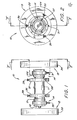
- Figs. 1, 2 and 3 illustrate an apparatus 10 for the deposition of materials upon substrates by means of an arc generated plasma operating under high pressure and non-LTE conditions.
- Apparatus 10 broadly includes anode 11, cathode 12, magnetic field generator 13, environmental control 14 and arc current power supply 15.
- Anode 11 is a cylindrically-shaped hollow electrode, preferably formed of a suitable conductive material, such as graphite or tungsten, capable of withstanding the current and temperature conditions as are known to occur in generating an arc plasma.
- Cathode 12 is a cylindrically-shaped electrode, smaller in diameter than anode 11 and tapered at one end 20, also preferably formed of a suitable conductive material similar to that of anode 11 and most preferably of graphite.
- the tapered end 20 of cathode 12 is extended coaxially within anode 11 by an appropriate mechanism, such as that described below. In this configuration, impression of the necessary voltage and current explained below between anode 11 and cathode 12 will result in an arc being struck between tapered end 20 of cathode 12 and the inner periphery of anode 11 radially closest thereto.
- Environmental control 14 permits selected control of the environment'between anode 11 and cathode 12 necessary for the maintenance of high pressure, non-LTE conditions in the arc plasma and furnishes a vehicle by which the deposition material may be introduced into the arc plasma.
- Environmental control 14 includes two annular end plate housings 21, 22 into which the ends of anode 11 are inserted and two end plates 23, 24 carried respectively in housings 21, 22, all of which together with anode 11 define a closed, hermetically sealed chamber 25 interior to anode 11.
- housings, 21, 22 and end plates 23, 24 must be selected of material, such as ceramics, capable of withstanding the extreme temperatures (typically up to several thousand degrees centigrade) generated during operation of apparatus 10.
- Housings 21, 22 made of ceramics, such as "Lava" material available from 3M Company, South Carolina, U.S.A., and end plates 23, 24 made of sapphire have been found to meet the necessary temperature constraints and permit relatively distortion free viewing of the arc plasma.
- Cathode 12 may pass through a bore 26 in either end plate 23, 24 (for illustration purposes cathode 12 is shown passing through end plate 23) and a gasket 28 interposed between bore 26 and cathode 12 more readily to provide axial support to cathode 12 and maintain chamber 25 hermetically sealed from the ambient environment.
- Gas ports 30, 31 are bored in housings 21, 22, respectively, in order to introduce, exhaust and maintain a preselected gaseous environment at a preselected pressure within chamber 25.
- an arc plasma may be greatly facilitated where the arc plasma is caused to move and most preferably to rotate in a preselected spatial region, maintaining non-LTE characteristics.
- An arc struck and caused to rotate within apparatus 10 between tapered end 20 of cathode 12 and the inner periphery of anode 11 will generate a similarly rotating plasma region which, over time, would define and appear as a disc-shaped region 16.
- Rotation of the plasma arc may be induced by generation of a magentic field having flux lines at right angles to all points along the circular perimeter of anode 11.
- a magentic field having flux lines at right angles to all points along the circular perimeter of anode 11.
- One established technique for furnishing such a magnetic field is the use of a so-called Hemholtz coil arrangement in which two coils 33 and 34 of greater diameter than that of anode 11 are positioned in longitudinal axial alignment with anode 11 radially outward of both ends of chamber 25.
- Upon excitation by a suitable direct current source 35 the requisite stationary magnetic field is established with a highly uniform field magnitude and direction.
- Ring supports 36 and 37 having a plurality of individually adjustable set screws 39 may be provided for support of chamber 25 so that corrections may be made in the alignment of the magnetic field with that of chamber 25.
- apparatus 10 may employ another device or method which would furnish a field, either stationary or time-varient, that would induce the desired motion of the.plasma region. Indeed, dependent upon the specific geometry utilised for material deposition and characteristics of the deposition material, motions other than circular may be preferred for different applications.
- Arc current power supply 15 includes a low voltage (for example, from 30 to 200 volts), low magnitude direct current (for example, from 2 to 10 amperes) power source for electrical connection between anode 11 and cathode 12.
- the exact voltage and current necessary to maintain the arc plasma will be principally dependent upon the ionisation potential of the deposition material and the separation between anode 11 and cathode 12.
- Arc current power supply 15 should be regulated in known manner as fluctuations in current magnitude may adversely affect arc plasma motion. Additionally, power supply 15 may incorporate a high voltage impulse generator, such as a Tesla coil, to furnish the potential required to cause initial breakdown of the gas introduced between anode 11 and cathode 12 and the striking of an arc therebetween.
- a high voltage impulse generator such as a Tesla coil
- a reservoir 40 may be bored in cathode 12 a short distance behind its tapered end 20 and a powdered supply of the desired deposition material placed therein.
- cathode 12 in the vicinity of the reservoir reaches temperatures sufficient to vaporise the deposition material, which is carried into the arc plasma by the carrier gas and activated into states where its atomic species exist in the plasma, which species are then transported by the carrier gas to the deposition site.
- the use of reservoir 40 requires periodic shutdown of apparatus 10 for replenishment of this finite material supply.
- a small bore 41 may be made through the longitudinal axis of cathode 12 and the deposition material 42 continuously fed into chamber 25 therethrough.
- temperatures in the vicinity of tapered end 20 would vaporise the deposition material 42 for introduction into the arc plasma.
- the deposition material may be vaporised within chamber 25 by means for applying heat from an energy source, such as a laser, placed external to chamber 25.
- an energy source such as a laser
- the laser beam utilised could pass through the sapphire end plates 23, 24, which end plates in another embodiment could also provide optical access for still or motion photographic equipment, including real-time video monitors.
- the deposition material may be vaporised externally to apparatus 10 and injected into the carrier gas prior to its entrance into chamber 25. In this instance, however, it may be necessary to preheat the carrier gas and maintain it at an elevated temperature so that the vaporised deposition material does not condense prior to introduction into the arc plasma.
- Deposition may take place in a region either within chamber 25 as best illustrated in Fig. 4, or externally to chamber 25 as illustrated in Figs. 1 and 3.
- a substrate 43 may be interposed between the end of anode 11 and the housing 22, opposite the end plate 23, through which cathode 12 enters chamber 25.
- cathode 12 is extended within chamber 25 until arc plasma region 16 is either adjacent or in spaced apart relation to substrate 43.
- Deposition external of chamber 25 may be effected by inclusion of an exit orifice 44 within anode 11.
- an exit orifice 44 within anode 11.
- Microspheroidal substrates such as glass microballoons, may be removably mounted within chamber 25 by ultilisation of a mounting stalk communicating through a suitable opening in chamber 25.
- substrates may be positioned within chamber 25 or levitated by means of a gas suspension jet or a laser beam (not shown) entering chamber 25.
- arc plasma regions useful for establishing a greater concentration of species of the deposition material in the substrate area, may be established by the insertion of additional cathodes into chamber 25.
- a second cathode (not shown) may be inserted into chamber 25 as illustrated in Figs. 1 and 3 through end plate 24 in the same manner as that of cathode 12.
- Apparatus 10 operates to generate arc plasmas in relatively high pressure (for example, from 0.1 to 3 atmospheres) and exhibiting non-LTE conditions preferable for the deposition of various materials on a variety of substrates, such as quartz, glass or metal, as set forth above.
- a supply of the deposition material for example silicon, other semiconductor dopant or component elements, metals and particularly metals having a moderate to high ionisation potential, is placed in powdered form in reservoir 40 and cathode 12 placed in chamber 25 so that its tapered end 20 is proximate exit orifice 44.
- a carrier gas preferably of an inert element, such as argon, is passed through chamber 25 via gas ports 30 and 31, thereby purging chamber 25 of other gases.
- Active operation is begun by the energisation of coils 33 and 34 with power furnished by direct current source 35 so as to establish the magnetic field by which rotation of the plasma region is induced.
- the Tesla coil in arc current power supply 15 generates a high voltage impulse resulting in an arc being struck between tapered end 20 of cathode 12 and the inner periphery of the anode radially closest thereto.
- arc current power supply 15 impresses across anode 11 and cathode 12 the low voltage, direct current sufficient to maintain the established arc in the preselected gaseous carrier.
- the plasma produced by the arc reaches temperatures of several thousand degrees centigrade.
- the heat produced by the arc is conducted to the cathode, vaporising the metal or other deposition material for transport into the arc plasma for activation into states where its species exist in the plasma.
- the carrier gas further transports these species out exit orifice 44 where anything in that vicinity (such as glass microballoon targets as used in nuclear fusion reactions or flat substrates) may be uniformly coated with the coating material at thickness of from less than one micron (micrometre) to several microns.
- the substrate to be coated could be mounted within anode 11 and cathode 12 appropriately positioned such that the species strike the substrate.
- a quartz substrate was placed into the apparatus as illustrated in Fig. 4, within chamber 25 (interior to anode 11).
- Zinc was introduced to the plasma by.placing granules of zinc metal into reservoir 40 (Fig..3) on the cathode 12.
- the cathode was heated by passage of current, the zinc sublimed and was carried into the plasma by argon carrier gas containing trace amounts of oxygen, introduced at a pressure of about 1 atmosphere at the cathode through gas port 30.
- the quartz substrate was positioned 12 mm from the cathode. An arc was struck by impressing a potential on the electrodes and the rotating plasma was set up by the impression of a magnetic field by the energisation of coils 33 and 34.
- the electrical conductivities of the resulting zinc metal/zinc oxide coatings were found to vary betwen conductive and semjconductive.
- Depositions were conducted with the plasma generating apparauts operating in air, except that argon was introduced into chamber 25 gas ports 30 and 31 and a substrate was placed external to chamber 25 in front of exit orifice 44.
- An arc was struck as in Example 1 and zinc was sublimed from reservoir 40 and cathode 12, carried to the rotating arc plasma 16 where excitation or activation of atomic zinc species occurred.
- the activated zinc coating material was carried by the argon gas through the exit orifice 44 to strike and deposit as zine oxide upon the substrate.
- the arc current utilised was 3 amps and the magentic field was 200 gauss (0.02 tesla).
- Temperature in the jet emitted from the exit orifice was approximately 400°C.
- the substrate was introduced after 7 minutes when the zinc concentration in the plasma had stabilised and was placed 15 mm from the exit orifice.
- Profilometry showed that a coating of approximately 700 nm was obtained in a deposition period of 3 minutes, the coating comprising zinc oxide
- coatings may be achieved utilising non-local thermal equilibrium arc plasmas to generate active species of coating materials.
- Deposition rates are increased greatly over prior art processes which utilise low pressure plasma sources.
- the plasma generating apparatus may be enclosed in a chamber which is filled with an inert gas, such as argon, slightly greater than the pressure at which the deposition is carried out. This prevents oxygen in ambient air from being introduced into the plasma and reacting with the active species generated.
Applications Claiming Priority (2)
| Application Number | Priority Date | Filing Date | Title |
|---|---|---|---|
| US06/398,005 US4505947A (en) | 1982-07-14 | 1982-07-14 | Method for the deposition of coatings upon substrates utilizing a high pressure, non-local thermal equilibrium arc plasma |
| US398005 | 1999-09-16 |
Publications (2)
| Publication Number | Publication Date |
|---|---|
| EP0099724A2 true EP0099724A2 (de) | 1984-02-01 |
| EP0099724A3 EP0099724A3 (de) | 1985-01-23 |
Family
ID=23573600
Family Applications (1)
| Application Number | Title | Priority Date | Filing Date |
|---|---|---|---|
| EP83304066A Withdrawn EP0099724A3 (de) | 1982-07-14 | 1983-07-13 | Aufbringung von Schichten auf Substraten unter Verwendung eines, sich nicht im lokalen thermodynamischen Gleichgewicht befindenden, Hochdruck-Plasmabogens |
Country Status (6)
| Country | Link |
|---|---|
| US (1) | US4505947A (de) |
| EP (1) | EP0099724A3 (de) |
| JP (1) | JPS5931021A (de) |
| KR (1) | KR840005357A (de) |
| CA (1) | CA1196600A (de) |
| IN (1) | IN159621B (de) |
Cited By (3)
| Publication number | Priority date | Publication date | Assignee | Title |
|---|---|---|---|---|
| EP0298157A1 (de) * | 1987-06-29 | 1989-01-11 | Hauzer Holding B.V. | Verfahren und Vorrichtung zur Beschichtung von Aushöhlungen von Gegenständen |
| US5478608A (en) * | 1994-11-14 | 1995-12-26 | Gorokhovsky; Vladimir I. | Arc assisted CVD coating method and apparatus |
| US5587207A (en) * | 1994-11-14 | 1996-12-24 | Gorokhovsky; Vladimir I. | Arc assisted CVD coating and sintering method |
Families Citing this family (32)
| Publication number | Priority date | Publication date | Assignee | Title |
|---|---|---|---|---|
| JPS6110756A (ja) * | 1984-06-25 | 1986-01-18 | Shinei Kk | ガスセンサの製造法 |
| US4929322A (en) * | 1985-09-30 | 1990-05-29 | Union Carbide Corporation | Apparatus and process for arc vapor depositing a coating in an evacuated chamber |
| US4895765A (en) * | 1985-09-30 | 1990-01-23 | Union Carbide Corporation | Titanium nitride and zirconium nitride coating compositions, coated articles and methods of manufacture |
| US4839245A (en) * | 1985-09-30 | 1989-06-13 | Union Carbide Corporation | Zirconium nitride coated article and method for making same |
| US4620913A (en) * | 1985-11-15 | 1986-11-04 | Multi-Arc Vacuum Systems, Inc. | Electric arc vapor deposition method and apparatus |
| US4792460A (en) * | 1986-07-15 | 1988-12-20 | Electric Power Research Institute, Inc. | Method for production of polysilanes and polygermanes, and deposition of hydrogenated amorphous silicon, alloys thereof, or hydrogenated amorphous germanium |
| DE3728420A1 (de) * | 1987-08-26 | 1989-03-09 | Detlev Dipl Phys Dr Repenning | Verfahren zur herstellung von schichten mit hochharten und/oder reibarmen eigenschaften |
| US4898748A (en) * | 1988-08-31 | 1990-02-06 | The Board Of Trustees Of Leland Stanford Junior University | Method for enhancing chemical reactivity in thermal plasma processes |
| US5204144A (en) * | 1991-05-10 | 1993-04-20 | Celestech, Inc. | Method for plasma deposition on apertured substrates |
| US5342660A (en) * | 1991-05-10 | 1994-08-30 | Celestech, Inc. | Method for plasma jet deposition |
| EP0969120B1 (de) * | 1991-05-10 | 2003-07-30 | Celestech, Inc. | Verfahren zur Plasmabeschichtung |
| US5366764A (en) * | 1992-06-15 | 1994-11-22 | Sunthankar Mandar B | Environmentally safe methods and apparatus for depositing and/or reclaiming a metal or semi-conductor material using sublimation |
| WO1995012883A1 (en) * | 1993-11-01 | 1995-05-11 | Eneco, Inc. | Glow discharge apparatus and methods providing prerequisites and testing for nuclear reactions |
| US5830540A (en) * | 1994-09-15 | 1998-11-03 | Eltron Research, Inc. | Method and apparatus for reactive plasma surfacing |
| US5551983A (en) * | 1994-11-01 | 1996-09-03 | Celestech, Inc. | Method and apparatus for depositing a substance with temperature control |
| US5679404A (en) * | 1995-06-07 | 1997-10-21 | Saint-Gobain/Norton Industrial Ceramics Corporation | Method for depositing a substance with temperature control |
| WO1997018074A1 (en) * | 1995-11-13 | 1997-05-22 | General Magnaplate Corporation | Fabrication of tooling by thermal spraying |
| US6173672B1 (en) | 1997-06-06 | 2001-01-16 | Celestech, Inc. | Diamond film deposition on substrate arrays |
| US6406760B1 (en) | 1996-06-10 | 2002-06-18 | Celestech, Inc. | Diamond film deposition on substrate arrays |
| US5952061A (en) * | 1996-12-27 | 1999-09-14 | Stanley Electric Co., Ltd. | Fabrication and method of producing silicon films |
| US6110544A (en) | 1997-06-26 | 2000-08-29 | General Electric Company | Protective coating by high rate arc plasma deposition |
| RU2263006C2 (ru) * | 2000-02-10 | 2005-10-27 | Тетроникс Лимитед | Плазменно-дуговой реактор и способ получения тонких порошков |
| AU2003209606A1 (en) * | 2002-01-14 | 2003-07-24 | Varco Ltd. | Cathode for vacuum arc evaporators |
| JP4014982B2 (ja) * | 2002-09-19 | 2007-11-28 | 株式会社神戸製鋼所 | アーク蒸発源用のロッドターゲット、その製造方法及びアーク蒸着装置 |
| US7504008B2 (en) * | 2004-03-12 | 2009-03-17 | Applied Materials, Inc. | Refurbishment of sputtering targets |
| US7679027B2 (en) * | 2005-03-17 | 2010-03-16 | Far-Tech, Inc. | Soft x-ray laser based on z-pinch compression of rotating plasma |
| US9127362B2 (en) | 2005-10-31 | 2015-09-08 | Applied Materials, Inc. | Process kit and target for substrate processing chamber |
| US8647484B2 (en) * | 2005-11-25 | 2014-02-11 | Applied Materials, Inc. | Target for sputtering chamber |
| US20080023070A1 (en) * | 2006-07-28 | 2008-01-31 | Sanjai Sinha | Methods and systems for manufacturing polycrystalline silicon and silicon-germanium solar cells |
| US8968536B2 (en) * | 2007-06-18 | 2015-03-03 | Applied Materials, Inc. | Sputtering target having increased life and sputtering uniformity |
| US7901552B2 (en) | 2007-10-05 | 2011-03-08 | Applied Materials, Inc. | Sputtering target with grooves and intersecting channels |
| EP2607517A1 (de) * | 2011-12-22 | 2013-06-26 | Oerlikon Trading AG, Trübbach | Niedertemperatur-Lichtbogenionen-Plattierbeschichtung |
Citations (2)
| Publication number | Priority date | Publication date | Assignee | Title |
|---|---|---|---|---|
| US4003770A (en) * | 1975-03-24 | 1977-01-18 | Monsanto Research Corporation | Plasma spraying process for preparing polycrystalline solar cells |
| US4292342A (en) * | 1980-05-09 | 1981-09-29 | Motorola, Inc. | High pressure plasma deposition of silicon |
Family Cites Families (3)
| Publication number | Priority date | Publication date | Assignee | Title |
|---|---|---|---|---|
| US3677807A (en) * | 1969-09-29 | 1972-07-18 | Richard S Curtis | Method of making bearing balls |
| US3925177A (en) * | 1973-01-30 | 1975-12-09 | Boeing Co | Method and apparatus for heating solid and liquid particulate material to vaporize or disassociate the material |
| US4024617A (en) * | 1973-03-06 | 1977-05-24 | Ramsey Corporation | Method of applying a refractory coating to metal substrate |
-
1982
- 1982-07-14 US US06/398,005 patent/US4505947A/en not_active Expired - Fee Related
-
1983
- 1983-06-17 IN IN411/DEL/83A patent/IN159621B/en unknown
- 1983-06-29 CA CA000431392A patent/CA1196600A/en not_active Expired
- 1983-07-12 KR KR1019830003172A patent/KR840005357A/ko not_active Application Discontinuation
- 1983-07-13 EP EP83304066A patent/EP0099724A3/de not_active Withdrawn
- 1983-07-14 JP JP58128701A patent/JPS5931021A/ja active Pending
Patent Citations (2)
| Publication number | Priority date | Publication date | Assignee | Title |
|---|---|---|---|---|
| US4003770A (en) * | 1975-03-24 | 1977-01-18 | Monsanto Research Corporation | Plasma spraying process for preparing polycrystalline solar cells |
| US4292342A (en) * | 1980-05-09 | 1981-09-29 | Motorola, Inc. | High pressure plasma deposition of silicon |
Non-Patent Citations (3)
| Title |
|---|
| AIAA JOURNAL, vol. 10, no. 1, January 1972, pages 17,18, New York, USA; K.J. CLARK et al.: "Thermochemical nonequilibrium in an argon constricted arc plasma" * |
| JOURNAL OF THE ELECTROCHEMICAL SOCIETY, vol. 128, no. 12, December 1981, pages 2647-2655, Manchester, New Hampshire; USA; K.R. SARMA et al.: "High pressure plasma (HPP) deposition of polycrystalline silicon ribbons" * |
| JOURNAL PHYS. D: APPL. PHYS., vol. 8, no. 12, 1975, pages 1423-1425, Letchworth, Herts, GB; J. LOTRIAN et al.: "Etude de l'émission continué d'une décharge d'arc entre electrodes de graphite dans la région 2400-5000 A" * |
Cited By (4)
| Publication number | Priority date | Publication date | Assignee | Title |
|---|---|---|---|---|
| EP0298157A1 (de) * | 1987-06-29 | 1989-01-11 | Hauzer Holding B.V. | Verfahren und Vorrichtung zur Beschichtung von Aushöhlungen von Gegenständen |
| US5026466A (en) * | 1987-06-29 | 1991-06-25 | Hauzer Holding B.V. | Method and device for coating cavities of objects |
| US5478608A (en) * | 1994-11-14 | 1995-12-26 | Gorokhovsky; Vladimir I. | Arc assisted CVD coating method and apparatus |
| US5587207A (en) * | 1994-11-14 | 1996-12-24 | Gorokhovsky; Vladimir I. | Arc assisted CVD coating and sintering method |
Also Published As
| Publication number | Publication date |
|---|---|
| JPS5931021A (ja) | 1984-02-18 |
| CA1196600A (en) | 1985-11-12 |
| EP0099724A3 (de) | 1985-01-23 |
| US4505947A (en) | 1985-03-19 |
| KR840005357A (ko) | 1984-11-12 |
| IN159621B (de) | 1987-05-30 |
Similar Documents
| Publication | Publication Date | Title |
|---|---|---|
| US4505947A (en) | Method for the deposition of coatings upon substrates utilizing a high pressure, non-local thermal equilibrium arc plasma | |
| EP0753081B1 (de) | System zur Elektronstrahlabscheidung aus der Gasphase | |
| US4487162A (en) | Magnetoplasmadynamic apparatus for the separation and deposition of materials | |
| US4980610A (en) | Plasma generators | |
| EP0286306A1 (de) | Verfahren und Vorrichtung zur Gasphasenabscheidung von Diamant | |
| US5441624A (en) | Triggered vacuum anodic arc | |
| US4536640A (en) | High pressure, non-logical thermal equilibrium arc plasma generating apparatus for deposition of coatings upon substrates | |
| US10354845B2 (en) | Atmospheric pressure pulsed arc plasma source and methods of coating therewith | |
| EP0720206A1 (de) | Plasmabehandlungsverfahren und -vorrichtung | |
| RU2455119C2 (ru) | Способ получения наночастиц | |
| AU2002332200B2 (en) | Method for carrying out homogeneous and heterogeneous chemical reactions using plasma | |
| Boxman et al. | Filtered vacuum arc deposition of semiconductor thin films | |
| CA1197493A (en) | High pressure, non-local thermal equilibrium arc plasma generating apparatus for deposition of coating upon substrates | |
| RU2032765C1 (ru) | Способ нанесения алмазного покрытия из паровой фазы и устройство для его осуществления | |
| JPS6250098A (ja) | 金属化合物の粉末冶金装置 | |
| JP2857743B2 (ja) | 薄膜形成装置および薄膜形成方法 | |
| WO2001059175A1 (fr) | Procede de fabrication d'un film conducteur dope nanocomposite de type de diamant et film conducteur dope nanocomposite de type de diamant | |
| WO2000005017A1 (en) | Method and apparatus for producing material vapour | |
| US20070110644A1 (en) | System for manufacturing a fullerene derivative and method for manufacturing | |
| JP3232130B2 (ja) | 薄膜形成装置及びその動作方法 | |
| JPH0775689B2 (ja) | 熱プラズマジェット発生装置 | |
| JPH04120271A (ja) | クラスタイオンビーム発生方法およびクラスタイオンビーム発生装置 | |
| JPH01271A (ja) | マイクロ波プラズマcvd装置 | |
| JPH0764534B2 (ja) | 材料の分離および析出の電磁流体力学的装置および方法 | |
| US4414082A (en) | Process for cracking hydrocarbons |
Legal Events
| Date | Code | Title | Description |
|---|---|---|---|
| PUAI | Public reference made under article 153(3) epc to a published international application that has entered the european phase |
Free format text: ORIGINAL CODE: 0009012 |
|
| AK | Designated contracting states |
Designated state(s): BE CH DE FR GB IT LI LU NL SE |
|
| PUAL | Search report despatched |
Free format text: ORIGINAL CODE: 0009013 |
|
| AK | Designated contracting states |
Designated state(s): BE CH DE FR GB IT LI LU NL SE |
|
| 17P | Request for examination filed |
Effective date: 19850606 |
|
| 17Q | First examination report despatched |
Effective date: 19860616 |
|
| STAA | Information on the status of an ep patent application or granted ep patent |
Free format text: STATUS: THE APPLICATION HAS BEEN WITHDRAWN |
|
| 18W | Application withdrawn |
Withdrawal date: 19861023 |
|
| RIN1 | Information on inventor provided before grant (corrected) |
Inventor name: BUTLER, SUSANNAH MARIE Inventor name: VUKANOVIC, VLADIMIR Inventor name: FAZEKAS, GEORGE BRUNO Inventor name: MILLER, JOHN ROBERT |