EP0099596B1 - Stromversorgungsschaltung - Google Patents
Stromversorgungsschaltung Download PDFInfo
- Publication number
- EP0099596B1 EP0099596B1 EP83200810A EP83200810A EP0099596B1 EP 0099596 B1 EP0099596 B1 EP 0099596B1 EP 83200810 A EP83200810 A EP 83200810A EP 83200810 A EP83200810 A EP 83200810A EP 0099596 B1 EP0099596 B1 EP 0099596B1
- Authority
- EP
- European Patent Office
- Prior art keywords
- supply circuit
- converter
- current supply
- transistor
- voltage
- Prior art date
- Legal status (The legal status is an assumption and is not a legal conclusion. Google has not performed a legal analysis and makes no representation as to the accuracy of the status listed.)
- Expired
Links
- 238000003079 width control Methods 0.000 claims description 3
- 238000004804 winding Methods 0.000 description 5
- 238000005516 engineering process Methods 0.000 description 2
- 230000001105 regulatory effect Effects 0.000 description 2
- 230000005540 biological transmission Effects 0.000 description 1
- 230000000903 blocking effect Effects 0.000 description 1
- 239000003990 capacitor Substances 0.000 description 1
- 230000001419 dependent effect Effects 0.000 description 1
- 230000003071 parasitic effect Effects 0.000 description 1
Images
Classifications
-
- H—ELECTRICITY
- H02—GENERATION; CONVERSION OR DISTRIBUTION OF ELECTRIC POWER
- H02M—APPARATUS FOR CONVERSION BETWEEN AC AND AC, BETWEEN AC AND DC, OR BETWEEN DC AND DC, AND FOR USE WITH MAINS OR SIMILAR POWER SUPPLY SYSTEMS; CONVERSION OF DC OR AC INPUT POWER INTO SURGE OUTPUT POWER; CONTROL OR REGULATION THEREOF
- H02M3/00—Conversion of DC power input into DC power output
- H02M3/22—Conversion of DC power input into DC power output with intermediate conversion into AC
- H02M3/24—Conversion of DC power input into DC power output with intermediate conversion into AC by static converters
- H02M3/28—Conversion of DC power input into DC power output with intermediate conversion into AC by static converters using discharge tubes with control electrode or semiconductor devices with control electrode to produce the intermediate AC
- H02M3/325—Conversion of DC power input into DC power output with intermediate conversion into AC by static converters using discharge tubes with control electrode or semiconductor devices with control electrode to produce the intermediate AC using devices of a triode or a transistor type requiring continuous application of a control signal
- H02M3/335—Conversion of DC power input into DC power output with intermediate conversion into AC by static converters using discharge tubes with control electrode or semiconductor devices with control electrode to produce the intermediate AC using devices of a triode or a transistor type requiring continuous application of a control signal using semiconductor devices only
- H02M3/337—Conversion of DC power input into DC power output with intermediate conversion into AC by static converters using discharge tubes with control electrode or semiconductor devices with control electrode to produce the intermediate AC using devices of a triode or a transistor type requiring continuous application of a control signal using semiconductor devices only in push-pull configuration
- H02M3/3372—Conversion of DC power input into DC power output with intermediate conversion into AC by static converters using discharge tubes with control electrode or semiconductor devices with control electrode to produce the intermediate AC using devices of a triode or a transistor type requiring continuous application of a control signal using semiconductor devices only in push-pull configuration of the parallel type
- H02M3/3374—Conversion of DC power input into DC power output with intermediate conversion into AC by static converters using discharge tubes with control electrode or semiconductor devices with control electrode to produce the intermediate AC using devices of a triode or a transistor type requiring continuous application of a control signal using semiconductor devices only in push-pull configuration of the parallel type with preregulator, e.g. current injected push-pull
-
- H—ELECTRICITY
- H02—GENERATION; CONVERSION OR DISTRIBUTION OF ELECTRIC POWER
- H02M—APPARATUS FOR CONVERSION BETWEEN AC AND AC, BETWEEN AC AND DC, OR BETWEEN DC AND DC, AND FOR USE WITH MAINS OR SIMILAR POWER SUPPLY SYSTEMS; CONVERSION OF DC OR AC INPUT POWER INTO SURGE OUTPUT POWER; CONTROL OR REGULATION THEREOF
- H02M3/00—Conversion of DC power input into DC power output
- H02M3/22—Conversion of DC power input into DC power output with intermediate conversion into AC
- H02M3/24—Conversion of DC power input into DC power output with intermediate conversion into AC by static converters
- H02M3/28—Conversion of DC power input into DC power output with intermediate conversion into AC by static converters using discharge tubes with control electrode or semiconductor devices with control electrode to produce the intermediate AC
- H02M3/325—Conversion of DC power input into DC power output with intermediate conversion into AC by static converters using discharge tubes with control electrode or semiconductor devices with control electrode to produce the intermediate AC using devices of a triode or a transistor type requiring continuous application of a control signal
- H02M3/335—Conversion of DC power input into DC power output with intermediate conversion into AC by static converters using discharge tubes with control electrode or semiconductor devices with control electrode to produce the intermediate AC using devices of a triode or a transistor type requiring continuous application of a control signal using semiconductor devices only
- H02M3/33569—Conversion of DC power input into DC power output with intermediate conversion into AC by static converters using discharge tubes with control electrode or semiconductor devices with control electrode to produce the intermediate AC using devices of a triode or a transistor type requiring continuous application of a control signal using semiconductor devices only having several active switching elements
Definitions
- the invention relates to a power supply circuit according to the preamble of claim 1.
- various power supply circuits are described which are constructed with a DC-DC converter.
- DC-DC converters There are two basic types of DC-DC converters: the flyback converter and the forward converter.
- the push-pull converter is a special case of the flow converter.
- the input voltage is chopped by means of a switching transistor.
- the square-wave voltage thus obtained is translated with the aid of a transformer and then rectified and screened.
- the screened output voltage of the DC-DC converter is stabilized in that the duty cycle of the square-wave voltage is regulated with the aid of a control circuit. Fluctuations in the voltage to be transformed or the load resistance, which is fed with the screened output voltage, therefore cause a change in the duty cycle.
- pulse width control When regulating the duty cycle, one also speaks of pulse width control.
- the power supply circuits specified in the cited reference are less suitable for converting a current supplied by a direct current source into a higher current, because in this application the input resistance and thus also the input power are increased instead of reduced when the load on the output is reduced. They therefore have a relatively high power loss.
- the invention solves this problem with the features in the characterizing part of claim 1.
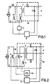
- the DC-DC converter is designed as a single-ended flow converter G1.
- the current source Q is connected on the one hand via a choke DR to the collector of a transistor T2 and on the other hand to the emitter of the transistor T2.
- a series circuit is active, which consists of the primary winding of a transformer U and the collector-emitter path of a transistor T1.
- the connections of the secondary winding of the transformer U are connected to one another via a series connection of a diode D1 and a capacitor C.
- Parallel to this capacitance C are the output A of the power supply circuit and the input of the regulator R, the output of which is connected both to the base of the transistor T2 and via an inverter 1 to the base of the transistor T1.
- the transformer U, the diode D1, the capacitance C and the transistor T1 form an unregulated Eintakt befiußwandier without storage choke in the output circuit. Its mode of action should not be discussed in more detail here, since it is already explained in detail in the cited literature reference.
- the controller R controls the transistor T2 directly and the transistor T1 via the inverter I, so that both transistors are operated in phase opposition.
- the transistor T1 is conductive - the transistor T2 then blocks - the current source delivers 0 energy to the DC converter G1.
- the transistor T2 is conductive during the blocking phase of the transistor T1, the current source Q does not run empty, but is short-circuited if the line resistance is neglected. Both transistors may never block at the same time, but they may conduct at the same time.
- a high voltage cannot build up at the input of the power supply circuit, as would be the case when idling, so that the power loss of the power supply circuit and thus the load on the power source remain low.
- a voltage source is not loaded at all when it is idling, but the most heavily when it is short-circuited. The case is exactly the opposite for a power source.
- a current source is most heavily loaded with a high-impedance load, while it is not loaded at all in the event of a short circuit.
- the choke DR serves to prevent current peaks in the transistors T1 and T2 and voltage jumps on the line, which can occur during the switching of the two transistors as a result of parasitic line capacitances. Without the choke DR, the line to the current source Q would therefore not be suppressed; in this case, the current source 0 would be connected to a power supply circuit that is not without feedback.
- FIG. 2 shows a second exemplary embodiment of the invention, the DC-DC converter of which is a push-pull flow converter G2.
- Parallel to the poles of the direct current source Q is a series circuit comprising a choke DR and the collector-emitter path of a transistor T2, the emitter of which is connected to the emitters of two further transistors T1 and T3.
- the collectors of the two transistors T1 and T3 are connected to one another via the primary winding of the transformer U, the center tap of which is connected to the collector of the transistor T2.
- the connections of the secondary winding are connected to one another via two oppositely polarized diodes D1 and D2. Between the connection point of the two diodes D1 and D2 and the center tap of the secondary winding there is a capacitance C, parallel to it are the output A of the power supply circuit and the input of the regulator R.
- the base of the transistor T2 is connected to the output of the regulator R.
- the bases of the remaining transistors T1 and T3 are connected to a clock generator TG, which in turn drives them with a square-wave voltage, the duty cycle of which is 1/2.
- the controller R and the clock generator TG are frequency-synchronized.
- the push-pull converter is made up of the transformer U, the transistors T1 and T3, the diodes D1 and D2 and the capacitance C. Its functioning is described in the literature mentioned at the beginning.
- the transistor T2 is pulse width controlled by the regulator R. As long as it blocks, coming from the current source Q, the remote feed current flows either via the transistor T1 or T3 into the primary circuit of the transformer U, because the two transistors' T1 and T3 are driven in push-pull, so that one of them is always conductive. The longer the transistor T2 is conductive, the lower the voltage at the input E of the power supply circuit and thus the load on the current source.
Landscapes
- Engineering & Computer Science (AREA)
- Power Engineering (AREA)
- Dc-Dc Converters (AREA)
Description
- Die Erfindung betrifft eine Stromversorgungsschaltung gemäß Oberbegriff des Anspruches 1. In der Zeitschrift Elektronik, 1978, Heft 4, Seite 102 bis 107 sind verschiedene Stromversorgungsschaltungen beschrieben, die mit einem Gleichspannungswandler aufgebaut sind. Es gibt zwei Grundtypen von Gleichspannungswandlern : den Sperrwandler und den Durchflußwandler. Der Gegentaktwandler ist ein Sonderfall des DurchfluBwandlers.
- Bei allen Gleichspannungswandlern wird die Eingangsspannung mittels eines Schalttransistors zerhackt. Die so erhaltene Rechteckspannung wird mit Hilfe eines Transformators übersetzt und anschließend gleichgerichtet und gesiebt Die gesiebte Ausgangsspannung des Gleichspannungswandlers wird dadurch stabilisiert, daß mit Hilfe einer Regelschaltung das Tastverhältnis der Rechteckspannung geregelt wird. Schwankungen der zu transformierenden Spannung oder des Lastwiderstandes, der mit der gesiebten Ausgangsspannung gespeist wird, bewirken deshalb eine Veränderung des Tastverhältnisses. Man spricht bei einer Regelung des Tastverhältnisses auch von Impulsbreitensteuerung.
- In der Übertragungstechnik werden Stromversorgungsschaltungen, die über eine Leitung von einer Gleichspannungsquelle ferngespeist werden, in Endgeräten und Zwischenverstärkern verwendet. Eine derartige Fernspeisung mittels einer Gleichspannungsquelle als Femspeisequelle ist bis zu einer Leitungslänge von etwa 2 km sinnvoll, weil die Spannungsverluste längs der Leitung dabei noch in einem erträglichen Maß bleiben. Wenn dagegen über eine größere Entfernung, bis z. B. 130 km, wie es in der TF-Technik oft der Fall ist, femgespeist werden soll, so ersetzt man die Gleichspannungsquelle durch eine Gleichstromquelle, die einen konstanten Strom durch die Femspeiseleitung zu dem oder den einzelnen Verbrauchern, z. B. Zwischenverstärkem, schickt. Wenn mehrere Verbraucher von derselben Femspeisequelle versorgt werden, so sind alle Verbraucher bei Verwendung einer Gleichstromquelle in Reihe zur Stromquelle geschaltet, während sie bei Verwendung einer Gleichspannungsquelle parallel zur Spannungsquelle geschaltet sind. Damit die Spannungsverluste längs der Leitung gering bleiben, muß der Strom klein sein. Deshalb ist bei einer Spannungsquelle als Energiequelle eine hohe Spannung, bei einer Stromquelle als Energiequelle ein geringer Strom von Vorteil. Sofern bei Speisung mit einer Stromquelle unterschiedliche Ströme oder Ströme, die größer als der Fernspeisestrom sind, benötigt werden, ist für jeden Verbraucher eine Stromversorgungsschaltung vorzusehen, die den Femspeisestrom in den Betriebsstrom für den Verbraucher umwandelt.
- Die in der angeführten Literaturstelle angegebenen Stromversorgungsschaltungen sind jedoch weniger dafür geeignet, einen von einer Gleichstromquelle gelieferten Strom in einen höheren Strom umzuwandeln, weil in diesem Anwendungsfall bei Verringerung der Last am Ausgang der Eingangswiderstand und damit auch die Eingangsleistung erhöht anstatt verringert werden. Sie weisen deshalb eine relativ hohe Verlustleistung auf.
- Aus der JP-A-57 62 780 ist ein Wandler bekannt, bei dem ein geglätteter Strom durch einen zweiten Transistor erzielt wird, der parallel zum Gleichspannungseingang des Wandlers mit Parallelschwing Kreis liegt und im Gegentakt zum Wandler transistor schaltet ; doch weist der Wandler keine Impulsbreitenregelung auf.
- Es ist daher Aufgabe der Erfindung, eine Stromversorgungsschaltung anzugeben, die bei Speisung durch eine Gleichstromquelle eine relativ geringe Verlustleistung aufweist.
- Die Erfindung löst diese Aufgabe mit den im Kennzeichen des Anspruches 1 stehenden Merkmalen.
- In den abhängigen Ansprüchen sind vorteilhafte Ausführungen der Erfindung angegeben.
- An Hand der in den Fig. 1 und 2 gezeigten Ausführungsbeispiele wird die Erfindung näher erläutert.
- Bei dem in der Fig. 1 dargestellten Ausführungsbeispiel ist der Gleichspannungswandler als Eintaktdurchflußwandler G1 ausgebildet. Die Stromquelle Q ist einerseits über eine Drossel DR mit dem Kollektor eines Transistors T2 und andererseits mit dem Emitter des Transistors T2 verbunden. Parallel zur Kollektor-Emitter-Strecke des Transistors T2 leigt eine Reihenschaltung, die aus der Primärwicklung eines Übertragers Ü und der Kollektor-Ernitter-Strecke eines Transistors T1 besteht. Die Anschlüsse der Sekundärwicklung des Übertragers Ü sind über eine Reihenschaltung aus einer Diode D1 und einer Kapazität C miteinander verbunden. Parallel zu dieser Kapazität C liegen der Ausgang A der Stromversorgungsschaltung sowie der Eingang des Reglers R, dessen Ausgang sowohl mit der Basis des Transistors T2 als auch über einen Inverter 1 mit der Basis des Transistors T1 verbunden ist.
- Der Übertrager Ü, die Diode D1, die Kapazität C sowie der Transistor T1 bilden einen ungeregelten Eintaktdurchfiußwandier ohne Speicherdrossel im Ausgangskreis. Auf seine Wirkungsweise soll an dieser Stelle nicht näher eingegangen werden, denn sie ist bereits in der genannten Literaturstelle ausführlich erläutert.
- Mit dem Regler R wird das Tastverhältnis der Rechteckspannung für die Transistoren T1 und T2 verändert. Der Regler R steuert den Transistor T2 unmittelbar und den Transistor T1 über den Inverter I an, so daB beide Transistoren gegenphasig betrieben werden. Während der Transistor T1 leitend ist - der Transistor T2 sperrt dann -, gibt die Stromquelle 0 Energie an den Gleichspannungswandler G1 ab. Weil der Transistor T2 während der Sperrphase des Transistors T1 leitend ist, läuft die Stromquelle Q nicht leer, sondern ist, sofern der Leitungswiderstand vernachläßigt wird, kurzgeschlossen. Es dürfen zwar nie beide Transistoren gleichzeitig sperren, wohl aber dürfen sie gleichzeitig leiten. Deshalb kann sich am Eingang der Stromversorgungsschaltung keine hohe Spannung aufbauen, wie es bei Leerlauf der Fall wäre, so daß die Verlustleistung der Stromversorgungsschaltung und damit auch die Belastung der Stromquelle gering bleiben. Zum besseren Verständnis der Funktionsweise der Erfindung sei an dieser Stelle an die unterschiedliche Belastung einer Spannungsquelle und einer Stromquelle sowohl bei Kurzschluß als auch bei Leerlauf erinnert : eine Spannungsquelle wird bei Leerlauf überhaupt nicht, dagegen bei Kurzschluß am stärksten belastet. Bei einer Stromquelle liegt der Fall genau umgekehrt. Eine Stromquelle wird bei hochohmiger Last am stärksten belastet, während sie bei Kurzschluß gar nicht belastet wird.
- Die Drossel DR dient dazu, Stromspitzen in den Transistoren T1 und T2 und Spannungssprünge auf der Leitung, die während des Schaltens der beiden Transistoren in Folge parasitärer Leitungskapazitäten auftreten können, zu verhindern. Ohne die Drossel DR wäre die Leitung zur Stromquelle Q deshalb nicht entstört, die Stromquelle 0 würde in diesem Fall mit einer nicht rückwirkungsfreien Stromversorgungsschaltung verbunden sein.
- In der Fig. 2 ist ein zweites Ausführungsbeispiel der Erfindung gezeigt, dessen Gleichspannungswandler ein Gegentaktdurchflußwandler G2 ist.
- Parallel zu den Polen der Gleichstromquelle Q liegt eine Reihenschaltung aus einer Drossel DR und der Kollektor-Emitter-Strecke eines Transistors T2, dessen Emitter mit den Emittern zweier weiterer Transistoren T1 und T3 verbunden ist. Die Kollektoren der beiden Transistoren T1 und T3 sind über die Primärwicklung des Übertragers Ü miteinander verbunden, deren Mittenanzapfung an den Kollektor des Transistors T2 angeschlossen ist. Die Anschlüsse der Sekundärwicklung sind über zwei entgegengesetzt gepolte Dioden D1 und D2 miteinander verbunden. Zwischen dem Verbindungspunkt der beiden Dioden D1 und D2 sowie der Mittenanzapfung der Sekundärwicklung liegt eine Kapazität C, parallel zu ihr liegen der Ausgang A der Stromversorgungsschaltung sowie der Eingang des Reglers R. Die Basis des Transistors T2 ist an den Ausgang des Reglers R angeschlossen. Die Basen der restlichen Transistoren T1 und T3 sind mit einem Taktgenerator TG verbunden, der sie im Gegentakt mit einer Rechteckspannung ansteuert, deren Tastverhältnis 1/2 beträgt. Der Regler R und der Taktgenerator TG sind frequenzsynchronisiert. Der Gegentaktwandler ist aus dem Übertrager Ü, den Transistoren T1 und T3, den Dioden D1 und D2 und der Kapazität C aufgebaut. Seine Funktionsweise ist in der eingangs genannten Literaturstelle beschrieben.
- Der Transistor T2 wird vom Regler R impulsbreitengesteuert. Solange er sperrt, fließt von der Stromquelle Q kommend der Fernspeisestrom entweder über den Transistor T1 oder T3 in den Primärkreis des Übertragers Ü, denn die beiden Transistoren 'T1 und T3 werden im Gegentakt angesteuert, so daß immer einer von ihnen leitend ist. Je länger der Transistor T2 leitend ist, desto geringer ist die Spannung am Eingang E der Stromversorgungsschaltung und damit die Belastung der Stromquelle.
Claims (7)
Applications Claiming Priority (2)
| Application Number | Priority Date | Filing Date | Title |
|---|---|---|---|
| DE3221404 | 1982-06-05 | ||
| DE19823221404 DE3221404A1 (de) | 1982-06-05 | 1982-06-05 | Stromversorgungsschaltung |
Publications (2)
| Publication Number | Publication Date |
|---|---|
| EP0099596A1 EP0099596A1 (de) | 1984-02-01 |
| EP0099596B1 true EP0099596B1 (de) | 1986-09-10 |
Family
ID=6165507
Family Applications (1)
| Application Number | Title | Priority Date | Filing Date |
|---|---|---|---|
| EP83200810A Expired EP0099596B1 (de) | 1982-06-05 | 1983-06-03 | Stromversorgungsschaltung |
Country Status (4)
| Country | Link |
|---|---|
| EP (1) | EP0099596B1 (de) |
| JP (1) | JPS58218871A (de) |
| CA (1) | CA1206521A (de) |
| DE (2) | DE3221404A1 (de) |
Families Citing this family (12)
| Publication number | Priority date | Publication date | Assignee | Title |
|---|---|---|---|---|
| US4595873A (en) * | 1984-07-13 | 1986-06-17 | Siemens Aktiengesellschaft | Circuit arrangement for feeding electrical users with a DC voltage |
| US4626766A (en) * | 1984-07-13 | 1986-12-02 | Siemens Aktiengesellschaft | Circuit arrangement for feeding electrical users |
| US4620271A (en) * | 1984-07-13 | 1986-10-28 | Siemens Aktiengesellschaft | Circuit arrangement for feeding electrical users via a switch controller |
| DE3427520A1 (de) * | 1984-07-26 | 1986-02-06 | Thyssen Industrie Ag, 4300 Essen | Schaltungsanordnung zur speisung eines verbraucherzweipols |
| JPH0744827B2 (ja) * | 1986-11-06 | 1995-05-15 | 株式会社東芝 | 電源装置 |
| US4924369A (en) * | 1988-01-26 | 1990-05-08 | Siemens Aktiengesellschaft | Regulated blocking converter wherein switch conduction time increases with higher output voltages |
| ES2060836T3 (es) * | 1990-03-09 | 1994-12-01 | Siemens Nixdorf Inf Syst | Fuente de alimentacion de conexion que evita picos de corriente de entrada con admision de corriente senoidal. |
| ES2086803T3 (es) * | 1993-02-26 | 1996-07-01 | Siemens Nixdorf Inf Syst | Disposicion de circuito para la activacion de los elementos de conexion de un convertidor de tension ascendente-descendente. |
| DE19531758A1 (de) * | 1995-03-22 | 1996-10-02 | Siemens Ag Albis | AC/DC-Wandler mit sinusförmiger Stromaufnahme |
| WO1998040961A2 (en) * | 1997-03-12 | 1998-09-17 | Koninklijke Philips Electronics N.V. | A convertor, a power supply, and a battery charger |
| US6124778A (en) * | 1997-10-14 | 2000-09-26 | Sun Microsystems, Inc. | Magnetic component assembly |
| JP6507602B2 (ja) * | 2014-12-03 | 2019-05-08 | 株式会社リコー | 電源装置 |
Family Cites Families (2)
| Publication number | Priority date | Publication date | Assignee | Title |
|---|---|---|---|---|
| DD99705A1 (de) * | 1972-11-20 | 1973-08-20 | ||
| US4124884A (en) * | 1977-03-07 | 1978-11-07 | Bell Telephone Laboratories, Incorporated | DC to DC converter with regulated input impedance |
-
1982
- 1982-06-05 DE DE19823221404 patent/DE3221404A1/de not_active Withdrawn
-
1983
- 1983-06-02 CA CA000429483A patent/CA1206521A/en not_active Expired
- 1983-06-03 EP EP83200810A patent/EP0099596B1/de not_active Expired
- 1983-06-03 DE DE8383200810T patent/DE3366032D1/de not_active Expired
- 1983-06-03 JP JP58098111A patent/JPS58218871A/ja active Pending
Non-Patent Citations (1)
| Title |
|---|
| Patent Abstracts of Japan, Band 6, N4. 140, 29. Juli 1982 * |
Also Published As
| Publication number | Publication date |
|---|---|
| JPS58218871A (ja) | 1983-12-20 |
| CA1206521A (en) | 1986-06-24 |
| DE3221404A1 (de) | 1983-12-08 |
| EP0099596A1 (de) | 1984-02-01 |
| DE3366032D1 (en) | 1986-10-16 |
Similar Documents
| Publication | Publication Date | Title |
|---|---|---|
| DE69226300T2 (de) | Gleichspannungswandler | |
| DE68916995T2 (de) | Schaltleistungsversorgung. | |
| DE69719945T2 (de) | Pulsbreitenmodulierter nullspannungsschaltender Halbbrücken-Gleichspannungssperrwandler | |
| DE60120800T2 (de) | Schaltnetzteileinheit | |
| DE69119848T2 (de) | Festfrequenter Einrichtungsdurchlassumformer mit Nullspannungsschaltung | |
| DE69302461T2 (de) | Spannungssteuerschaltungen | |
| DE60109504T2 (de) | Resonanter Leistungsumwandler | |
| DE69014688T2 (de) | Selbstschwingender Wandler mit Leichtlast-Stabilisator. | |
| DE3616437A1 (de) | Integrierte magnetische anordnung fuer eine elektronische schaltspannungsquelle | |
| DE69116945T2 (de) | Sperrschwinger-Schaltnetzteil für eine Anzeigevorrichtung | |
| DE2917926A1 (de) | Gegentakt-schaltleistungsverstaerker | |
| DE2935811A1 (de) | Geschalteter spannungswandler | |
| DE69818298T2 (de) | Frequenzwandler und unterbrechungsfreie stromversorgung damit | |
| EP0099596B1 (de) | Stromversorgungsschaltung | |
| DE60101234T2 (de) | Schaltnetzteilgerät | |
| DE69831267T2 (de) | Ladeschaltung für usv | |
| DE10238606B4 (de) | Schaltnetzteil | |
| DE2647146C2 (de) | Spannungsregler | |
| EP4289051A1 (de) | Primärseitig seriell verschaltete sperrwandler mit klemmschaltung | |
| EP1867035A1 (de) | Verfahren zum betreiben eines schaltnetzteils mit rückspeisung primärseitiger streuenergie | |
| DE2611439C2 (de) | Leistungsversorgungsschaltkreis mit hohem Wirkungsgrad | |
| EP0475296B1 (de) | Getaktete Stromversorgunseinrichtung mit einem Fluss- und einem Sperrwandlerausgang | |
| EP1237268A2 (de) | Spannungskonverter | |
| DE112009001775T5 (de) | Isolierte Leistungsversorgungsschalteinrichtung | |
| EP0302433B1 (de) | Sperrumrichter |
Legal Events
| Date | Code | Title | Description |
|---|---|---|---|
| PUAI | Public reference made under article 153(3) epc to a published international application that has entered the european phase |
Free format text: ORIGINAL CODE: 0009012 |
|
| AK | Designated contracting states |
Designated state(s): DE FR GB IT SE |
|
| 17P | Request for examination filed |
Effective date: 19840913 |
|
| GRAA | (expected) grant |
Free format text: ORIGINAL CODE: 0009210 |
|
| AK | Designated contracting states |
Kind code of ref document: B1 Designated state(s): DE FR GB IT SE |
|
| REF | Corresponds to: |
Ref document number: 3366032 Country of ref document: DE Date of ref document: 19861016 |
|
| ITF | It: translation for a ep patent filed | ||
| ET | Fr: translation filed | ||
| PLBE | No opposition filed within time limit |
Free format text: ORIGINAL CODE: 0009261 |
|
| STAA | Information on the status of an ep patent application or granted ep patent |
Free format text: STATUS: NO OPPOSITION FILED WITHIN TIME LIMIT |
|
| 26N | No opposition filed | ||
| PGFP | Annual fee paid to national office [announced via postgrant information from national office to epo] |
Ref country code: GB Payment date: 19910603 Year of fee payment: 9 |
|
| PGFP | Annual fee paid to national office [announced via postgrant information from national office to epo] |
Ref country code: FR Payment date: 19910621 Year of fee payment: 9 |
|
| PGFP | Annual fee paid to national office [announced via postgrant information from national office to epo] |
Ref country code: SE Payment date: 19910627 Year of fee payment: 9 |
|
| ITTA | It: last paid annual fee | ||
| PGFP | Annual fee paid to national office [announced via postgrant information from national office to epo] |
Ref country code: DE Payment date: 19910823 Year of fee payment: 9 |
|
| PG25 | Lapsed in a contracting state [announced via postgrant information from national office to epo] |
Ref country code: GB Effective date: 19920603 |
|
| PG25 | Lapsed in a contracting state [announced via postgrant information from national office to epo] |
Ref country code: SE Effective date: 19920604 |
|
| GBPC | Gb: european patent ceased through non-payment of renewal fee |
Effective date: 19920603 |
|
| PG25 | Lapsed in a contracting state [announced via postgrant information from national office to epo] |
Ref country code: FR Effective date: 19930226 |
|
| PG25 | Lapsed in a contracting state [announced via postgrant information from national office to epo] |
Ref country code: DE Effective date: 19930302 |
|
| REG | Reference to a national code |
Ref country code: FR Ref legal event code: ST |
|
| EUG | Se: european patent has lapsed |
Ref document number: 83200810.6 Effective date: 19930109 |