EP0098935A1 - Negative ion beam etching process - Google Patents
Negative ion beam etching process Download PDFInfo
- Publication number
- EP0098935A1 EP0098935A1 EP83104579A EP83104579A EP0098935A1 EP 0098935 A1 EP0098935 A1 EP 0098935A1 EP 83104579 A EP83104579 A EP 83104579A EP 83104579 A EP83104579 A EP 83104579A EP 0098935 A1 EP0098935 A1 EP 0098935A1
- Authority
- EP
- European Patent Office
- Prior art keywords
- hydrogen
- substrate
- layer
- target
- negative
- Prior art date
- Legal status (The legal status is an assumption and is not a legal conclusion. Google has not performed a legal analysis and makes no representation as to the accuracy of the status listed.)
- Granted
Links
- 238000000034 method Methods 0.000 title claims abstract description 33
- 238000005530 etching Methods 0.000 title claims abstract description 20
- 238000010884 ion-beam technique Methods 0.000 title claims abstract description 7
- 239000001257 hydrogen Substances 0.000 claims abstract description 44
- 229910052739 hydrogen Inorganic materials 0.000 claims abstract description 44
- VYPSYNLAJGMNEJ-UHFFFAOYSA-N silicon dioxide Inorganic materials O=[Si]=O VYPSYNLAJGMNEJ-UHFFFAOYSA-N 0.000 claims abstract description 44
- 150000002500 ions Chemical class 0.000 claims abstract description 39
- 239000000758 substrate Substances 0.000 claims abstract description 39
- UFHFLCQGNIYNRP-UHFFFAOYSA-N Hydrogen Chemical compound [H][H] UFHFLCQGNIYNRP-UHFFFAOYSA-N 0.000 claims abstract description 35
- XKRFYHLGVUSROY-UHFFFAOYSA-N Argon Chemical compound [Ar] XKRFYHLGVUSROY-UHFFFAOYSA-N 0.000 claims abstract description 20
- 239000000377 silicon dioxide Substances 0.000 claims abstract description 18
- 229910052786 argon Inorganic materials 0.000 claims abstract description 11
- 229910052681 coesite Inorganic materials 0.000 claims abstract description 10
- 229910052906 cristobalite Inorganic materials 0.000 claims abstract description 10
- 229910052682 stishovite Inorganic materials 0.000 claims abstract description 10
- 229910052905 tridymite Inorganic materials 0.000 claims abstract description 10
- -1 hydrogen compound Chemical class 0.000 claims abstract description 5
- 150000008040 ionic compounds Chemical class 0.000 claims abstract description 3
- 239000000463 material Substances 0.000 claims description 14
- 229910052581 Si3N4 Inorganic materials 0.000 claims description 11
- 239000004065 semiconductor Substances 0.000 claims description 8
- 239000002184 metal Substances 0.000 claims description 3
- 229910052751 metal Inorganic materials 0.000 claims description 3
- 238000002294 plasma sputter deposition Methods 0.000 claims description 2
- 239000011810 insulating material Substances 0.000 claims 2
- 239000007789 gas Substances 0.000 abstract description 25
- 229910052710 silicon Inorganic materials 0.000 abstract description 3
- 238000004544 sputter deposition Methods 0.000 description 32
- 239000002245 particle Substances 0.000 description 10
- HQVNEWCFYHHQES-UHFFFAOYSA-N silicon nitride Chemical compound N12[Si]34N5[Si]62N3[Si]51N64 HQVNEWCFYHHQES-UHFFFAOYSA-N 0.000 description 10
- 230000000694 effects Effects 0.000 description 9
- 238000000992 sputter etching Methods 0.000 description 8
- 150000002431 hydrogen Chemical class 0.000 description 5
- 230000007935 neutral effect Effects 0.000 description 5
- 125000004429 atom Chemical group 0.000 description 4
- 230000003247 decreasing effect Effects 0.000 description 4
- XUIMIQQOPSSXEZ-UHFFFAOYSA-N Silicon Chemical compound [Si] XUIMIQQOPSSXEZ-UHFFFAOYSA-N 0.000 description 2
- QVGXLLKOCUKJST-UHFFFAOYSA-N atomic oxygen Chemical compound [O] QVGXLLKOCUKJST-UHFFFAOYSA-N 0.000 description 2
- 150000001875 compounds Chemical class 0.000 description 2
- 230000002708 enhancing effect Effects 0.000 description 2
- 239000012212 insulator Substances 0.000 description 2
- 238000004519 manufacturing process Methods 0.000 description 2
- 150000002739 metals Chemical class 0.000 description 2
- 239000001301 oxygen Substances 0.000 description 2
- 229910052760 oxygen Inorganic materials 0.000 description 2
- 239000010703 silicon Substances 0.000 description 2
- KRHYYFGTRYWZRS-UHFFFAOYSA-M Fluoride anion Chemical compound [F-] KRHYYFGTRYWZRS-UHFFFAOYSA-M 0.000 description 1
- 229910004299 TbF3 Inorganic materials 0.000 description 1
- 230000002411 adverse Effects 0.000 description 1
- 230000015572 biosynthetic process Effects 0.000 description 1
- 230000007423 decrease Effects 0.000 description 1
- 230000005684 electric field Effects 0.000 description 1
- 230000017525 heat dissipation Effects 0.000 description 1
- 239000011261 inert gas Substances 0.000 description 1
- 229910001635 magnesium fluoride Inorganic materials 0.000 description 1
- 238000004377 microelectronic Methods 0.000 description 1
- 229910052594 sapphire Inorganic materials 0.000 description 1
- 239000010980 sapphire Substances 0.000 description 1
- 235000012239 silicon dioxide Nutrition 0.000 description 1
- LKNRQYTYDPPUOX-UHFFFAOYSA-K trifluoroterbium Chemical compound F[Tb](F)F LKNRQYTYDPPUOX-UHFFFAOYSA-K 0.000 description 1
- XLYOFNOQVPJJNP-UHFFFAOYSA-N water Chemical compound O XLYOFNOQVPJJNP-UHFFFAOYSA-N 0.000 description 1
Images


Classifications
-
- H—ELECTRICITY
- H01—ELECTRIC ELEMENTS
- H01L—SEMICONDUCTOR DEVICES NOT COVERED BY CLASS H10
- H01L21/00—Processes or apparatus adapted for the manufacture or treatment of semiconductor or solid state devices or of parts thereof
- H01L21/02—Manufacture or treatment of semiconductor devices or of parts thereof
- H01L21/04—Manufacture or treatment of semiconductor devices or of parts thereof the devices having potential barriers, e.g. a PN junction, depletion layer or carrier concentration layer
- H01L21/18—Manufacture or treatment of semiconductor devices or of parts thereof the devices having potential barriers, e.g. a PN junction, depletion layer or carrier concentration layer the devices having semiconductor bodies comprising elements of Group IV of the Periodic Table or AIIIBV compounds with or without impurities, e.g. doping materials
- H01L21/30—Treatment of semiconductor bodies using processes or apparatus not provided for in groups H01L21/20 - H01L21/26
- H01L21/302—Treatment of semiconductor bodies using processes or apparatus not provided for in groups H01L21/20 - H01L21/26 to change their surface-physical characteristics or shape, e.g. etching, polishing, cutting
- H01L21/306—Chemical or electrical treatment, e.g. electrolytic etching
- H01L21/3065—Plasma etching; Reactive-ion etching
Definitions
- etching methods use ion beams, neutral atoms, reactive gases, etc. for the removal of layers of different materials, including metals, insulators, and semiconductors.
- Negative ions have been found in low discharge sputtering systems and have been used to produce etched substrates by physical sputtering processes, as described in US-A-4,132,614 and 4,250,009.
- a highly ionic target is struck by an energetic particle, such as argon atoms, neutrons, ions, or other particles to produce negative ions which are then accelerated to a sample to be etched.
- the ionic targets are typically compounds which will release negative ion species such as F, Cl, Br, and I.
- the negative ions from the target will be accelerated by the fall potential (the potential between the negative target and the plasma) ta impinge upon the sample (substrate) in order to etch it.
- the negative ion may lose electrons in the plasma, it will be sufficiently accelerated to strike the substrate as an energetic neutral particle.
- negative ion etching has advantages in the etching of various materials, it would be desirable to be able to control that process in order to provide selective etching. For example, in the fabrication of semiconductor devices, it is often advantageous to have SiO 2 etch at a much more rapid rate than Si. Further, Si 3 N 4 may also be found on the semiconductor devices and advantages result when Si 3 N 4 has a different etch rate from those of Si and Si02. Heretofore, no good way has been taught or suggested for controlling the relative etch rate of different materials in a negative ion etching system.
- a negative ion beam etching process comprising plasma sputtering negative ions from a target and accelerating the negative ions to a substrate to cause etching thereof, is characterised, according to the invention, by the plasma containing hydrogen or a hydrogen compound in order to modify the etch-rate of the substrate.
- the presense of hydrogen produces a significant effect on the etch rates of different materials in this negative ion etching system.
- FIG. 1 illustrates the process of the present invention wherein a target 10 is held at a negative potential V which is measured with respect to the walls of the sputtering chamber (substantially ground).
- a sputtering gas comprising, substantially, argon ions (Ar + ) impinges upon the target 10 to release negative ions therefrom.
- the sputtering gas includes not only the traditionally used inert gases Ar, Ne, Kr, etc., but also hydrogen.
- the hydrogen is introduced into the sputtering gas as either H 2 , or as a material which will yield hydrogen.
- water vapor and other compounds of hydrogen, preferably gaseous ones can be used for this purpose.
- the presence of hydrogen in the gas used to sputter negative ions from target 10 dramatically affects the etch rates achieved in a negative ion etching process.
- the negative ions released from the target 10, indicated by the arrows F are accelerated to the full fall potential (the potential between the negative target and the sputtering gas plasma) to a substrate 12 which is to be etched.
- the negative ions will often lose electrons in the sputtering gas plasma and strike substrate 12 as energetic neutral particles.
- Substrate 12 is located on a substrate electrode 14, which can have a small negative bias voltage V B , measured with respect to the chamber wall.
- negative ions and/or energetic neutral particles are used for etching the substrate 12.
- Positive ions can be prevented from reaching substrate 12 in accordance with the teachings of aforementioned U.S.-A-4,250,009.
- Substrate 12 can be comprised of any material that is to be etched, including metals, insulators, and semiconductors. Particular examples will be described with respect to Si, Si0 2 , Si3N4, and A1203. In the practice of this invention, it has been found that the presence of hydrogen in the sputtering gas plasma causes dramatic changes in the relative etch rates of the substrate materials, without any accompanying adverse effects.
- the voltage V is a negative voltage for the purpose of attracting positive sputtering gas atoms from the plasma to the target, to cause release of negative ions therefrom.
- a typical range of V T is from about -250V to about -5000 or more volts (with respect to ground).
- the sputtering ions produce events at the target which result in the release of these negative ions, which are then extracted by the electric field between the target and the plasma.
- the bias voltage V B is also a negative voltage with respect to ground, and typically is about -25V to -several hundred volts. It is also of a smaller magnitude than V T . Voltage V B is used to inject electrons into the plasma, thereby enhancing ionization, and thereby also enhancing sputtering of the target.
- the hydrogen in the sputtering gas is present in an amount ranging from a few percent to about 50-75 percent, by volume. If the hydrogen is present in too small an amount, the effect on etch rates is very small while, if there is an excessive amount of hydrogen, for example in excess of 80% by volume, sputtering of the target will diminish by a large amount.
- the target 10 is at an angle to the direction of the energetic particle beam 16 used to sputter negative ions from target 10.
- Beam 16 is produced by known apparatus, as described in U. S. 4,250,009.
- Substrate 10 is located on a substrate holder (electrode 18) which is connected to a power supply 20, providing the voltage V T .
- Power supply 20 is also connected to substrate 12 to provide the substrate bias V B . Then beam 16 strikes target 10, negative ions will be released and accelerated towards substrate 12, as indicated by the arrows F .
- Endergetic particle beam 16 is used to sputter negative ions from the target 10, and contains hydrogen in order to provide selective etching of the substrate.
- Beam 16 can be comprised of energetic particles such as accelerated Ar + atoms, neutrons, ions, and other particles including combinations of atoms and other subatomic particles, such as Ar + ions or the like.
- Neutral beams 16 are often preferred because they do not generate high electrical currents at the target 10.
- an ion beam containing electrons it is often necessary to use means, such as a wire mesh grid, in front of the target to prevent drawing high electrical currents. This is also described in U.S.-A-4,250,009.
- sputtering gas argon, etc.
- sputtering gas argon, etc.
- hydrogen or a species containing hydrogen is also introduced with the sputtering gas.
- the pressures, voltages, apparatus etc., described herein and in those patents can be used in the practice of the present invention.
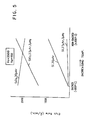
- FIGS. 3, 4, and 5 are various plots of the etch rates of Si and SiO 2 vs. bias voltage (FIGS. 3 and 4) and substrate temperature (FIG. 5). These curves illustrate the effect of the introduction of hydrogen into the sputtering gas and illustrate the striking differentials in etch rates that occur. The data upon which these curves are based is contained in the following table:
- the target was MgF 2 . Backed substrates contained a backing of GaIn to provide heat dissipation. This target had a three inch diameter and was shielded to provide a two inch opening for the sputtering plasma. A Mo substrate holder had holes therein filled with SiO 2 /Si substrate.
- the target voltage V T was -2500 V and Argon at a pressure of 4 pascals (30 microns Hg) was used as the sputtering gas.
- the substrates were not backed. No hydrogen was introduced into the sputtering gas. From these curves, it is apparent that the etch rates of both Si and SiO 2 increase as the bias voltage V B becomes more negative.
- FIG. 4 illustrates the situation in which three microns of hydrogen are present in the sputtering gas stream. Again, the substrates are non-backed. As is apparent from FIG. 4, the etch rate of Si decreases much more rapidly than the etch rate of SiO 2 when this amount of hydrogen is present. Thus, the etch rate ratio SiO 2 /Si is dramatically changed. In fact, the etch rate ratio Si0 2 /Si is about 2/1 without the hydrogen. With 10% hydrogen added to argon, the ratio is almost infinite.
- the etch rate of hot films of Si is reduced 0 from 930 to 84 A/min, with the introduction of 10% hydrogen, while the etch rate of hot films of SiO is increased from 1900 to 2300 A/min.
- the relative etch rate ratio Si 3 N 4/ Si is decreased from 780 to 57A/min, for hot films.
- the addition of 10% hydrogen causes the etch rate of silicon to be reduced to approximately 0, while the etch 0 rate of SiO 2 is decreased from 2200 to 1300 A/min.
- the etch rate ratio Si 3 N 4 /Si is approximately 0.
- a semiconductor device comprising layers of silicon (Si), silicon dioxide (SiO 2 ), and silicon nitride (Si 3 N 4 ) was etched.
- the etch rate ratio SiO 2 /Si is about 2/1 in the absence of hydrogen.
- SiO 2 silicon dioxide
- Si 3 N 4 silicon nitride
- the presence of hydrogen in the sputtering gas causes visually observable effects.
- the plasma becomes more brilliant, indicating a higher negative ion yield, such as F and possibly (HF ) in the case of MgF targets.
- the number of secondary electrons emitted from the target appeared to increase, causing further enhancement of the plasma.
Landscapes
- Engineering & Computer Science (AREA)
- Physics & Mathematics (AREA)
- Plasma & Fusion (AREA)
- Condensed Matter Physics & Semiconductors (AREA)
- General Physics & Mathematics (AREA)
- Manufacturing & Machinery (AREA)
- Computer Hardware Design (AREA)
- Microelectronics & Electronic Packaging (AREA)
- Power Engineering (AREA)
- Drying Of Semiconductors (AREA)
- Physical Deposition Of Substances That Are Components Of Semiconductor Devices (AREA)
Abstract
Description
- Many different techniques are used to etch materials, such techniques having particular importance in the fabrication of microelectronic devices including semiconductor devices. These etching methods use ion beams, neutral atoms, reactive gases, etc. for the removal of layers of different materials, including metals, insulators, and semiconductors.
- Negative ions have been found in low discharge sputtering systems and have been used to produce etched substrates by physical sputtering processes, as described in US-A-4,132,614 and 4,250,009. In this type of negative ion sputtering process, a highly ionic target is struck by an energetic particle, such as argon atoms, neutrons, ions, or other particles to produce negative ions which are then accelerated to a sample to be etched. The ionic targets are typically compounds which will release negative ion species such as F, Cl, Br, and I. Since the target is at a negative potential and the plasma surrounding the target is at approximately ground potential, the negative ions from the target will be accelerated by the fall potential (the potential between the negative target and the plasma) ta impinge upon the sample (substrate) in order to etch it. Although the negative ion may lose electrons in the plasma, it will be sufficiently accelerated to strike the substrate as an energetic neutral particle.
- Aforementioned US-A-4,132,614 and 4,250,009 describe a negative ion etching process and the different types of apparatus used to practice that process. Additionally, reference is made to J. J. Hanak, et al, "Effect of Secondary Electrons and Negative Ions on Sputtering of Films", J. Vac. Sci. Tech., Vol. 13, pp 406-409 (1976), describing an etching process using fluoride negative ions that were generated during sputtering from a TbF3 target.
- Since negative ion etching has advantages in the etching of various materials, it would be desirable to be able to control that process in order to provide selective etching. For example, in the fabrication of semiconductor devices, it is often advantageous to have SiO2 etch at a much more rapid rate than Si. Further, Si3N4 may also be found on the semiconductor devices and advantages result when Si3N4 has a different etch rate from those of Si and Si02. Heretofore, no good way has been taught or suggested for controlling the relative etch rate of different materials in a negative ion etching system.
- A negative ion beam etching process comprising plasma sputtering negative ions from a target and accelerating the negative ions to a substrate to cause etching thereof, is characterised, according to the invention, by the plasma containing hydrogen or a hydrogen compound in order to modify the etch-rate of the substrate.
- The presense of hydrogen produces a significant effect on the etch rates of different materials in this negative ion etching system.
- How the invention can be carried out will now be described by way of example, with reference to the accompanying drawings, in which:-
- FIG. 1 schematically illustrates a negative ion etching process according to the invention, in which the substrate is aligned substantially parallel to the target providing the negative etching ions;
- FIG. 2 schematically illustrates another etching process according to the invention, in which the target providing the negative etching ions is disposed at an angle to the beam used to sputter negative ions from the target;
- FIG. 3 is a plot of the etch rate of Si and Si02 vs. bias voltage, for etching of these materials without the presence of hydrogen in the sputtering gas;
- FIG. 4 is a plot of the etch rate of Si and Si02 as a function of bias voltage when hydrogen is present in the sputtering gas; and
- FIG. 5 is a plot of the etch rates of Si and SiO2 vs substrate temperature, for a situation in which hydrogen is not present in the sputtering gas and for a situation in which hydrogen is present in the sputtering gas.
- In this description, reference will be made to aforementioned US-A-4,132,614 and 4,250,009. These patents describe negative ion etching processes and suitable apparatus for these processes. Reference is also made to the previously mentioned Hanak et al article and to the references cited by Hanak et al, particularly those to Honig (Refs. 3,4). These patents and those referenced articles describe techniques for producing negative ions. The present invention uses the teachings of those patents and technical journal articles for the formation of negative ions, where those negative ions are produced by sputtering from a suitable target providing the negative ions. A particular example is the use of an ionic compound target which will yield negative ions of F, Cl, Br, and I.
- FIG. 1 illustrates the process of the present invention wherein a
target 10 is held at a negative potential V which is measured with respect to the walls of the sputtering chamber (substantially ground). A sputtering gas comprising, substantially, argon ions (Ar +) impinges upon thetarget 10 to release negative ions therefrom. In the present invention, the sputtering gas includes not only the traditionally used inert gases Ar, Ne, Kr, etc., but also hydrogen. The hydrogen is introduced into the sputtering gas as either H2, or as a material which will yield hydrogen. For example, water vapor and other compounds of hydrogen, preferably gaseous ones, can be used for this purpose. As will become apparent, the presence of hydrogen in the gas used to sputter negative ions fromtarget 10 dramatically affects the etch rates achieved in a negative ion etching process. - The negative ions released from the
target 10, indicated by the arrows F , are accelerated to the full fall potential (the potential between the negative target and the sputtering gas plasma) to asubstrate 12 which is to be etched. The negative ions will often lose electrons in the sputtering gas plasma andstrike substrate 12 as energetic neutral particles.Substrate 12 is located on asubstrate electrode 14, which can have a small negative bias voltage VB, measured with respect to the chamber wall. - In this process, negative ions and/or energetic neutral particles are used for etching the
substrate 12. Positive ions can be prevented from reachingsubstrate 12 in accordance with the teachings of aforementioned U.S.-A-4,250,009. -
Substrate 12 can be comprised of any material that is to be etched, including metals, insulators, and semiconductors. Particular examples will be described with respect to Si, Si02, Si3N4, and A1203. In the practice of this invention, it has been found that the presence of hydrogen in the sputtering gas plasma causes dramatic changes in the relative etch rates of the substrate materials, without any accompanying adverse effects. - The voltage V is a negative voltage for the purpose of attracting positive sputtering gas atoms from the plasma to the target, to cause release of negative ions therefrom. A typical range of VT is from about -250V to about -5000 or more volts (with respect to ground). The sputtering ions produce events at the target which result in the release of these negative ions, which are then extracted by the electric field between the target and the plasma.
- The bias voltage VB is also a negative voltage with respect to ground, and typically is about -25V to -several hundred volts. It is also of a smaller magnitude than VT. Voltage VB is used to inject electrons into the plasma, thereby enhancing ionization, and thereby also enhancing sputtering of the target.
- The hydrogen in the sputtering gas is present in an amount ranging from a few percent to about 50-75 percent, by volume. If the hydrogen is present in too small an amount, the effect on etch rates is very small while, if there is an excessive amount of hydrogen, for example in excess of 80% by volume, sputtering of the target will diminish by a large amount.
- In FIG. 2, the
target 10 is at an angle to the direction of theenergetic particle beam 16 used to sputter negative ions fromtarget 10. Beam 16 is produced by known apparatus, as described in U. S. 4,250,009.Substrate 10 is located on a substrate holder (electrode 18) which is connected to apower supply 20, providing the voltage VT. Power supply 20 is also connected tosubstrate 12 to provide the substrate bias VB. Thenbeam 16 strikestarget 10, negative ions will be released and accelerated towardssubstrate 12, as indicated by the arrows F . - .
Energetic particle beam 16 is used to sputter negative ions from thetarget 10, and contains hydrogen in order to provide selective etching of the substrate.Beam 16 can be comprised of energetic particles such as accelerated Ar + atoms, neutrons, ions, and other particles including combinations of atoms and other subatomic particles, such as Ar+ ions or the like.Neutral beams 16 are often preferred because they do not generate high electrical currents at thetarget 10. When an ion beam containing electrons is used, it is often necessary to use means, such as a wire mesh grid, in front of the target to prevent drawing high electrical currents. This is also described in U.S.-A-4,250,009. The introduction of the sputtering gas (argon, etc.) is in accordance with the teachings of aforementioned patents U.S.-A-4,132,614 and 4,250,009. In the practice of the present invention, hydrogen or a species containing hydrogen is also introduced with the sputtering gas. The pressures, voltages, apparatus etc., described herein and in those patents can be used in the practice of the present invention. - FIGS. 3, 4, and 5 are various plots of the etch rates of Si and SiO2 vs. bias voltage (FIGS. 3 and 4) and substrate temperature (FIG. 5). These curves illustrate the effect of the introduction of hydrogen into the sputtering gas and illustrate the striking differentials in etch rates that occur. The data upon which these curves are based is contained in the following table:

- For the data of the table, the target was MgF2. Backed substrates contained a backing of GaIn to provide heat dissipation. This target had a three inch diameter and was shielded to provide a two inch opening for the sputtering plasma. A Mo substrate holder had holes therein filled with SiO2/Si substrate.
- In FIG. 3, the target voltage VT was -2500 V and Argon at a pressure of 4 pascals (30 microns Hg) was used as the sputtering gas. The substrates were not backed. No hydrogen was introduced into the sputtering gas. From these curves, it is apparent that the etch rates of both Si and SiO2 increase as the bias voltage VB becomes more negative.
- FIG. 4 illustrates the situation in which three microns of hydrogen are present in the sputtering gas stream. Again, the substrates are non-backed. As is apparent from FIG. 4, the etch rate of Si decreases much more rapidly than the etch rate of SiO2 when this amount of hydrogen is present. Thus, the etch rate ratio SiO2/Si is dramatically changed. In fact, the etch rate ratio Si02/Si is about 2/1 without the hydrogen. With 10% hydrogen added to argon, the ratio is almost infinite.
- FIG. 5 plots the etch rates of Si and Si02 as a function of substrate temperature for the situation when no hydrogen is present and when 10% hydrogen is introduced into the argon. For these curves, VT = -2500 V, while VB = -150 V. Interestingly, the etch rate of SiO2 as a function of substrate temperature changes slope when hydrogen is present with the argon gas. At higher temperatures, slight etching of Si was observed. As will be described later, Si3N4 becomes unetched in the presence of 10% hydrogen, an effect which is also observed when the substrates are at high temperatures.
-

- Studies were also made of the etching of Si3N4 and A1203 (sapphire) in this etching apparatus. These results are illustrated in TABLE II.

- It is observed that the etch rate of hot films of Si is reduced 0 from 930 to 84 A/min, with the introduction of 10% hydrogen, while the etch rate of hot films of SiO is increased from 1900 to 2300 A/min. The relative etch rate ratio Si3N4/Si is decreased from 780 to 57A/min, for hot films.
- For low temperature films, the addition of 10% hydrogen causes the etch rate of silicon to be reduced to approximately 0, while the
etch 0 rate of SiO2 is decreased from 2200 to 1300 A/min. The etch rate ratio Si3N4/Si is approximately 0. Some data was obtained for the introduction of 10% oxygen to the system. The presence of oxygen often affected the etch rates of these materials. - In a particular example, a semiconductor device comprising layers of silicon (Si), silicon dioxide (SiO2), and silicon nitride (Si3N4) was etched. The etch rate ratio SiO2/Si is about 2/1 in the absence of hydrogen. With a 10% hydrogen addition to an argon sputtering gas, the etch rate of SiO2 decreased by about 1/3, while the etch rate of Si decreased to 0 A/min. In the absence of hydrogen, Si3N4 was etched while it was not etched with a 10% hydrogen addition to the argon sputtering gas. Thus, the process produces extreme etch rate differentials between these different materials.
- In the practice of this invention, the presence of hydrogen in the sputtering gas causes visually observable effects. The plasma becomes more brilliant, indicating a higher negative ion yield, such as F and possibly (HF ) in the case of MgF targets. Also, the number of secondary electrons emitted from the target appeared to increase, causing further enhancement of the plasma. These effects participate to produce the large effects on etch rates which are observed in this negative ion etching process.
Claims (11)
Applications Claiming Priority (2)
| Application Number | Priority Date | Filing Date | Title |
|---|---|---|---|
| US393838 | 1982-06-30 | ||
| US06/393,838 US4414069A (en) | 1982-06-30 | 1982-06-30 | Negative ion beam selective etching process |
Publications (2)
| Publication Number | Publication Date |
|---|---|
| EP0098935A1 true EP0098935A1 (en) | 1984-01-25 |
| EP0098935B1 EP0098935B1 (en) | 1986-03-26 |
Family
ID=23556447
Family Applications (1)
| Application Number | Title | Priority Date | Filing Date |
|---|---|---|---|
| EP83104579A Expired EP0098935B1 (en) | 1982-06-30 | 1983-05-10 | Negative ion beam etching process |
Country Status (4)
| Country | Link |
|---|---|
| US (1) | US4414069A (en) |
| EP (1) | EP0098935B1 (en) |
| JP (1) | JPH06105700B2 (en) |
| DE (1) | DE3362664D1 (en) |
Families Citing this family (15)
| Publication number | Priority date | Publication date | Assignee | Title |
|---|---|---|---|---|
| US4778562A (en) * | 1984-08-13 | 1988-10-18 | General Motors Corporation | Reactive ion etching of tin oxide films using neutral reactant gas containing hydrogen |
| US4544444A (en) * | 1984-08-15 | 1985-10-01 | General Motors Corporation | Reactive ion etching of tin oxide films using silicon tetrachloride reactant gas |
| US4620898A (en) * | 1985-09-13 | 1986-11-04 | The United States Of America As Represented By The Administrator Of The National Aeronautics And Space Administration | Ion beam sputter etching |
| US6942764B1 (en) * | 1995-08-24 | 2005-09-13 | Taiwan Semiconductor Manufacturing Company, Ltd. | Arc-sprayed shield for pre-sputter etching chamber |
| WO2007049402A1 (en) * | 2005-10-26 | 2007-05-03 | Sharp Kabushiki Kaisha | Process for producing film using atmospheric pressure hydrogen plasma, and method and apparatus for producing purification film |
| US7416989B1 (en) | 2006-06-30 | 2008-08-26 | Novellus Systems, Inc. | Adsorption based material removal process |
| US7977249B1 (en) | 2007-03-07 | 2011-07-12 | Novellus Systems, Inc. | Methods for removing silicon nitride and other materials during fabrication of contacts |
| US8187486B1 (en) | 2007-12-13 | 2012-05-29 | Novellus Systems, Inc. | Modulating etch selectivity and etch rate of silicon nitride thin films |
| US7981763B1 (en) * | 2008-08-15 | 2011-07-19 | Novellus Systems, Inc. | Atomic layer removal for high aspect ratio gapfill |
| US8058179B1 (en) | 2008-12-23 | 2011-11-15 | Novellus Systems, Inc. | Atomic layer removal process with higher etch amount |
| US9431268B2 (en) | 2015-01-05 | 2016-08-30 | Lam Research Corporation | Isotropic atomic layer etch for silicon and germanium oxides |
| US9425041B2 (en) | 2015-01-06 | 2016-08-23 | Lam Research Corporation | Isotropic atomic layer etch for silicon oxides using no activation |
| WO2019226341A1 (en) | 2018-05-25 | 2019-11-28 | Lam Research Corporation | Thermal atomic layer etch with rapid temperature cycling |
| KR20210019121A (en) | 2018-07-09 | 2021-02-19 | 램 리써치 코포레이션 | Electron excitation atomic layer etching |
| JP7075537B2 (en) * | 2020-02-10 | 2022-05-25 | 株式会社日立ハイテク | Plasma processing method |
Citations (3)
| Publication number | Priority date | Publication date | Assignee | Title |
|---|---|---|---|---|
| FR2332616A1 (en) * | 1975-11-24 | 1977-06-17 | Selenia Ind Elettroniche | PROCESS FOR MANUFACTURING SEMICONDUCTOR DEVICES, IN PARTICULAR BY THE CREPITATION TECHNIQUE |
| US4132614A (en) * | 1977-10-26 | 1979-01-02 | International Business Machines Corporation | Etching by sputtering from an intermetallic target to form negative metallic ions which produce etching of a juxtaposed substrate |
| US4250009A (en) * | 1979-05-18 | 1981-02-10 | International Business Machines Corporation | Energetic particle beam deposition system |
Family Cites Families (2)
| Publication number | Priority date | Publication date | Assignee | Title |
|---|---|---|---|---|
| JPS5651578A (en) * | 1979-10-01 | 1981-05-09 | Toshiba Corp | Plasma etching method |
| JPS56100421A (en) * | 1980-01-17 | 1981-08-12 | Toshiba Corp | Plasma etching method |
-
1982
- 1982-06-30 US US06/393,838 patent/US4414069A/en not_active Expired - Lifetime
-
1983
- 1983-05-10 DE DE8383104579T patent/DE3362664D1/en not_active Expired
- 1983-05-10 EP EP83104579A patent/EP0098935B1/en not_active Expired
- 1983-05-13 JP JP58082856A patent/JPH06105700B2/en not_active Expired - Lifetime
Patent Citations (3)
| Publication number | Priority date | Publication date | Assignee | Title |
|---|---|---|---|---|
| FR2332616A1 (en) * | 1975-11-24 | 1977-06-17 | Selenia Ind Elettroniche | PROCESS FOR MANUFACTURING SEMICONDUCTOR DEVICES, IN PARTICULAR BY THE CREPITATION TECHNIQUE |
| US4132614A (en) * | 1977-10-26 | 1979-01-02 | International Business Machines Corporation | Etching by sputtering from an intermetallic target to form negative metallic ions which produce etching of a juxtaposed substrate |
| US4250009A (en) * | 1979-05-18 | 1981-02-10 | International Business Machines Corporation | Energetic particle beam deposition system |
Non-Patent Citations (1)
| Title |
|---|
| JOURNAL OF VACUUM SCIENCE TECHNOLOG, vol. 13 , no. 1, 1976 J. HANAK et al. "Effect of secondary electrons and negative ions on sputtering of films" * Pages 406-409 * * |
Also Published As
| Publication number | Publication date |
|---|---|
| DE3362664D1 (en) | 1986-04-30 |
| EP0098935B1 (en) | 1986-03-26 |
| JPS599925A (en) | 1984-01-19 |
| US4414069A (en) | 1983-11-08 |
| JPH06105700B2 (en) | 1994-12-21 |
Similar Documents
| Publication | Publication Date | Title |
|---|---|---|
| EP0098935B1 (en) | Negative ion beam etching process | |
| US4259145A (en) | Ion source for reactive ion etching | |
| US4521286A (en) | Hollow cathode sputter etcher | |
| US3472751A (en) | Method and apparatus for forming deposits on a substrate by cathode sputtering using a focussed ion beam | |
| US4094764A (en) | Device for cathodic sputtering at a high deposition rate | |
| Holland | Some characteristics and uses of low‐pressure plasmas in materials science | |
| KR102044913B1 (en) | Method for generating ion beam having gallium ion and apparatus therefor | |
| JPH0635323B2 (en) | Surface treatment method | |
| US4243476A (en) | Modification of etch rates by solid masking materials | |
| Matsuo et al. | Sputtering of elemental metals by Ar cluster ions | |
| Toyoda et al. | Reactive sputtering by SF6 cluster ion beams | |
| EP0203573B1 (en) | Electron beam-excited ion beam source | |
| US6682634B1 (en) | Apparatus for sputter deposition | |
| JPH05102083A (en) | Method and apparatus for dry etching | |
| JP2849771B2 (en) | Sputter type ion source | |
| EP0360994B1 (en) | Apparatus and method for producing diamond films at low temperatures | |
| JPH11238485A (en) | Ion implanting method | |
| Ray et al. | Mechanism of production and the current density effects of doubly charged ion emission from Cd+-bombarded Nb and V targets | |
| JPH05114572A (en) | Formation of plasma containing beryllium and beryllium fluoride | |
| JPS5992995A (en) | Method for forming silicide film of high-melting metal | |
| EP0095879B1 (en) | Apparatus and method for working surfaces with a low energy high intensity ion beam | |
| JPS61248428A (en) | Apparatus for neutral high-speed particle beam | |
| JPS62130287A (en) | Method and apparatus for dry etching | |
| JPS6348933Y2 (en) | ||
| Matsuo et al. | Novel analysis techniques using cluster ion beams |
Legal Events
| Date | Code | Title | Description |
|---|---|---|---|
| PUAI | Public reference made under article 153(3) epc to a published international application that has entered the european phase |
Free format text: ORIGINAL CODE: 0009012 |
|
| AK | Designated contracting states |
Designated state(s): DE FR GB |
|
| 17P | Request for examination filed |
Effective date: 19840426 |
|
| GRAA | (expected) grant |
Free format text: ORIGINAL CODE: 0009210 |
|
| AK | Designated contracting states |
Kind code of ref document: B1 Designated state(s): DE FR GB |
|
| ET | Fr: translation filed | ||
| REF | Corresponds to: |
Ref document number: 3362664 Country of ref document: DE Date of ref document: 19860430 |
|
| PLBE | No opposition filed within time limit |
Free format text: ORIGINAL CODE: 0009261 |
|
| STAA | Information on the status of an ep patent application or granted ep patent |
Free format text: STATUS: NO OPPOSITION FILED WITHIN TIME LIMIT |
|
| 26N | No opposition filed | ||
| PGFP | Annual fee paid to national office [announced via postgrant information from national office to epo] |
Ref country code: GB Payment date: 19930427 Year of fee payment: 11 |
|
| PGFP | Annual fee paid to national office [announced via postgrant information from national office to epo] |
Ref country code: DE Payment date: 19930525 Year of fee payment: 11 |
|
| PGFP | Annual fee paid to national office [announced via postgrant information from national office to epo] |
Ref country code: FR Payment date: 19940427 Year of fee payment: 12 |
|
| PG25 | Lapsed in a contracting state [announced via postgrant information from national office to epo] |
Ref country code: GB Effective date: 19940510 |
|
| GBPC | Gb: european patent ceased through non-payment of renewal fee |
Effective date: 19940510 |
|
| PG25 | Lapsed in a contracting state [announced via postgrant information from national office to epo] |
Ref country code: DE Effective date: 19950201 |
|
| PG25 | Lapsed in a contracting state [announced via postgrant information from national office to epo] |
Ref country code: FR Effective date: 19960229 |
|
| REG | Reference to a national code |
Ref country code: FR Ref legal event code: ST |
|
| REG | Reference to a national code |
Ref country code: FR Ref legal event code: ST |