EP0098705A2 - Phase lock loop circuit - Google Patents
Phase lock loop circuit Download PDFInfo
- Publication number
- EP0098705A2 EP0098705A2 EP83303503A EP83303503A EP0098705A2 EP 0098705 A2 EP0098705 A2 EP 0098705A2 EP 83303503 A EP83303503 A EP 83303503A EP 83303503 A EP83303503 A EP 83303503A EP 0098705 A2 EP0098705 A2 EP 0098705A2
- Authority
- EP
- European Patent Office
- Prior art keywords
- signal
- phase
- sweep
- circuit
- output
- Prior art date
- Legal status (The legal status is an assumption and is not a legal conclusion. Google has not performed a legal analysis and makes no representation as to the accuracy of the status listed.)
- Granted
Links
Images


Classifications
-
- H—ELECTRICITY
- H03—ELECTRONIC CIRCUITRY
- H03L—AUTOMATIC CONTROL, STARTING, SYNCHRONISATION OR STABILISATION OF GENERATORS OF ELECTRONIC OSCILLATIONS OR PULSES
- H03L7/00—Automatic control of frequency or phase; Synchronisation
- H03L7/06—Automatic control of frequency or phase; Synchronisation using a reference signal applied to a frequency- or phase-locked loop
- H03L7/08—Details of the phase-locked loop
- H03L7/10—Details of the phase-locked loop for assuring initial synchronisation or for broadening the capture range
- H03L7/12—Details of the phase-locked loop for assuring initial synchronisation or for broadening the capture range using a scanning signal
-
- H—ELECTRICITY
- H04—ELECTRIC COMMUNICATION TECHNIQUE
- H04L—TRANSMISSION OF DIGITAL INFORMATION, e.g. TELEGRAPHIC COMMUNICATION
- H04L27/00—Modulated-carrier systems
- H04L27/18—Phase-modulated carrier systems, i.e. using phase-shift keying
- H04L27/22—Demodulator circuits; Receiver circuits
-
- H—ELECTRICITY
- H04—ELECTRIC COMMUNICATION TECHNIQUE
- H04L—TRANSMISSION OF DIGITAL INFORMATION, e.g. TELEGRAPHIC COMMUNICATION
- H04L27/00—Modulated-carrier systems
- H04L27/18—Phase-modulated carrier systems, i.e. using phase-shift keying
- H04L27/22—Demodulator circuits; Receiver circuits
- H04L27/227—Demodulator circuits; Receiver circuits using coherent demodulation
- H04L27/2271—Demodulator circuits; Receiver circuits using coherent demodulation wherein the carrier recovery circuit uses only the demodulated signals
- H04L27/2272—Demodulator circuits; Receiver circuits using coherent demodulation wherein the carrier recovery circuit uses only the demodulated signals using phase locked loops
-
- Y—GENERAL TAGGING OF NEW TECHNOLOGICAL DEVELOPMENTS; GENERAL TAGGING OF CROSS-SECTIONAL TECHNOLOGIES SPANNING OVER SEVERAL SECTIONS OF THE IPC; TECHNICAL SUBJECTS COVERED BY FORMER USPC CROSS-REFERENCE ART COLLECTIONS [XRACs] AND DIGESTS
- Y10—TECHNICAL SUBJECTS COVERED BY FORMER USPC
- Y10S—TECHNICAL SUBJECTS COVERED BY FORMER USPC CROSS-REFERENCE ART COLLECTIONS [XRACs] AND DIGESTS
- Y10S331/00—Oscillators
- Y10S331/02—Phase locked loop having lock indicating or detecting means
Definitions
- This invention relates to a phase lock loop circuit, and is especially concerned with a phase lock loop circuit for locking the phase of a recovered carrier to that of a received carrier of aPSK (Phase-Shift-Keying) signal.
- aPSK Phase-Shift-Keying
- an output obtained by detecting a received PSK signal using a recovered carrier is subjected to logical processing in order to remove phase components.
- the output signal is thai applied to a voltage controlled oscillator as a phase error signal and the phase of the recovered carrier, which carrier is output from the voltage controlled oscillator, is locked to the phase of a received PSK signal.
- a high performance loop which is less affected by disturbances, can be obtained by narrowing the loop bandwidth, but an excessively narrow loop bandwidth will invite deterioration of tracking characteristics with respect to the received PSK signal.
- a phase lock loop circuit comprising a voltage controlled oscillator arranged to be controlled in dependence upon a phase error signal, a sweep s.ignal generator operable to generate a sweep signal, and means operable to superimpose the sweep signal on the phase error signal thereby to sweep the voltage controlled oscillator, having means operable to suspend such sweeping of the voltage controlled oscillator when phase lock is achieved, characterised in that the means operable to suspend such sweeping are operable, upon achievement of phase lock, to maintain the superimposition, on the phase error signal, of the level of the sweep signal immediately before such achievement.
- Embodiments of the present invention provide phase lock loops which do not generate unwantedsweep signal components and which require only simple circuit structures.
- An embodiment of the present invention can provide a phase lock loop which has excellent tracking characteristics for a received PSK signal, and also has stable operations.
- An embodiment of the present invention provides for the prevention of generation of unwanted sweep components signal./ in a phase locking method using a sweep signal.
- a sweep signal generated from the sweep generator is applied to a voltage controlled oscillator which generates a recovered carrier in dependence upon a non-synchronous state decision signal generated by decision means in accordance with the phase lock state (locked or non-locked) of the loop, and the sweep signal generated by the sweep generator is held at the level which it possessed just before a phase locked state is established in accordance with the phase lock state decision signal generated from the decision means in the phase lock state.
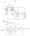
- the phase detector 2 synchronously detects the 4-level PSK signal on the basis of a recovered carrier as supplied from an output of the voltage controlled oscillator 7 and the recovered carrier as phase-shifted by 90 degrees, then demodulates data from the PSK signal and provides an output of demodulated data at the output terminals 3.
- Such data is applied to the baseband processing circuit 4 and baseband processing circuit 4 outputs a phase error signal and a decision signal b which indicates whether or not the loop is phase-locked.
- phase error signal for example in the case of the synchronous detection of a 4-level PSK signal indicated by sin ( ⁇ + n/4. ⁇ ), there is used a sin4Q signal obtained by 4-times frequency multiplication of such a signal by the baseband processing circuit 4 and by removal of phase components therefrom.
- a signal having values "1" and "0" is used as the decision signal b. These values are obtained by integrating a cos4 ⁇ signal, which is obtained as a signal having a phase difference of 90 degrees from the pertinent sin4 ⁇ signal, and then by comparing the integrated value with a specified threshold level.
- a signal value "0" is output as the decision signal b - indicating the phase locked state - and when a value smaller than the threshold level is obtained a signal value "1" is output as the"decision signal b-indicating a non-phase locked state, respectively.
- the phase error signal is applied as a control signal to the voltage controlled oscillator 7 via the loop filter 6 from the adder circuit 5, and the phase of the recovered carrier as provided from an output of the voltage controlled oscillator 7 is locked to the carrier phase of the received PSK signal applied to the input terminal.
- the decision signal b sent from the baseband processing circuit 4 is of value "1" in the non-locked condition and of value "0" in the locked condition. Therefore, the sweep signal ⁇ a sent from the sweep oscillator 8 is not applied to the voltage controlled oscillator 7 in the locked condition and the phase lock loop operates so that the phase error signal becomes zero.
- the sweep signal a is applied to the adder circuit 5 via the AND gate 10 and capacitor 9 and it is then applied via the loop filter 6 to the voltage controlled oscillator 7, as a control signal therefor, together with the phase error signal. Therefore , in the non-locked condition the output frequency of the voltage controlled oscillator 7 is swept until it is set to a pull-in condition.
- Figure 2 illustrates signal waveforms relating to the loop of Figure 1.
- the sweep signal a is indicated at waveform (a), the decision signal b at waveform (b), a signal c applied to the adder 5 via capacitor 9 at waveform (c) and the output signal d of AND gate 10 at waveform (d).
- the sweep signal a takes values "1" and "0" repeatedly- with a constant repeat period as shown in waveform (a) and is applied to the phase lock loop via the AND gate 10 when the decision signal b has value "1" indicating a non-locked state.
- the capacitor 9 is provided in order to eliminate DC coupling between the output of AND gate 10 and the phase lock loop and to output a pseudo 3-level signal. That is, a sweep in both positive and negative directions becomes possible by applying the sweep signal, consisting of a rectangular wave signal, to the loop through the capacitor 9.
- Figure 2(b)', (c)', and (d)' respectively show further examples of waveforms of the decision signal b, output signal c of capacitor 9 and output signal d of AND gate 10 and in this case since the decision signal b becomes "0" when the sweep signal a is "O", the signal applied to the phase lock loop is applied as a pseudo 3-level signal, and no problem arises.
- Figure 3 is a schematic block diagram of an embodiment of the presentinvention.
- the same reference numerals and letters as are used in Figure 1 indicate similar circuit elements and signals and 11 is a selector circuit.
- the selector circuit 11 receives the decision signal b sent from the baseband processing circuit 4 at the terminal A and outputs a signal d of similar purpose to signal d of Figure 1 but taking different values as indicated below.
- the decision signal b is "1”
- the sweep signal a which is output from the sweep oscillator 8
- the decision signal b is "O”
- output level is determined in dependence upon the level of output signal d obtained while the decisionsignal b has changed to "0' from "1”. Namely, when "0" was being output when the decision signal b changed to "0”, “0” is output after the change and when "1” was being output, "1” is output after the change, respectively.
- the decision signal b changes to "O"
- the immediately preceding condition of output d is maintained after the change and the truth value table of the selector circuit 11 is as indicated in Table 1.
- b refers to the changed value (i.e. the value after the change) of the decision signal b
- a refers to the signal a generated from the sweep generator 8
- d -1 refers to theoutput d of the selector circuit 11 just before the decision signal b changes, and refers d to the output d from the selector circuit 11, respectively.
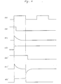
- Figure 4 illustrates signal waveforms relating to the loop of Figure 3.
- the output signal d of the selector circuit 11 is held to "1"-as shown in waveform (d)- when the decision signal b changes from "1" to "0"-as shown waveform (b).
- the output signal c of the capacitor 9 does not generate extra sweep signal components.(see Figure 2) - as evidenced by waveform (c).
- waveform (b)' of Figure 4 when the decision signal b changes from “1" to “0" while the sweep signal a is "O", the output signal d of the selector circuit 11 becomes “0” as shown in waveform (d)' and the output signal c of capacitor 9 is as indicated in waveform (c)'.
- the signal waveforms obtained are the same as waveforms (b)' to (d)' of Figure 2.
- the selector circuit 11 shown in Figure 3 can easily be formed by logic circuits based on the truth table shown in Table 1 and one structure for such a circuit 11 is shown in Figure 5.
- 110 is a flip-flop; 111, 112 are AND gates; 113 is an invertor; and 114 is an OR gate.
- the decision signal b generated by the baseband processing circuit 4 is input to a terminal C of the flip-flop 110, to invertor 113 and to AND gate 112, whilst the sweep signal a generated by the sweep oscillator 8 is input to a terminal D of flip-flop 110 and to AND gate 111.
- the output of the OR gate 114 provides the output d of the selector circuit 11.
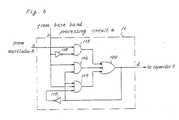
- Figure 6 illustrates another structure for such a selector circuit 11.
- 115, 116 and 117 are AND gates; 118 and 119 are invertors; and 120 is an OR gate.
- the decision signal b generated from the baseband processing circuit 4 is input to the inverter 118 and to AND gates 116 and 117, whilst the sweep signal a generated from the sweep oscillator 8 is input to the AND gate 115.
- the output of the OR gate 120 provides an output d of the selector circuit 11.
- CMOS-IC MC14052B can be adopted as said selector circuit 11.
- an embodiment of the present invention provides that sweeping is suspended in accordance with a decision signal which indicates the phase lock state and that the level of sweep signal a just before the phase lock state is achieved is held and is applied to the phase lock loop at the time of achievement of phase lock.
- Pulling in of phase involves sweeping the voltage controlled oscillator 7 by means of the sweep oscillator 8 in the phase lock loop circuit to recover carrier for demodulation of the PSK signal.
- the embodiment of this invention provides that an unwanted signal is not generated when the sweep stops and moreover that stable phase lock operation can be realized.
- the loop circuit so that the decision signal b is "O" in the non-lock state and "1" for the locked stated-different from the described embodiment.
- the logic structure of the selector circuit must be formed to correspond to the logic of the decision signal
- An embodiment of the present invention discloses a phase lock loop circuit for recovering a carrier for demodulating a PSK signal.
- a voltage controlled oscillator is swept by means of a sweep generator.
- a sweep signal is suspended in accordance with a decision signal which indicates that a phase locked state is achieved and the immediately preceding level of the sweep signal is held and applied to the phase lock loop at the timing of phase-lock pull-in. Thereby an unwanted sweep signal component is no longer generated when sweep stops and stable phase lock operation can be realized.
Landscapes
- Engineering & Computer Science (AREA)
- Computer Networks & Wireless Communication (AREA)
- Signal Processing (AREA)
- Stabilization Of Oscillater, Synchronisation, Frequency Synthesizers (AREA)
- Digital Transmission Methods That Use Modulated Carrier Waves (AREA)
Abstract
Description
- This invention relates to a phase lock loop circuit, and is especially concerned with a phase lock loop circuit for locking the phase of a recovered carrier to that of a received carrier of aPSK (Phase-Shift-Keying) signal.
- In a synchronous detection system for demodulating a received PSK signal, there must be recovered a carrier which is phase-locked to a carrier of the received PSK signal.
- Therefore, in a synchronous detecting system of this type, an output obtained by detecting a received PSK signal using a recovered carrier is subjected to logical processing in order to remove phase components. The output signal is thai applied to a voltage controlled oscillator as a phase error signal and the phase of the recovered carrier, which carrier is output from the voltage controlled oscillator, is locked to the phase of a received PSK signal.
- In an ordinary phase lock loop circuit, a high performance loop, which is less affected by disturbances, can be obtained by narrowing the loop bandwidth, but an excessively narrow loop bandwidth will invite deterioration of tracking characteristics with respect to the received PSK signal.
- Accordingly, there has been proposed a method intended to ensure stable circuit operation with excellent tracking characteristics and narrow loop bandwidth, in which method a specified sweep signal is superimposed on a phase error signal as mentioned above in order to control the voltage controlled oscillator of the phase lock loop circuit until synchronous operation of the circuit is established, and in which method supply of the sweep signal is suspended after synchronous operation is established.
- However, the method in which a superimposed sweep signal is employed has involved the generation of an extra sweep signal component at the time of suspending superimposition of such sweep signal, accordingly giving rise to a disturbance of the phase lock loop.
- According to the present invention there is provided a phase lock loop circuit, comprising a voltage controlled oscillator arranged to be controlled in dependence upon a phase error signal, a sweep s.ignal generator operable to generate a sweep signal, and means operable to superimpose the sweep signal on the phase error signal thereby to sweep the voltage controlled oscillator, having means operable to suspend such sweeping of the voltage controlled oscillator when phase lock is achieved, characterised in that the means operable to suspend such sweeping are operable, upon achievement of phase lock, to maintain the superimposition, on the phase error signal, of the level of the sweep signal immediately before such achievement.
- Embodiments of the present invention provide phase lock loops which do not generate unwantedsweep signal components and which require only simple circuit structures.
- An embodiment of the present invention can provide a phase lock loop which has excellent tracking characteristics for a received PSK signal, and also has stable operations.
- An embodiment of the present invention provides for the prevention of generation of unwanted sweep components signal./ in a phase locking method using a sweep signal.
- In a phase lock loop embodying the present invention, a sweep signal generated from the sweep generator is applied to a voltage controlled oscillator which generates a recovered carrier in dependence upon a non-synchronous state decision signal generated by decision means in accordance with the phase lock state (locked or non-locked) of the loop, and the sweep signal generated by the sweep generator is held at the level which it possessed just before a phase locked state is established in accordance with the phase lock state decision signal generated from the decision means in the phase lock state.
- Reference is made, by way of example, to the accompanying drawings, in which:-
- Figure 1 is a schematic block diagram of a previously proposed phase lock loop in which a sweep signal is superimposed on a phase error signal generated by a baseband processing circuit of the loop,
- Figure 2 is a waveform diagram illustrating output waveforms of main circuit elements of the loop illustrated in Figure 1,
- Figure 3 is a schematic block diagram of phase lock loop embodying the present invention in which sweep signal supply is controlled by a selector circuit,
- Figure 4 is a waveform diagram illustrating output waveforms of main circuit elements of the loop illustrated in Figure 3,
- Figure 5 is a logical circuit diagram of one form of selector circuit that can be employed in an embodiment of the present invention, and
- Figure 6 is a logical circuit diagram of another form of selector circuit that can be employed in an embodiment of the present invention.
- In Figure 1, 1 is an input terminal for a received PSK signal; 2 is a phase detector; 3 indicates output terminals for demodulated data; 4 is a baseband processing circuit; 5 is an adder; 6 is a loop (shownas a low-pass) filter; 7 is a voltage controlled oscillator; 8 is a sweep oscillator; 9 is a coupling capacitor; and 10 is an AND gate.
- Assuming that the received PSK signal is a 4-level PSK signal, the
phase detector 2 synchronously detects the 4-level PSK signal on the basis of a recovered carrier as supplied from an output of the voltage controlled oscillator 7 and the recovered carrier as phase-shifted by 90 degrees, then demodulates data from the PSK signal and provides an output of demodulated data at theoutput terminals 3. Such data is applied to thebaseband processing circuit 4 andbaseband processing circuit 4 outputs a phase error signal and a decision signal b which indicates whether or not the loop is phase-locked. - As the phase error signal, for example in the case of the synchronous detection of a 4-level PSK signal indicated by sin (θ + n/4.π), there is used a sin4Q signal obtained by 4-times frequency multiplication of such a signal by the
baseband processing circuit 4 and by removal of phase components therefrom. - As the decision signal b, moreover, a signal having values "1" and "0" is used. These values are obtained by integrating a cos4θ signal, which is obtained as a signal having a phase difference of 90 degrees from the pertinent sin4θ signal, and then by comparing the integrated value with a specified threshold level. The cos4θ signal becomes equal to 1 when 8 = 0 in a perfect phase locked state and becomes equal to about 0.5 where detection is carried out in respect of a non-phase-locked random signal. For example, therefore, when the specified threshold level is selected to a value of 0.75 and a value larger than such threshold level is obtained in respect of the integrated cos4θ signal,a signal value "0" is output as the decision signal b - indicating the phase locked state - and when a value smaller than the threshold level is obtained a signal value "1" is output as the"decision signal b-indicating a non-phase locked state, respectively.
- The phase error signal is applied as a control signal to the voltage controlled oscillator 7 via the
loop filter 6 from the adder circuit 5, and the phase of the recovered carrier as provided from an output of the voltage controlled oscillator 7 is locked to the carrier phase of the received PSK signal applied to the input terminal. - As mentioned above, the decision signal b sent from the
baseband processing circuit 4 is of value "1" in the non-locked condition and of value "0" in the locked condition. Therefore, the sweep signal` a sent from thesweep oscillator 8 is not applied to the voltage controlled oscillator 7 in the locked condition and the phase lock loop operates so that the phase error signal becomes zero. In the non-locked condition, the sweep signal a is applied to the adder circuit 5 via theAND gate 10 andcapacitor 9 and it is then applied via theloop filter 6 to the voltage controlled oscillator 7, as a control signal therefor, together with the phase error signal. Therefore , in the non-locked condition the output frequency of the voltage controlled oscillator 7 is swept until it is set to a pull-in condition. - Figure 2 illustrates signal waveforms relating to the loop of Figure 1. The sweep signal a is indicated at waveform (a), the decision signal b at waveform (b), a signal c applied to the adder 5 via
capacitor 9 at waveform (c) and the output signal d ofAND gate 10 at waveform (d). - The sweep signal a takes values "1" and "0" repeatedly- with a constant repeat period as shown in waveform (a) and is applied to the phase lock loop via the
AND gate 10 when the decision signal b has value "1" indicating a non-locked state. Thecapacitor 9 is provided in order to eliminate DC coupling between the output ofAND gate 10 and the phase lock loop and to output a pseudo 3-level signal. That is, a sweep in both positive and negative directions becomes possible by applying the sweep signal, consisting of a rectangular wave signal, to the loop through thecapacitor 9. - When the decision signal b changes to the locked condition value "0", from the non-locked condition value "1", the output of
AND gate 10 becomes "0" independently of the level of sweep signal a. Therefore, when the decision signal b changes to "0" while the sweep signal a is "1", an extra signal component c' occurs, as shown in Figure 2(c) through charging and discharging of thecapacitor 9. Because of this extra signal component, a pull-in state is sometimes destroyed just as when such a pull-in state is broken by a disturbance. - Figure 2(b)', (c)', and (d)' respectively show further examples of waveforms of the decision signal b, output signal c of
capacitor 9 and output signal d ofAND gate 10 and in this case since the decision signal b becomes "0" when the sweep signal a is "O", the signal applied to the phase lock loop is applied as a pseudo 3-level signal, and no problem arises. - Thus, a defect has been observed such that if phase is locked and sweep stops when the sweep signal a is "1", an extra sweep signal c' is generated, giving rise to a disturbance of the phase lock loop.
- Figure 3 is a schematic block diagram of an embodiment of the presentinvention. The same reference numerals and letters as are used in Figure 1 indicate similar circuit elements and signals and 11 is a selector circuit.
- At a terminal A the
selector circuit 11 receives the decision signal b sent from thebaseband processing circuit 4 at the terminal A and outputs a signal d of similar purpose to signal d of Figure 1 but taking different values as indicated below. When the decision signal b is "1", the sweep signal a, which is output from thesweep oscillator 8, is directly output from the selector circuit and when the decision signal b is "O", output level is determined in dependence upon the level of output signal d obtained while the decisionsignal b has changed to "0' from "1". Namely, when "0" was being output when the decision signal b changed to "0", "0" is output after the change and when "1" was being output, "1" is output after the change, respectively. In other words, when the decision signal b changes to "O", the immediately preceding condition of output d is maintained after the change and the truth value table of theselector circuit 11 is as indicated in Table 1.
- In Table 1, b refers to the changed value (i.e. the value after the change) of the decision signal b, a refers to the signal a generated from the
sweep generator 8; d-1 refers to theoutput d of theselector circuit 11 just before the decision signal b changes, and refers d to the output d from theselector circuit 11, respectively. - When the initial value of decision signal b is "0" (and the changed value "1") the value of d 1 is uncertain and the output d of
selector circuit 11 after the change is also uncertain (depends on a). - Figure 4 illustrates signal waveforms relating to the loop of Figure 3. When the sweep signal a -waveform (a)- is "1", the output signal d of the
selector circuit 11 is held to "1"-as shown in waveform (d)- when the decision signal b changes from "1" to "0"-as shown waveform (b). Thereby the output signal c of thecapacitor 9 does not generate extra sweep signal components.(see Figure 2) - as evidenced by waveform (c). - As shownby waveform (b)' of Figure 4, when the decision signal b changes from "1" to "0" while the sweep signal a is "O", the output signal d of the
selector circuit 11 becomes "0" as shown in waveform (d)' and the output signal c ofcapacitor 9 is as indicated in waveform (c)'. In this case, the signal waveforms obtained are the same as waveforms (b)' to (d)' of Figure 2. - As explained above, with the change of b from "1" to "0" the output signal d of the
selector circuit 11 holds the state "1" even when the sweep signal a is "1" (compare Figure 2, waveform (d) ) the non-lock state changes to locked state and thereby the sweep stops. Therefore, the unwanted sweep signal component which has been observedin is previously proposed loops not generated and thereby the phase lock condition can be maintained. - The
selector circuit 11 shown in Figure 3 can easily be formed by logic circuits based on the truth table shown in Table 1 and one structure for such acircuit 11 is shown in Figure 5. - In Figure 5, 110 is a flip-flop; 111, 112 are AND gates; 113 is an invertor; and 114 is an OR gate. The decision signal b generated by the
baseband processing circuit 4 is input to a terminal C of the flip-flop 110, toinvertor 113 and toAND gate 112, whilst the sweep signal a generated by thesweep oscillator 8 is input to a terminal D of flip-flop 110 and to AND gate 111. The output of theOR gate 114 provides the output d of theselector circuit 11. - Figure 6 illustrates another structure for such a
selector circuit 11. In Figure 6, 115, 116 and 117 are AND gates; 118 and 119 are invertors; and 120 is an OR gate. The decision signal b generated from thebaseband processing circuit 4 is input to theinverter 118 and to ANDgates sweep oscillator 8 is input to theAND gate 115. The output of theOR gate 120 provides an output d of theselector circuit 11. - More practically, Motorola's CMOS-IC MC14052B can be adopted as said
selector circuit 11. - As explained above, an embodiment of the present invention provides that sweeping is suspended in accordance with a decision signal which indicates the phase lock state and that the level of sweep signal a just before the phase lock state is achieved is held and is applied to the phase lock loop at the time of achievement of phase lock. Pulling in of phase involves sweeping the voltage controlled oscillator 7 by means of the
sweep oscillator 8 in the phase lock loop circuit to recover carrier for demodulation of the PSK signal. The embodiment of this invention provides that an unwanted signal is not generated when the sweep stops and moreover that stable phase lock operation can be realized. - It is of course possible to arrange the loop circuit so that the decision signal b is "O" in the non-lock state and "1" for the locked stated-different from the described embodiment. In such a case, the logic structure of the selector circuit must be formed to correspond to the logic of the decision signal
- An embodiment of the present invention discloses a phase lock loop circuit for recovering a carrier for demodulating a PSK signal. A voltage controlled oscillator is swept by means of a sweep generator. A sweep signal is suspended in accordance with a decision signal which indicates that a phase locked state is achieved and the immediately preceding level of the sweep signal is held and applied to the phase lock loop at the timing of phase-lock pull-in. Thereby an unwanted sweep signal component is no longer generated when sweep stops and stable phase lock operation can be realized.
Claims (4)
Applications Claiming Priority (2)
| Application Number | Priority Date | Filing Date | Title |
|---|---|---|---|
| JP57105205A JPS58221548A (en) | 1982-06-18 | 1982-06-18 | Phase locking circuit |
| JP105205/82 | 1982-06-18 |
Publications (3)
| Publication Number | Publication Date |
|---|---|
| EP0098705A2 true EP0098705A2 (en) | 1984-01-18 |
| EP0098705A3 EP0098705A3 (en) | 1985-07-10 |
| EP0098705B1 EP0098705B1 (en) | 1988-08-24 |
Family
ID=14401159
Family Applications (1)
| Application Number | Title | Priority Date | Filing Date |
|---|---|---|---|
| EP83303503A Expired EP0098705B1 (en) | 1982-06-18 | 1983-06-17 | Phase lock loop circuit |
Country Status (4)
| Country | Link |
|---|---|
| US (1) | US4547736A (en) |
| EP (1) | EP0098705B1 (en) |
| JP (1) | JPS58221548A (en) |
| DE (1) | DE3377853D1 (en) |
Cited By (5)
| Publication number | Priority date | Publication date | Assignee | Title |
|---|---|---|---|---|
| EP0243589A3 (en) * | 1986-02-20 | 1989-02-22 | Fujitsu Limited | Radio receiver with a carrier recovery control system |
| EP0219863A3 (en) * | 1985-10-25 | 1989-03-01 | Siemens Aktiengesellschaft Berlin Und Munchen | Lock circuit for carrier recovery from a qam signal |
| GB2215541A (en) * | 1988-02-01 | 1989-09-20 | Toshiba Kk | Carrier recovery loops |
| EP0478080A3 (en) * | 1990-09-28 | 1993-02-24 | Siemens Telecomunicazioni S.P.A. | Automatic frequency control device in coherent demodulators for m-qam modulation systems |
| RU2138907C1 (en) * | 1996-12-24 | 1999-09-27 | Самсунг Электроникс Ко., Лтд. | Device for synchronization of digital receiver |
Families Citing this family (6)
| Publication number | Priority date | Publication date | Assignee | Title |
|---|---|---|---|---|
| US4794623A (en) * | 1985-10-17 | 1988-12-27 | At&T Telephone And Telegraph Company, At&T Bell Laboratories | Recovery of carrier signal from QAM double sideband suppressed carrier IF signal for use in synchronous demodulation |
| JPS62136152A (en) * | 1985-12-09 | 1987-06-19 | Sony Corp | Synchronous detecting circuit |
| US4713630A (en) * | 1986-07-29 | 1987-12-15 | Communications Satellite Corporation | BPSK Costas-type PLL circuit having false lock prevention |
| JPH0388457A (en) * | 1989-08-30 | 1991-04-12 | Nec Eng Ltd | Sweep system for carrier recovery circuit |
| US5276716A (en) * | 1990-02-15 | 1994-01-04 | Advanced Micro Devices Inc. | Bi-phase decoder phase-lock loop in CMOS |
| JP2932861B2 (en) * | 1992-10-13 | 1999-08-09 | 日本電気株式会社 | Phase synchronization detection circuit |
Family Cites Families (7)
| Publication number | Priority date | Publication date | Assignee | Title |
|---|---|---|---|---|
| FR1468762A (en) * | 1965-08-05 | 1967-02-10 | Cit Alcatel | Synchronized frequency locking device |
| US4000476A (en) * | 1974-12-19 | 1976-12-28 | Digital Communications Corporation | Phase locked loop with circuit for preventing sidelock |
| JPS5173816A (en) * | 1974-12-24 | 1976-06-26 | Fujitsu Ten Ltd | JIDODOCHO JUSHINKI |
| JPS5821862B2 (en) * | 1976-11-11 | 1983-05-04 | 日本電気株式会社 | phase synchronized circuit |
| US4077016A (en) * | 1977-02-22 | 1978-02-28 | Ncr Corporation | Apparatus and method for inhibiting false locking of a phase-locked loop |
| US4092606A (en) * | 1977-06-21 | 1978-05-30 | Lovelace Alan M Acting Adminis | Quadraphase demodulation |
| US4131862A (en) * | 1977-10-13 | 1978-12-26 | Sperry Rand Corporation | Phase lock loop with narrow band lock-in and wideband acquisition characteristics |
-
1982
- 1982-06-18 JP JP57105205A patent/JPS58221548A/en active Granted
-
1983
- 1983-06-17 DE DE8383303503T patent/DE3377853D1/en not_active Expired
- 1983-06-17 EP EP83303503A patent/EP0098705B1/en not_active Expired
-
1985
- 1985-01-24 US US06/693,840 patent/US4547736A/en not_active Expired - Lifetime
Cited By (7)
| Publication number | Priority date | Publication date | Assignee | Title |
|---|---|---|---|---|
| EP0219863A3 (en) * | 1985-10-25 | 1989-03-01 | Siemens Aktiengesellschaft Berlin Und Munchen | Lock circuit for carrier recovery from a qam signal |
| EP0243589A3 (en) * | 1986-02-20 | 1989-02-22 | Fujitsu Limited | Radio receiver with a carrier recovery control system |
| GB2215541A (en) * | 1988-02-01 | 1989-09-20 | Toshiba Kk | Carrier recovery loops |
| US4940951A (en) * | 1988-02-01 | 1990-07-10 | Kabushiki Kaisha Toshiba | Phase lock recovery apparatus for phase locked loop circuit |
| GB2215541B (en) * | 1988-02-01 | 1992-03-11 | Toshiba Kk | Phase lock recovery apparatus for phase locked loop circuit |
| EP0478080A3 (en) * | 1990-09-28 | 1993-02-24 | Siemens Telecomunicazioni S.P.A. | Automatic frequency control device in coherent demodulators for m-qam modulation systems |
| RU2138907C1 (en) * | 1996-12-24 | 1999-09-27 | Самсунг Электроникс Ко., Лтд. | Device for synchronization of digital receiver |
Also Published As
| Publication number | Publication date |
|---|---|
| DE3377853D1 (en) | 1988-09-29 |
| EP0098705B1 (en) | 1988-08-24 |
| JPH0588023B2 (en) | 1993-12-20 |
| EP0098705A3 (en) | 1985-07-10 |
| US4547736A (en) | 1985-10-15 |
| JPS58221548A (en) | 1983-12-23 |
Similar Documents
| Publication | Publication Date | Title |
|---|---|---|
| EP0322766B1 (en) | Carrier recovery circuit for offset QPSK demodulators | |
| US5490176A (en) | Detecting false-locking and coherent digital demodulation using the same | |
| EP0098705A2 (en) | Phase lock loop circuit | |
| US5410573A (en) | Digital phase-locked loop circuit | |
| EP0637883B1 (en) | Carrier recovery circuit for offset QPSK demodulators | |
| US4472817A (en) | Non-PLL concurrent carrier clock synchronization | |
| US5594389A (en) | Carrier regeneration circuit including area judging device | |
| US4663769A (en) | Clock acquisition indicator circuit for NRZ data | |
| US4297650A (en) | Phase locked loop carrier recovery circuit with false lock prevention | |
| US6255858B1 (en) | Phase-frequency detector and phase-locked loop circuit incorporating the same | |
| US5347228A (en) | BPSK demodulator using compound phase-locked loop | |
| US5253042A (en) | Burst phase detection circuit | |
| JPH0449822B2 (en) | ||
| US4803385A (en) | Phase detecting circuit | |
| US4498050A (en) | Demodulation device for composite PSK-PSK modulated waves | |
| US4891824A (en) | Muting control circuit | |
| JPH04233360A (en) | carrier wave regenerator | |
| US4847578A (en) | Method and device for detecting false locks between a reference signal and a signal to be demodulated by coherent digital demodulation | |
| JPS6313381B2 (en) | ||
| EP0709992B1 (en) | Costas loop | |
| US5668498A (en) | Controlling FPLL polarity using pilot signal and polarity inverter | |
| JP3269838B2 (en) | Frequency discrimination method | |
| JPH06216769A (en) | PLL circuit and digital demodulation circuit having PLL circuit | |
| JP2689579B2 (en) | Pseudo-lock detection circuit for Costas loop demodulator | |
| JP2536428B2 (en) | Sync detection circuit |
Legal Events
| Date | Code | Title | Description |
|---|---|---|---|
| PUAI | Public reference made under article 153(3) epc to a published international application that has entered the european phase |
Free format text: ORIGINAL CODE: 0009012 |
|
| AK | Designated contracting states |
Designated state(s): DE FR GB IT NL |
|
| PUAL | Search report despatched |
Free format text: ORIGINAL CODE: 0009013 |
|
| AK | Designated contracting states |
Designated state(s): DE FR GB IT NL |
|
| 17P | Request for examination filed |
Effective date: 19851125 |
|
| 17Q | First examination report despatched |
Effective date: 19861222 |
|
| GRAA | (expected) grant |
Free format text: ORIGINAL CODE: 0009210 |
|
| AK | Designated contracting states |
Kind code of ref document: B1 Designated state(s): DE FR GB IT NL |
|
| REF | Corresponds to: |
Ref document number: 3377853 Country of ref document: DE Date of ref document: 19880929 |
|
| ET | Fr: translation filed | ||
| ITF | It: translation for a ep patent filed | ||
| PLBE | No opposition filed within time limit |
Free format text: ORIGINAL CODE: 0009261 |
|
| STAA | Information on the status of an ep patent application or granted ep patent |
Free format text: STATUS: NO OPPOSITION FILED WITHIN TIME LIMIT |
|
| 26N | No opposition filed | ||
| ITTA | It: last paid annual fee | ||
| PGFP | Annual fee paid to national office [announced via postgrant information from national office to epo] |
Ref country code: FR Payment date: 19990610 Year of fee payment: 17 |
|
| PGFP | Annual fee paid to national office [announced via postgrant information from national office to epo] |
Ref country code: GB Payment date: 19990616 Year of fee payment: 17 |
|
| PGFP | Annual fee paid to national office [announced via postgrant information from national office to epo] |
Ref country code: DE Payment date: 19990618 Year of fee payment: 17 |
|
| PGFP | Annual fee paid to national office [announced via postgrant information from national office to epo] |
Ref country code: NL Payment date: 19990628 Year of fee payment: 17 |
|
| PG25 | Lapsed in a contracting state [announced via postgrant information from national office to epo] |
Ref country code: GB Free format text: LAPSE BECAUSE OF NON-PAYMENT OF DUE FEES Effective date: 20000617 |
|
| PG25 | Lapsed in a contracting state [announced via postgrant information from national office to epo] |
Ref country code: NL Free format text: LAPSE BECAUSE OF NON-PAYMENT OF DUE FEES Effective date: 20010101 |
|
| GBPC | Gb: european patent ceased through non-payment of renewal fee |
Effective date: 20000617 |
|
| PG25 | Lapsed in a contracting state [announced via postgrant information from national office to epo] |
Ref country code: FR Free format text: LAPSE BECAUSE OF NON-PAYMENT OF DUE FEES Effective date: 20010228 |
|
| NLV4 | Nl: lapsed or anulled due to non-payment of the annual fee |
Effective date: 20010101 |
|
| REG | Reference to a national code |
Ref country code: FR Ref legal event code: ST |
|
| PG25 | Lapsed in a contracting state [announced via postgrant information from national office to epo] |
Ref country code: DE Free format text: LAPSE BECAUSE OF NON-PAYMENT OF DUE FEES Effective date: 20010403 |