EP0098172B1 - Register control processing system - Google Patents
Register control processing system Download PDFInfo
- Publication number
- EP0098172B1 EP0098172B1 EP83303789A EP83303789A EP0098172B1 EP 0098172 B1 EP0098172 B1 EP 0098172B1 EP 83303789 A EP83303789 A EP 83303789A EP 83303789 A EP83303789 A EP 83303789A EP 0098172 B1 EP0098172 B1 EP 0098172B1
- Authority
- EP
- European Patent Office
- Prior art keywords
- register
- registers
- instruction
- real
- designated
- Prior art date
- Legal status (The legal status is an assumption and is not a legal conclusion. Google has not performed a legal analysis and makes no representation as to the accuracy of the status listed.)
- Expired
Links
Images
Classifications
-
- G—PHYSICS
- G06—COMPUTING; CALCULATING OR COUNTING
- G06F—ELECTRIC DIGITAL DATA PROCESSING
- G06F9/00—Arrangements for program control, e.g. control units
- G06F9/06—Arrangements for program control, e.g. control units using stored programs, i.e. using an internal store of processing equipment to receive or retain programs
- G06F9/30—Arrangements for executing machine instructions, e.g. instruction decode
- G06F9/30003—Arrangements for executing specific machine instructions
- G06F9/3004—Arrangements for executing specific machine instructions to perform operations on memory
- G06F9/30043—LOAD or STORE instructions; Clear instruction
-
- G—PHYSICS
- G06—COMPUTING; CALCULATING OR COUNTING
- G06F—ELECTRIC DIGITAL DATA PROCESSING
- G06F9/00—Arrangements for program control, e.g. control units
- G06F9/06—Arrangements for program control, e.g. control units using stored programs, i.e. using an internal store of processing equipment to receive or retain programs
- G06F9/30—Arrangements for executing machine instructions, e.g. instruction decode
- G06F9/30098—Register arrangements
- G06F9/30101—Special purpose registers
-
- G—PHYSICS
- G06—COMPUTING; CALCULATING OR COUNTING
- G06F—ELECTRIC DIGITAL DATA PROCESSING
- G06F9/00—Arrangements for program control, e.g. control units
- G06F9/06—Arrangements for program control, e.g. control units using stored programs, i.e. using an internal store of processing equipment to receive or retain programs
- G06F9/30—Arrangements for executing machine instructions, e.g. instruction decode
- G06F9/30098—Register arrangements
- G06F9/3012—Organisation of register space, e.g. banked or distributed register file
- G06F9/30138—Extension of register space, e.g. register cache
-
- G—PHYSICS
- G06—COMPUTING; CALCULATING OR COUNTING
- G06F—ELECTRIC DIGITAL DATA PROCESSING
- G06F9/00—Arrangements for program control, e.g. control units
- G06F9/06—Arrangements for program control, e.g. control units using stored programs, i.e. using an internal store of processing equipment to receive or retain programs
- G06F9/30—Arrangements for executing machine instructions, e.g. instruction decode
- G06F9/30181—Instruction operation extension or modification
- G06F9/30189—Instruction operation extension or modification according to execution mode, e.g. mode flag
-
- G—PHYSICS
- G06—COMPUTING; CALCULATING OR COUNTING
- G06F—ELECTRIC DIGITAL DATA PROCESSING
- G06F9/00—Arrangements for program control, e.g. control units
- G06F9/06—Arrangements for program control, e.g. control units using stored programs, i.e. using an internal store of processing equipment to receive or retain programs
- G06F9/30—Arrangements for executing machine instructions, e.g. instruction decode
- G06F9/34—Addressing or accessing the instruction operand or the result ; Formation of operand address; Addressing modes
Description
- This invention relates to a register control system in a data processing system. Briefly, this invention provides a register control system which, in a case in which a control register is newly defined or in which a control register defined to be used for a particular purpose is used also for another purpose, control registers are realized on memory without relation to the actual provision of control registers as hardware and thereby control register operations can be executed as if control registers not provided as hardward were actually so provided.
- A central processing unit CPU of a certain architecture, for example, is capable of designating 16 control registers in total each of which is composed of 32 bits. Each bit of these registers is used for indicating a state occurring during operation or providing special data for performing a certain function. However, in reality, a particular model of a particular type actually has provided only the registers necessary for functions defined initially. For this reason, when expansion of functions is required, or in order to maintain compatibility with other types of system, the hardware must be modified to meet each requirement involved, including, for example, the addition of registers. However, modification of hardware is economically disadvantageous. Moreover, control registers already defined may be required in some cases to be used for other purposes. For example, in a case in which a certain control register used for a certain purpose in a certain system is used for another purpose another system, if the former system is required to maintain compatibility with the latter system, the one register must be used in different ways, to meet the two different purposes, as required. This problem cannot be solved by hardware alone.
- It is an object of the present invention to solve the above-described problem and for this purpose the invention additionally defines control registers in memory. Moreover, a particular instruction execution routine is called upon detection of a LOAD instruction (hereinafter, and LCTL instruction) concerning control registers. In the instruction execution routine, contents to be loaded are, in general, written into the designated control register both in hardware and in memory. However, in a case in which a control register is to be used simultaneously for two different purposes, the contents to be loaded are not written into the hardware control register. In these circumstances, when writing into the pertinent hardware control register is required, such operation is carried out by means of another instruction, not by the LCTL instruction.
- In a case in which a STORE instruction (hereinafter SCTL instruction) relating to control registers is detected, the instruction execution routine is called in the same way. In the instruction execution routine, contents are read out of the designated control register defined on the memory and then witten into a designated memory area. At this time, data is not read from the hardware control register.
- According to the present invention there is provided a register control processing system comprising:
- one or more real registers provided in a processing unit, one or more virtual registers corresponding 1:1 to said real registers, provided in memory,
- a means for detecting a load instruction or a store instruction for the registers,
- a write means, operable to write the same contents to both a designated real register and the corresponding virtual register, in response to detection of a load instruction, and
- a read means, operable to read from a virtual register only, in response to detection of a store instruction.
- In the system at least one further virtual register, not corresponding to one of said real registers, may also be provided in memory.
- The said write means may be operable, to write the same contents to both a designated real register and the corresponding virtual register, in a case in which the designated real register is not required to be used simultaneously for two different purposes, and also operable to write such contents only to the corresponding virtual register, in a case in which the designated real register is required to be used simultaneously for two different purposes.
- The said real registers may be less in number than the number of registers which can be designated by register designation data, and said virtual registers may be equal in number to the number of registers which can be designated by the register designation data, and the system operable for some instructions, for example a load instruction, to execute the same processing in relation to both real and virtual registers without reference to register designation data to distinguish between real and virtual registers, and for other instructions, for example a store instruction, to execute processing only in relation to the virtual registers.
- Reference is made, by way of example, to the accompanying drawings, in which:-
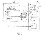
- Fig. 1 is a block diagram indicating the basic structure of an embodiment of this invention.
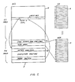
- Fig. 2 is a detail profile of
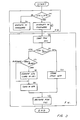
firmware part 5 of Fig. 1. - Fig. 3 is a flow chart indicating firmware processing.
- Fig. 1 illustrates basic structure of a embodiment of this invention. In this Figure, 1 is an instruction
control part unit 1 in a central processing unit CPU. 2 is an instruction register. 3 is a decoder which detects LCTL and SCTL instructions. 4 is an interrupt generating circuit. 5 is a particular instruction execution firmware routine FW. 6 indicates control registers CR provided in the CPU. 7 indicates control registers WCR defined on memory. 8 is a memory MS. The CPU comprises also an E (execution) unit which executes operation by receiving control information from the I unit, and an S unit which controls interfacing between the I unit, the E unit and MS. Those units can be replaced with others, as used in well-known computer systems, are not important to the present invention, and thus are not described. - In general, an instruction consists of an operation code field OP, a register designation field RR and a field for designating a memory address MA, etc.
- Instructions relating to control registers include LCTL and SCTL instructions.
- LCTL is an instruction to load the contents of a memory address designated by the MA field of the instruction into the control register designated by the RR field.
- On the other hand, SCTL is an instruction to store the contents of the control register designated by the RR field of the instruction into the memory address designated by the MA field.
- In addition to these instructions (LCTL, SCTL), there are provided:-
- an instruction for making reference only to a control register and executing specified processing, and
- an instruction for sending or receiving data between a general purpose register (not shown) in CPU and a control register.
- Program execution modes include an OS mode in which an ordinary instruction is executed directly by the hardware and micro-program, and a firmware mode in which special instructions (which cannot be executed by the hardware or micro-program) are executed by routines formed by combination of ordinary instructions.
- The LCTL, SCTL instructions are ordinary instructions which can be executed in the OS mode but these are executed in the firmware mode in this invention.
- Fig. 2 indicates the internal structure of
firmware 5 shown in Fig. 1. - An example of processing in accordance with LCTL and SCTL instructions is explained hereunder.
- When the
decoder 3 of the I unit detects an LCTL instruction under the OS mode, the instruction is not executed and an interrupt to thefirmware 5 is generated by theinterrupt generating circuit 4. At this time, in theinterrupt generating circuit 4, data such as a program status word PSW and an interrupt code, which indicates the cause of the interrupt, is stored in afirmware FW region 51 so that initial processing can be continued after execution offirmward routine 5 refer to Fig. 3), and the program execution mode is changed from the OS mode to the firmware mode (hereinafter called the FW mode). An interruptanalysis processing step 52 in thefirmware 5 analyses the interruption and starts execution of the LCTL instruction after recognizing that the interrupt was generated by (caused by) the LCTL instruction. - First, the firmward generates an LCTL instruction which is the same as the LCTL instruction mentioned above. Thereby, (1) (see Fig. 1) the contents to be loaded are written into the designated register among the control registers CRO to CR15 existing in the hardware. Here, if a control register CR not actually existing in the hardware is designated, entry into the register is not, of course, carried out, but the instruction itself is normally executed. However, @ (see Fig. 1) if a hardware control register which is required to be used simultaneously for two purposes is designated, loading into the control register (CR) is inhibited. When contents are required to be loaded to this control register (CR), the loading is carried out by using other instructions as an alternative to the LCTL instruction. For example, the instruction for loading the general purpose register from memory or the instruction for writing to the control register CR from the general purpose register.
- Then, ② ③' the contents of the address designated by the MA field of the LCTL instruction are written into the designated register among the control registers WCRO to WCR15 defined on the memory, by a MOVE instruction, and LCTL instruction execution is completed. Thereby, the contents of the CR and WCR registers become the same, except for the special control registers (to be used for two purposes) described above and control registers not existing in the hardware.
- Moreover, the PSW stored upon interruption is read from the region 51 (Fig. 2) in order to continue processing and the operation mode is returned to OS mode, from FW mode (refer to Fig. 3).
- As in the case of the LCTL instruction, when the
decoder 3 of the I unit detects the SCTL instruction, an interrupt is generated tofirmware 5 and the operation mode changes from OS mode to FW mode. in the SCTL instruction execution routine, @ (see Fig. 1) the contents of a designated register among the registers WCRO to WCR15 of theregister 7 defined on memory are written into anaddress 12 designated in the operand field of the SCTL instruction using a MOVE instruction, and thereby execution of the SCTL instruction is completed. At this time, since the latest control register contents are stored in registers WCRO to WCR15 defined on memory, it is not required to read data fromcontrol registers 6. - In addition, the PSW stored upon interruption is read from the
region 51, the operation mode is changed to OS mode from FW mode, and the instruction following the SCTL instruction is called. Thereby the processing is continued. - Fig. 3 is a flow chart indicating the above described firmware operations. First (a) each instruction in the OS mode is checked to determine if its instruction code is LCTL or SCTL. If it is neither, (b) it is processed by hardware (including processing by microinstructions). (c) If an instruction is either an LCTL or an SCTL instruction interruption to firmware is started. These operations are carried out by hardware or micro program.
- With the firmware started, first, (d) the processing required for saving PSW and an interrupt code is executed, (e) it is then determined whether the instruction is LCTL or SCTL. (f) When the instruction is an LCTL instruction, it is checked whether the control register designated is newly defined (NEW?) or to be used for another purpose (ALTERNATE?). This can be done by referring to the saved PSW or to a special control register. (g) When a control register designated is newly defined, the LCTL instruction to the register is here executed. When this instruction is detected under the firmward mode, it is immediately executed. This function is intrinsically provided in the hardware. Loading to the registers on the hardware terminates by execution of the LCTL instruction. Thereafter, (h) loading is also carried out to the control registers WCR defined on memory. In step (f), if an existing register is designated which is to be used for another purpose, processing moves to step (h), skipping step (g). Moreover, in step (e), when an instruction is an SCTL instruction, (i) data is stored from a register WCR using a MOVE instruction only.
- As explained above, 16 virtual registers in total are provided as WCRO to WCR15 and thereby the same content is loaded to both real and virtual control registers even when the real registers (CRO to CR15) exist. Therefore, it is no longer necessary to distinguish the real and virtual registers by checking register numbers and accordingly control can be realized easily.
Claims (4)
Applications Claiming Priority (2)
| Application Number | Priority Date | Filing Date | Title |
|---|---|---|---|
| JP57113470A JPS593642A (en) | 1982-06-30 | 1982-06-30 | Control register processing system |
| JP113470/82 | 1982-06-30 |
Publications (3)
| Publication Number | Publication Date |
|---|---|
| EP0098172A2 EP0098172A2 (en) | 1984-01-11 |
| EP0098172A3 EP0098172A3 (en) | 1985-10-09 |
| EP0098172B1 true EP0098172B1 (en) | 1989-05-10 |
Family
ID=14613061
Family Applications (1)
| Application Number | Title | Priority Date | Filing Date |
|---|---|---|---|
| EP83303789A Expired EP0098172B1 (en) | 1982-06-30 | 1983-06-30 | Register control processing system |
Country Status (9)
| Country | Link |
|---|---|
| US (1) | US4623962A (en) |
| EP (1) | EP0098172B1 (en) |
| JP (1) | JPS593642A (en) |
| KR (1) | KR890000100B1 (en) |
| AU (1) | AU546572B2 (en) |
| BR (1) | BR8303527A (en) |
| CA (1) | CA1200319A (en) |
| DE (1) | DE3379848D1 (en) |
| ES (1) | ES523751A0 (en) |
Cited By (1)
| Publication number | Priority date | Publication date | Assignee | Title |
|---|---|---|---|---|
| CN102037448B (en) * | 2008-05-23 | 2014-04-02 | Arm有限公司 | Device emulation support within a host data processing apparatus |
Families Citing this family (13)
| Publication number | Priority date | Publication date | Assignee | Title |
|---|---|---|---|---|
| JPS5960652A (en) * | 1982-09-30 | 1984-04-06 | Fujitsu Ltd | Data processing device |
| US5249266A (en) * | 1985-10-22 | 1993-09-28 | Texas Instruments Incorporated | Data processing apparatus with self-emulation capability |
| US5140687A (en) * | 1985-10-22 | 1992-08-18 | Texas Instruments Incorporated | Data processing apparatus with self-emulation capability |
| US5293631A (en) * | 1991-08-06 | 1994-03-08 | Hewlett-Packard Company | Analysis and optimization of array variables in compiler for instruction level parallel processor |
| US5666556A (en) * | 1993-12-30 | 1997-09-09 | Intel Corporation | Method and apparatus for redirecting register access requests wherein the register set is separate from a central processing unit |
| US5758117A (en) * | 1995-12-14 | 1998-05-26 | International Business Machines Corporation | Method and system for efficiently utilizing rename buffers to reduce dispatch unit stalls in a superscalar processor |
| US6298435B1 (en) * | 1996-04-16 | 2001-10-02 | International Business Machines Corporation | Methods and apparatus for exploiting virtual buffers to increase instruction parallelism in a pipelined processor |
| US6003126A (en) * | 1997-07-01 | 1999-12-14 | International Business Machines | Special instruction register including allocation field utilized for temporary designation of physical registers as general registers |
| US9229745B2 (en) | 2012-09-12 | 2016-01-05 | International Business Machines Corporation | Identifying load-hit-store conflicts |
| US10592164B2 (en) | 2017-11-14 | 2020-03-17 | International Business Machines Corporation | Portions of configuration state registers in-memory |
| US10901738B2 (en) * | 2017-11-14 | 2021-01-26 | International Business Machines Corporation | Bulk store and load operations of configuration state registers |
| US10761983B2 (en) * | 2017-11-14 | 2020-09-01 | International Business Machines Corporation | Memory based configuration state registers |
| CN116226021B (en) * | 2023-05-06 | 2023-07-25 | 摩尔线程智能科技(北京)有限责任公司 | Data receiving and transmitting method and device and graphics processor |
Family Cites Families (2)
| Publication number | Priority date | Publication date | Assignee | Title |
|---|---|---|---|---|
| US4351024A (en) * | 1975-04-21 | 1982-09-21 | Honeywell Information Systems Inc. | Switch system base mechanism |
| JPS5439539A (en) * | 1977-09-05 | 1979-03-27 | Hitachi Ltd | Data processor |
-
1982
- 1982-06-30 JP JP57113470A patent/JPS593642A/en active Granted
-
1983
- 1983-06-28 KR KR1019830002921A patent/KR890000100B1/en not_active IP Right Cessation
- 1983-06-29 CA CA000431511A patent/CA1200319A/en not_active Expired
- 1983-06-30 AU AU16409/83A patent/AU546572B2/en not_active Ceased
- 1983-06-30 BR BR8303527A patent/BR8303527A/en not_active IP Right Cessation
- 1983-06-30 US US06/509,609 patent/US4623962A/en not_active Expired - Fee Related
- 1983-06-30 EP EP83303789A patent/EP0098172B1/en not_active Expired
- 1983-06-30 ES ES523751A patent/ES523751A0/en active Granted
- 1983-06-30 DE DE8383303789T patent/DE3379848D1/en not_active Expired
Cited By (1)
| Publication number | Priority date | Publication date | Assignee | Title |
|---|---|---|---|---|
| CN102037448B (en) * | 2008-05-23 | 2014-04-02 | Arm有限公司 | Device emulation support within a host data processing apparatus |
Also Published As
| Publication number | Publication date |
|---|---|
| DE3379848D1 (en) | 1989-06-15 |
| BR8303527A (en) | 1984-02-07 |
| JPS593642A (en) | 1984-01-10 |
| JPH0517577B2 (en) | 1993-03-09 |
| CA1200319A (en) | 1986-02-04 |
| ES8405176A1 (en) | 1984-05-16 |
| AU1640983A (en) | 1984-01-05 |
| KR890000100B1 (en) | 1989-03-07 |
| US4623962A (en) | 1986-11-18 |
| EP0098172A3 (en) | 1985-10-09 |
| EP0098172A2 (en) | 1984-01-11 |
| ES523751A0 (en) | 1984-05-16 |
| AU546572B2 (en) | 1985-09-05 |
Similar Documents
| Publication | Publication Date | Title |
|---|---|---|
| US4434464A (en) | Memory protection system for effecting alteration of protection information without intervention of control program | |
| US4053752A (en) | Error recovery and control in a mass storage system | |
| US4975836A (en) | Virtual computer system | |
| EP0098172B1 (en) | Register control processing system | |
| US4679140A (en) | Data processor with control of the significant bit lengths of general purpose registers | |
| US4794522A (en) | Method for detecting modified object code in an emulator | |
| US5038281A (en) | Acceleration of system interrupts between operating systems in guest-host relationship | |
| EP0155211A2 (en) | System for by-pass control in pipeline operation of computer | |
| US4020471A (en) | Interrupt scan and processing system for a data processing system | |
| JPH0114611B2 (en) | ||
| US5325496A (en) | Selectable pointer validation in a computer system | |
| EP0202421A2 (en) | Batch file processing | |
| US5146586A (en) | Arrangement for storing an execution history in an information processing unit | |
| EP0290942B1 (en) | Guest machine execution control system for virtual machine system | |
| US4816992A (en) | Method of operating a data processing system in response to an interrupt | |
| CA1302582C (en) | Apparatus and method for control of asynchronous program interrupt events in a data processing system | |
| JPH0258648B2 (en) | ||
| JPS63120336A (en) | Switching system for memory access mode | |
| JPH0438011B2 (en) | ||
| JPS63103330A (en) | Detecting system for misuse of address stack | |
| JPH0535499A (en) | Data processing device and method | |
| JPS6227421B2 (en) | ||
| JPH03168845A (en) | Instruction execution control system | |
| JPS62154166A (en) | Microcomputer | |
| JPS6138508B2 (en) |
Legal Events
| Date | Code | Title | Description |
|---|---|---|---|
| PUAI | Public reference made under article 153(3) epc to a published international application that has entered the european phase |
Free format text: ORIGINAL CODE: 0009012 |
|
| AK | Designated contracting states |
Designated state(s): DE FR GB |
|
| PUAL | Search report despatched |
Free format text: ORIGINAL CODE: 0009013 |
|
| AK | Designated contracting states |
Designated state(s): DE FR GB |
|
| 17P | Request for examination filed |
Effective date: 19851204 |
|
| 17Q | First examination report despatched |
Effective date: 19861216 |
|
| GRAA | (expected) grant |
Free format text: ORIGINAL CODE: 0009210 |
|
| AK | Designated contracting states |
Kind code of ref document: B1 Designated state(s): DE FR GB |
|
| REF | Corresponds to: |
Ref document number: 3379848 Country of ref document: DE Date of ref document: 19890615 |
|
| ET | Fr: translation filed | ||
| PLBE | No opposition filed within time limit |
Free format text: ORIGINAL CODE: 0009261 |
|
| STAA | Information on the status of an ep patent application or granted ep patent |
Free format text: STATUS: NO OPPOSITION FILED WITHIN TIME LIMIT |
|
| 26N | No opposition filed | ||
| PGFP | Annual fee paid to national office [announced via postgrant information from national office to epo] |
Ref country code: FR Payment date: 19960611 Year of fee payment: 14 |
|
| PGFP | Annual fee paid to national office [announced via postgrant information from national office to epo] |
Ref country code: GB Payment date: 19960621 Year of fee payment: 14 |
|
| PGFP | Annual fee paid to national office [announced via postgrant information from national office to epo] |
Ref country code: DE Payment date: 19960627 Year of fee payment: 14 |
|
| PG25 | Lapsed in a contracting state [announced via postgrant information from national office to epo] |
Ref country code: GB Free format text: LAPSE BECAUSE OF NON-PAYMENT OF DUE FEES Effective date: 19970630 |
|
| GBPC | Gb: european patent ceased through non-payment of renewal fee |
Effective date: 19970630 |
|
| PG25 | Lapsed in a contracting state [announced via postgrant information from national office to epo] |
Ref country code: FR Free format text: LAPSE BECAUSE OF NON-PAYMENT OF DUE FEES Effective date: 19980227 |
|
| PG25 | Lapsed in a contracting state [announced via postgrant information from national office to epo] |
Ref country code: DE Free format text: LAPSE BECAUSE OF NON-PAYMENT OF DUE FEES Effective date: 19980303 |
|
| REG | Reference to a national code |
Ref country code: FR Ref legal event code: ST |
|
| REG | Reference to a national code |
Ref country code: FR Ref legal event code: ST |