EP0094869A1 - Verkapselungsgehäuse für mikroelektronische Schaltung mit hoher Wärmeabfuhr, und Verfahren zur Herstellung desselben - Google Patents
Verkapselungsgehäuse für mikroelektronische Schaltung mit hoher Wärmeabfuhr, und Verfahren zur Herstellung desselben Download PDFInfo
- Publication number
- EP0094869A1 EP0094869A1 EP83400928A EP83400928A EP0094869A1 EP 0094869 A1 EP0094869 A1 EP 0094869A1 EP 83400928 A EP83400928 A EP 83400928A EP 83400928 A EP83400928 A EP 83400928A EP 0094869 A1 EP0094869 A1 EP 0094869A1
- Authority
- EP
- European Patent Office
- Prior art keywords
- case
- frame
- solder
- microelectronic circuit
- manufacturing
- Prior art date
- Legal status (The legal status is an assumption and is not a legal conclusion. Google has not performed a legal analysis and makes no representation as to the accuracy of the status listed.)
- Granted
Links
Images
Classifications
-
- H—ELECTRICITY
- H01—ELECTRIC ELEMENTS
- H01L—SEMICONDUCTOR DEVICES NOT COVERED BY CLASS H10
- H01L23/00—Details of semiconductor or other solid state devices
- H01L23/02—Containers; Seals
- H01L23/10—Containers; Seals characterised by the material or arrangement of seals between parts, e.g. between cap and base of the container or between leads and walls of the container
-
- H—ELECTRICITY
- H01—ELECTRIC ELEMENTS
- H01L—SEMICONDUCTOR DEVICES NOT COVERED BY CLASS H10
- H01L21/00—Processes or apparatus adapted for the manufacture or treatment of semiconductor or solid state devices or of parts thereof
- H01L21/02—Manufacture or treatment of semiconductor devices or of parts thereof
- H01L21/04—Manufacture or treatment of semiconductor devices or of parts thereof the devices having at least one potential-jump barrier or surface barrier, e.g. PN junction, depletion layer or carrier concentration layer
- H01L21/50—Assembly of semiconductor devices using processes or apparatus not provided for in a single one of the subgroups H01L21/06 - H01L21/326, e.g. sealing of a cap to a base of a container
-
- H—ELECTRICITY
- H01—ELECTRIC ELEMENTS
- H01L—SEMICONDUCTOR DEVICES NOT COVERED BY CLASS H10
- H01L23/00—Details of semiconductor or other solid state devices
- H01L23/02—Containers; Seals
- H01L23/04—Containers; Seals characterised by the shape of the container or parts, e.g. caps, walls
- H01L23/043—Containers; Seals characterised by the shape of the container or parts, e.g. caps, walls the container being a hollow construction and having a conductive base as a mounting as well as a lead for the semiconductor body
- H01L23/047—Containers; Seals characterised by the shape of the container or parts, e.g. caps, walls the container being a hollow construction and having a conductive base as a mounting as well as a lead for the semiconductor body the other leads being parallel to the base
-
- H—ELECTRICITY
- H01—ELECTRIC ELEMENTS
- H01L—SEMICONDUCTOR DEVICES NOT COVERED BY CLASS H10
- H01L2924/00—Indexing scheme for arrangements or methods for connecting or disconnecting semiconductor or solid-state bodies as covered by H01L24/00
- H01L2924/0001—Technical content checked by a classifier
- H01L2924/0002—Not covered by any one of groups H01L24/00, H01L24/00 and H01L2224/00
Definitions
- the present invention relates to an encapsulation box for a hybrid circuit, with high heat dissipation, and external access connections crimped by glass beads.
- a case is provided with a metal bottom in order to dissipate the heat during the operation of the hybrid circuit.
- the invention also relates to the method for producing the case according to the invention.
- the hybrid circuits are produced on an insulating substrate, very generally of ceramic type, such as beryllium oxide or alumina.
- the environmental conditions imposed on hybrid circuits mean that they are frequently encapsulated in a metal case.
- the bottom of the case is a good thermal conductor and preferably made of copper.
- An encapsulation box whose bottom is made of copper is quite commonly produced by machining in a copper block.
- the external access connections sent in a metal tube are transferred by brazing the metal tube to the case, the copper being difficult to seal with a glass. This process is expensive.
- Another method consists in assembling by soft soldering a previously sent metal frame and a copper bottom.
- a soft solder can be incompatible with the solder used to add elements to the hybrid circuit.
- an encapsulation box of a hybrid power circuit, dissipating heat is constituted by a metal frame carrying the access connections fixed by glass beads, this frame being welded to the metal bottom of the preferably in copper by a high temperature solder, whose melting temperature is of the same order of magnitude, to within 100 °, as that of the glass for fixing the cones nexions.
- the invention relates to a microelectronic circuit encapsulation box with high heat dissipation, comprising a metal case bottom and good thermal conductor, a thick, metallic frame, crossed by a plurality of access connections exterior insulated by glass beads, this case being characterized in that the frame is fixed to the bottom of the case by means of a so-called high temperature solder whose melting range is within the softening temperature range of the glass sealing of external connections.
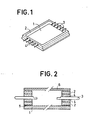
- FIG. 1 represents a model, among others, of a box for encapsulating hybrid circuits.
- the cover of the case has been removed so as to reveal its internal structure.
- the shape of the case is indifferent and can just as easily be square or rectangular.
- a hybrid power circuit encapsulation box includes a box bottom 1, and a frame 2 corresponding to the thickness of the hybrid circuit to be encapsulated. If the hybrid circuit dissipates power, it is then necessary that the hybrid circuit is produced on a thin ceramic plate so as not to oppose the heat transmission. The ceramic plate is then attached to a bottom of the case which is metallic and a good thermal conductor. Among the various possible metals, copper is the one which is preferred.
- Such a box can be produced in two different ways.
- a first method consists in machining in a sufficiently thick block of metal a cavity, so that a frame 2 appears secured to a bottom of case 1, since these two parts of the case are machined in the same block.
- a second method consists in cutting a bottom of case 1 in a plate of suitable thickness and in bringing on this bottom of case a frame 2, by appropriate means: this is the most commonly used method currently.
- Such a box necessarily includes external access connections 3. These can be added via insulating glass gaskets in the bottom of box 1, but this solution, although it belongs to the field of the invention , is not interesting: in fact, if the hybrid circuit considered gives off heat via the bottom of the case 1, this is preferably attached to a radiator or any other means for removing the dissipated heat. Consequently, the most logical and industrial solution consists in inserting the external access connections 3 into the frame. If the frame is ceramic there are no insulation problems between the external access connections 3, but on the other hand there are adaptation problems between the expansion coefficients of the bottom of the case 1 and of the frame 2: this is why the best possible adaptation consists in making an entirely metallic case, the bottom of the case, the frame, and the cover having similar expansion coefficients.
- a case bottom 1 and a frame 2 if they are respectively made of copper and steel for example, which is the preferred solution, can be welded to each other by means of a soft solder.
- the production of such a box requires two mounting operations: firstly the fixing of the external connections 3 in the frame 2 by means of glass beads 4, an operation which takes place at the melting temperature of the glass around from 800 to 900 ° C. Then the fixing by welding of the bottom of the case 1 on the frame 2 by a soft solder around 200 to 300 ° C depending on the alloy used.
- the invention consists in replacing the conventional soft solder with a high temperature solder, preferably chosen in such a way that the operations of mounting the frame on the bottom of the case and mounting the external connections in the glass beads are carried out simultaneously and in the same temperature zone.
- Figure 2 shows a sectional view of a housing according to the invention.
- This case consists of a bottom of case 1, metallic, and of a cover 6, also metallic, spaced apart by a frame which appears in section on the right and left parts of the figure.
- the frame 2 comprises a series of orifices in which are placed external access terminals 3, centered and insulated with respect to the metal frame 2 by glass powder, which, after sintering, gives the insulating glass beads 4.
- the welding of the frame 2 on the bottom of the case 1 is done by means of a high temperature solder 5 of the silver-manganese or silver-copper or gold-nickel type.
- the high temperature solder 5 can be, for example, a silver-copper alloy in the proportion of 72-28% which melts between 700 and 900 °, or a silver-manganese alloy in the proportion 85-15% which melts at a temperature greater than or equal to 900 ° C or an 82-18% gold-nickel alloy which melts at 950 ° C.
- the high temperature brazing alloy has a melting range which is within the viscosity range of the glass - in a pasty state, so both operations can take place simultaneously.
- the cover 6, which is also preferably metallic, can be attached to the frame 2 either by a conventional gold-tin preform, or by electrical welding.
Applications Claiming Priority (2)
| Application Number | Priority Date | Filing Date | Title |
|---|---|---|---|
| FR8207990A FR2526585A1 (fr) | 1982-05-07 | 1982-05-07 | Boitier d'encapsulation de circuit microelectronique a haute dissipation thermique et son procede de fabrication |
| FR8207990 | 1982-05-07 |
Publications (2)
| Publication Number | Publication Date |
|---|---|
| EP0094869A1 true EP0094869A1 (de) | 1983-11-23 |
| EP0094869B1 EP0094869B1 (de) | 1985-11-13 |
Family
ID=9273834
Family Applications (1)
| Application Number | Title | Priority Date | Filing Date |
|---|---|---|---|
| EP19830400928 Expired EP0094869B1 (de) | 1982-05-07 | 1983-05-06 | Verkapselungsgehäuse für mikroelektronische Schaltung mit hoher Wärmeabfuhr, und Verfahren zur Herstellung desselben |
Country Status (3)
| Country | Link |
|---|---|
| EP (1) | EP0094869B1 (de) |
| DE (1) | DE3361210D1 (de) |
| FR (1) | FR2526585A1 (de) |
Cited By (4)
| Publication number | Priority date | Publication date | Assignee | Title |
|---|---|---|---|---|
| FR2564243A1 (fr) * | 1984-05-11 | 1985-11-15 | Europ Composants Electron | Boitier a dissipation thermique d'encapsulation de circuits electriques |
| EP0233824A2 (de) * | 1986-02-19 | 1987-08-26 | Isotronics, Inc. | Gehäuse für Mikroschaltungen |
| FR2689681A1 (fr) * | 1992-04-07 | 1993-10-08 | Sept Doloy Sa | Réalisation par assemblage-brasage de boîtiers à plusieurs compartiments pour encapsulation de circuits microélectroniques. |
| WO2004073013A2 (de) * | 2003-02-13 | 2004-08-26 | Infineon Technologies Ag | Elektronisches bauteil mit halbleiterchip und verfahren zur herstellung desselben |
Families Citing this family (1)
| Publication number | Priority date | Publication date | Assignee | Title |
|---|---|---|---|---|
| DE3616969A1 (de) * | 1986-05-20 | 1987-11-26 | Bosch Gmbh Robert | Gehaeuse fuer integrierte schaltkreise |
Citations (1)
| Publication number | Priority date | Publication date | Assignee | Title |
|---|---|---|---|---|
| FR2436497A1 (fr) * | 1978-09-14 | 1980-04-11 | Isotronics Inc | Boitier plat entierement metallique possedant d'excellentes caracteristiques de transfert thermique |
-
1982
- 1982-05-07 FR FR8207990A patent/FR2526585A1/fr active Granted
-
1983
- 1983-05-06 DE DE8383400928T patent/DE3361210D1/de not_active Expired
- 1983-05-06 EP EP19830400928 patent/EP0094869B1/de not_active Expired
Patent Citations (1)
| Publication number | Priority date | Publication date | Assignee | Title |
|---|---|---|---|---|
| FR2436497A1 (fr) * | 1978-09-14 | 1980-04-11 | Isotronics Inc | Boitier plat entierement metallique possedant d'excellentes caracteristiques de transfert thermique |
Cited By (9)
| Publication number | Priority date | Publication date | Assignee | Title |
|---|---|---|---|---|
| FR2564243A1 (fr) * | 1984-05-11 | 1985-11-15 | Europ Composants Electron | Boitier a dissipation thermique d'encapsulation de circuits electriques |
| EP0165829A1 (de) * | 1984-05-11 | 1985-12-27 | Xeram | Verkapselungsgehäuse mit Wärmezerstreuung für elektrische Schaltungen |
| US4680673A (en) * | 1984-05-11 | 1987-07-14 | Societe Xeram | Encapsulated housing for dissipating heat produced by electrical circuits |
| EP0233824A2 (de) * | 1986-02-19 | 1987-08-26 | Isotronics, Inc. | Gehäuse für Mikroschaltungen |
| EP0233824A3 (de) * | 1986-02-19 | 1989-06-14 | Isotronics, Inc. | Gehäuse für Mikroschaltungen |
| FR2689681A1 (fr) * | 1992-04-07 | 1993-10-08 | Sept Doloy Sa | Réalisation par assemblage-brasage de boîtiers à plusieurs compartiments pour encapsulation de circuits microélectroniques. |
| WO2004073013A2 (de) * | 2003-02-13 | 2004-08-26 | Infineon Technologies Ag | Elektronisches bauteil mit halbleiterchip und verfahren zur herstellung desselben |
| WO2004073013A3 (de) * | 2003-02-13 | 2004-10-14 | Infineon Technologies Ag | Elektronisches bauteil mit halbleiterchip und verfahren zur herstellung desselben |
| US7622802B2 (en) | 2003-02-13 | 2009-11-24 | Infineon Technologies Ag | Electronic device with semiconductor chip including a radiofrequency power module |
Also Published As
| Publication number | Publication date |
|---|---|
| DE3361210D1 (en) | 1985-12-19 |
| FR2526585A1 (fr) | 1983-11-10 |
| EP0094869B1 (de) | 1985-11-13 |
| FR2526585B1 (de) | 1984-09-14 |
Similar Documents
| Publication | Publication Date | Title |
|---|---|---|
| EP0306412B1 (de) | Gehäuse für elektronische Schaltung | |
| FR2525815A1 (fr) | Substrat composite a haute conduction thermique et application aux boitiers de dispositifs semi-conducteurs | |
| US6111198A (en) | Duplex feedthrough and method therefor | |
| FR2518811A1 (fr) | Dispositif a circuit integre en conteneur de ceramique | |
| EP0037301B1 (de) | Verkapselungsgehäuse für Leistungsmodul in Hybridschaltung | |
| EP0094869B1 (de) | Verkapselungsgehäuse für mikroelektronische Schaltung mit hoher Wärmeabfuhr, und Verfahren zur Herstellung desselben | |
| EP0226480A1 (de) | Verfahren zur Herstellung eines Mikrogehäuses mit Kontaktflecken und dessen Anwendung für Karten mit elektronischen Bauelementen | |
| US5942796A (en) | Package structure for high-power surface-mounted electronic devices | |
| EP0114760B1 (de) | Gehäuse mit hoher Wärmeableitung, besonders für die Mikroelektronik | |
| CA1216960A (en) | Hermetic power chip packages | |
| EP0779775B1 (de) | Elektronische Baugruppe mit Wärmeabführung, besonders für Hochspannungsumwandler einer Entladungslampe von Scheinwerfer | |
| FR2833802A1 (fr) | Module de puissance et ensemble de modules de puissance | |
| FR2788376A1 (fr) | Boitier pour element photosemi-conducteur | |
| US5036584A (en) | Method of manufacture of copper cored enclosures for hybrid circuits | |
| JPH06120634A (ja) | セラミックス基板のスルーホール構造およびスルーホールセラミックス基板の製造方法 | |
| EP1035573A1 (de) | Elektrisches Leistungsbauelement auf einen Träger gelötet und Montierungsverfahren dafür | |
| EP1079432A1 (de) | Elektronisches Modul und Herstellungsverfahren eines solchen Moduls | |
| FR2706139A1 (fr) | Matériau pour brasure. | |
| JP4116809B2 (ja) | 熱電素子モジュールならびに半導体素子収納用パッケージおよび半導体モジュール | |
| US6600223B2 (en) | Hermetically sealing enclosure for housing photo-semiconductor devices and photo-semiconductor module incorporating the enclosure | |
| US5097245A (en) | Sub-miniature electrical component, particularly a fuse | |
| EP4062447B1 (de) | Metallischer leitender rahmen für elektronisches leistungmodul und zugehöriges herstellungsverfahren | |
| FR2523397A1 (fr) | Procede de montage de composants electroniques sur un support et produit realisable par le procede | |
| JP3457906B2 (ja) | 光半導体素子収納用パッケージ | |
| EP0065443A1 (de) | Verkapselungsgehäuse für Leistungshalbleiter funktionierend in einem Frequenzbereich von 2 bis 20 GHz |
Legal Events
| Date | Code | Title | Description |
|---|---|---|---|
| PUAI | Public reference made under article 153(3) epc to a published international application that has entered the european phase |
Free format text: ORIGINAL CODE: 0009012 |
|
| AK | Designated contracting states |
Designated state(s): DE GB IT |
|
| 17P | Request for examination filed |
Effective date: 19831203 |
|
| ITF | It: translation for a ep patent filed |
Owner name: JACOBACCI & PERANI S.P.A. |
|
| GRAA | (expected) grant |
Free format text: ORIGINAL CODE: 0009210 |
|
| AK | Designated contracting states |
Designated state(s): DE GB IT |
|
| REF | Corresponds to: |
Ref document number: 3361210 Country of ref document: DE Date of ref document: 19851219 |
|
| PLBE | No opposition filed within time limit |
Free format text: ORIGINAL CODE: 0009261 |
|
| STAA | Information on the status of an ep patent application or granted ep patent |
Free format text: STATUS: NO OPPOSITION FILED WITHIN TIME LIMIT |
|
| 26N | No opposition filed | ||
| ITTA | It: last paid annual fee | ||
| PGFP | Annual fee paid to national office [announced via postgrant information from national office to epo] |
Ref country code: GB Payment date: 19970416 Year of fee payment: 15 |
|
| PGFP | Annual fee paid to national office [announced via postgrant information from national office to epo] |
Ref country code: DE Payment date: 19970417 Year of fee payment: 15 |
|
| PG25 | Lapsed in a contracting state [announced via postgrant information from national office to epo] |
Ref country code: GB Free format text: LAPSE BECAUSE OF NON-PAYMENT OF DUE FEES Effective date: 19980506 |
|
| GBPC | Gb: european patent ceased through non-payment of renewal fee |
Effective date: 19980506 |
|
| PG25 | Lapsed in a contracting state [announced via postgrant information from national office to epo] |
Ref country code: DE Free format text: LAPSE BECAUSE OF NON-PAYMENT OF DUE FEES Effective date: 19990302 |