EP0094800A2 - Production control system, especially for garment manufacture - Google Patents
Production control system, especially for garment manufacture Download PDFInfo
- Publication number
- EP0094800A2 EP0094800A2 EP83302705A EP83302705A EP0094800A2 EP 0094800 A2 EP0094800 A2 EP 0094800A2 EP 83302705 A EP83302705 A EP 83302705A EP 83302705 A EP83302705 A EP 83302705A EP 0094800 A2 EP0094800 A2 EP 0094800A2
- Authority
- EP
- European Patent Office
- Prior art keywords
- oid
- data
- microsequencer
- card
- microcomputer
- Prior art date
- Legal status (The legal status is an assumption and is not a legal conclusion. Google has not performed a legal analysis and makes no representation as to the accuracy of the status listed.)
- Granted
Links
Images


Classifications
-
- G—PHYSICS
- G06—COMPUTING; CALCULATING OR COUNTING
- G06Q—INFORMATION AND COMMUNICATION TECHNOLOGY [ICT] SPECIALLY ADAPTED FOR ADMINISTRATIVE, COMMERCIAL, FINANCIAL, MANAGERIAL OR SUPERVISORY PURPOSES; SYSTEMS OR METHODS SPECIALLY ADAPTED FOR ADMINISTRATIVE, COMMERCIAL, FINANCIAL, MANAGERIAL OR SUPERVISORY PURPOSES, NOT OTHERWISE PROVIDED FOR
- G06Q10/00—Administration; Management
- G06Q10/06—Resources, workflows, human or project management; Enterprise or organisation planning; Enterprise or organisation modelling
-
- G—PHYSICS
- G05—CONTROLLING; REGULATING
- G05B—CONTROL OR REGULATING SYSTEMS IN GENERAL; FUNCTIONAL ELEMENTS OF SUCH SYSTEMS; MONITORING OR TESTING ARRANGEMENTS FOR SUCH SYSTEMS OR ELEMENTS
- G05B19/00—Programme-control systems
- G05B19/02—Programme-control systems electric
- G05B19/418—Total factory control, i.e. centrally controlling a plurality of machines, e.g. direct or distributed numerical control [DNC], flexible manufacturing systems [FMS], integrated manufacturing systems [IMS], computer integrated manufacturing [CIM]
- G05B19/4183—Total factory control, i.e. centrally controlling a plurality of machines, e.g. direct or distributed numerical control [DNC], flexible manufacturing systems [FMS], integrated manufacturing systems [IMS], computer integrated manufacturing [CIM] characterised by data acquisition, e.g. workpiece identification
-
- G—PHYSICS
- G07—CHECKING-DEVICES
- G07C—TIME OR ATTENDANCE REGISTERS; REGISTERING OR INDICATING THE WORKING OF MACHINES; GENERATING RANDOM NUMBERS; VOTING OR LOTTERY APPARATUS; ARRANGEMENTS, SYSTEMS OR APPARATUS FOR CHECKING NOT PROVIDED FOR ELSEWHERE
- G07C3/00—Registering or indicating the condition or the working of machines or other apparatus, other than vehicles
- G07C3/08—Registering or indicating the production of the machine either with or without registering working or idle time
- G07C3/10—Registering or indicating the production of the machine either with or without registering working or idle time using counting means
-
- Y—GENERAL TAGGING OF NEW TECHNOLOGICAL DEVELOPMENTS; GENERAL TAGGING OF CROSS-SECTIONAL TECHNOLOGIES SPANNING OVER SEVERAL SECTIONS OF THE IPC; TECHNICAL SUBJECTS COVERED BY FORMER USPC CROSS-REFERENCE ART COLLECTIONS [XRACs] AND DIGESTS
- Y02—TECHNOLOGIES OR APPLICATIONS FOR MITIGATION OR ADAPTATION AGAINST CLIMATE CHANGE
- Y02P—CLIMATE CHANGE MITIGATION TECHNOLOGIES IN THE PRODUCTION OR PROCESSING OF GOODS
- Y02P90/00—Enabling technologies with a potential contribution to greenhouse gas [GHG] emissions mitigation
- Y02P90/02—Total factory control, e.g. smart factories, flexible manufacturing systems [FMS] or integrated manufacturing systems [IMS]
Definitions
- This invention relates to a production control system for on-line control of factory operations and, in particular but not exclusively, to the control of various functions in a garment manufacturing factory.
- One object therefor of the production control system disclosed herein is to provide real-time control of major functions in a garment manufacturing factory, such as production planning, production scheduling, factory loading, factory progress control, section/line balancing, work-in-progress level control, and gross payroll and labour cost control.
- major functions in a garment manufacturing factory such as production planning, production scheduling, factory loading, factory progress control, section/line balancing, work-in-progress level control, and gross payroll and labour cost control.
- the aim of the on-line production control system now to be disclosed herein is to achieve up-to-the-minute control of manufacturing operations so that corrective action can be taken to prevent potential problems occuring in the future.
- a production or work control system for a works environment comprising a multiplicity of operator input devices (OIDs) situated at the work stations of human operatives and each having a card reader; and a multiplexor/concentrator consisting of the canbination of a microcomputer and a microprocessor, the microprocessor comprising a microsequencer repeatedly scanning the OIDs in a continuous operation to acquire data therefran which is passed to the microcomputer, the microcomputer carrying out validity checking on the data input from the OIDs by the microsequencer storing good data in short-term store and returning to the microsequencer signals indicative of the validity or otherwise of each data input consequent upon a card reading at an OID, the microsequencer returning to the individual OIDs the signals indicative of the validity or otherwise of their data inputs, and the microcomputer having input and output ports for communication with a host computer, such as a minicomputer.
- OIDs operator input devices
- the microprocessor/microsequencer may be a bipolar bit-slice microprocessor of the single-level pipelined type driven by writeable microcode.
- the microcomputer may be a Z80 computer board.
- an operator input device for use in a system of production or work control, comprising a card reader for scanning a card or ticket bearing encoded data when said card is placed in the card reader and generating electrical signals representative of said encoded data, a cable for supplying low-voltage external electrical power to the OID over a pair of electrical lines, pulse train-generating-circuitry responsive to the card reader output signals to derive a stream of pulses of at least two different durations representing the encoded data, said pulse train-generating-circuitry taking its electrical supply from said pair of lines, and short-circuiting means powered from said pair of lines and responsive to said stream of pulses to substantially short together said lines for a succession of time periods corresponding to the time durations of said pulses, whereby the data from the card or ticket is transmitted by the OID on the same cable pair as supplies the OID with its electrical power.
- OID operator input device
- the short-circuiting means may be driven by an optical isolator having a radiation emitter to which said stream of pulses is applied, and a receiver responsive to the radiation from said emitter and electrically isolated therefrom, such as by diodes.
- each card or ticket bears two parallel bar code tracks, the first being a clock track of regularly spaced thin bars, and the second a data track having either a thick bar or a space opposite each thin bar bit of the clock track to indicate 'ones' and 'zeros', and the scanning means comprises a first emitter/receiver combination scanning the clock track and a second emitter/receiver combination scanning the data track.
- the OID includes two monostable circuits having different time periods to generate pulses of different widths, and logic circuitry responsive to the signals from the receivers of the scanning emitter/receivers to direct each clock bit to the triggering input of one or other of the monostable circuits according to whether the data track is simultaneously showing a bar or a space.
- the outputs of the two monostable circuits are gated together to provide the stream of pulses that is applied to the transistor feeding the light-emitting diode of the optical isolator.
- the OID further comprises audio and/or visual response means which is energized by the external power supply cable when the polarity of the voltage on the cable line pair is reversed.
- communication between the MUXC and a host minicomputer is established over a serial link including optical isolating devices. Power is transferred via a transformer.
- the system can load the factory with an optimum style mix to maintain targetted production levels, whilst meeting customer delivery requirements.
- the level of work-in-progress can be maintained at the level required for efficient factory operation, and production orders can be systematically progressed so that they emerge completed into the warehouse in the minimum throughput time.
- An OID is mounted at each human operative's workplace and is used to read bar-coded operator cards, operation cards, and bundle cards submitted by the operative.
- Each OID is connected to a data concentrator or multiplexor (MPX), which is microcomputer controlled.
- MPX performs certain checks on data fed in from the OID's, and then transmits the data for processing to the central computer system, which may comprise a Minicomputer system, e.g. a Hewlett-Packard HP1000, with central processor, disk drive, visual display unit(s), printer and optional nagnetic tape back-up.
- Minicomputer system e.g. a Hewlett-Packard HP1000, with central processor, disk drive, visual display unit(s), printer and optional nagnetic tape back-up.
- Each human supervisor may have a terminal comprising a small visual display unit, which is connected to the central computer system and is used to input information to, or request data from, the computer.
- the OID enables each operative to clock in and out, at the beginning and end of a day, thereby eliminating time wasting at traditional clocking stations.
- the operative also uses the device to notify the central computer of the operation currently being carried out and what job lot is currently being worked on. This enables the central computer to calculate gross payroll, fully automatically.
- the operative uses three kinds of card, a personal card with which he/she clocks in and out, an operation card, with which he/she indicates the operation he/she is performing, and a job lot card, which travels with each job lot through the factory and indicates on which job lot the operative is working.
- the supervisor terminal which is of the television type, has a keyboard by means of which the supervisor can call up information as to how much work each operative has done that day and at what rate he/she is working, also information as to where each job lot is in the factory, and information on how much work is waiting at each operator station, to enable the supervisor to balance the work flow through the factory much better. Also, on the screen, he/she can obtain accounting reports showing all off-standard work and operator down-time on his/her section, by operative, by time and by cost.
- the whole system is real time, which means that any time a supervisor enquires for information it is up to date.
- the system also allows for a whole series of problem types to trigger warning signals at the supervisor's terminal, such as production at a certain operation falling below the minimum rate per hour or a particular machine being broken down for more than a certain time or the pile of work at any particular station rising above a critical level.
- the operator input device is driven fran a multiplexor concentrator MUXC.
- the device reads optical bar-code produced elsewhere by software driving a standard HP2631B printer.
- the OID reads a bar data and clock track and sends the results to a MUXC.
- the MUXC communicates back the status of the read to the OID which in turn, by an audio/visual response, communicates to the operative.
- This device comprises two microprocessors (a microsequencer or bit slicer and a Z80 Computer board).
- a combination of microcode and firmware allows data from up to 128 OID's to be temporarily stored for up to eight hours in memory as back-up to the data being transferred to an HP1000E central computer where the data is permanently stored and updates a data base.
- the data base provides information in real-time to terminals on the shop floor.
- the data transfer between the MUXC and the central computer is via isolating adapter circuitry allowing RS423 protocol to interface with RS232 protocol.
- Data transfer between the MUXC and the OIDs, and power supply from the MUXC to the OIDs, is by a system of channels and sub-channels.
- Software for the above hardware includes the following.
- Microcode is provided for the microsequencer or bit slicer to enable it to scan the OIDs and respond to the data inputted fran the OIDs.
- the Z80 software includes a program for loading the microcode into the microsequencer and a main program enabling the Z80 to control the entire operation of the MUXC.
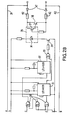
- FIG. 1 the operator input device ( Figure 1), this appears externally as a box 10 with a side reader 12 presenting a card-reading slot 11, green and red signal lamps 13, 14 in the form of light-emitting diodes being provided on the box front.
- a single twisted pair cable provides the link between the OID and the MUXC, carrying both data signals between the OID and the MUXC and a 24 volt power supply from the MUXC to the OID.
- the MUXC can sustain up to 128 OlDs.
- the OID box 10 contains a single printed circuit board.
- the OID itself has no ability to operate on the different types but merely detects and sends the detected signals to the MUXC.
- the green lamp 13 When the power is on, the green lamp 13 is lit and stays on constantly showing the OID is in working status.
- the data is read and passed to the MUXC where it is checked for three possible states. One of these states is returned to the OID where both an aural signal and a visual signal via the red lamp 14 are emitted.
- a single aural tone and a single red lamp pulse are caused to be emitted from the OID.
- the operative can then return to his/her work.
- the system is designed so that an operative (employee) identification and the type of work (operation) must have been input in that order before any work (job lot) ticket can be passed through the reader and be accepted, i.e.
- a physical error is caused by a misread of the characteristics on the input card (any type). This may be caused by damage to the card, incorrect method of slotting the card through the reader or malfunction of the OID, though this latter is designed such that should it physically malfunction the green lamp 13 will be extinguished. In case of a physical error, a series of eight short regular pulses will be given by the aural bleeper and the red lamp.
- the black to white contrast ratio on the bar card is detected by infra red detectors and converted to digital pulses of the correct width.
- the MUXC will respond back to the OID by sending a coded tone to identify a good read, or a physical or logical error.
- the MUXC channel to which the OID is connected holds one line A at +12 volts through a 120 ohn resistor and the other line B at -12 volts through another 120 ohm resistor. This is the normal state of the circuit; when the MUXC channel wishes to acknowledge some form of read, the polarity is reversed which energises the audible bleeper and lamp in the OID.
- the standing current is about 20 mA so that a voltage of about 18 volts is available at the OID terminals.
- the OID itself generates signals by shorting the lines together for very short periods. A zero bit is indicated by a 100 microsecond pulse and a one bit by a 300 microsecond pulse. In fact, the lines are pulled to within about 4 volts of each other rather than a dead short.
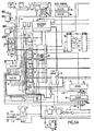
- the OID circuit is as follows.
- the voltage applied across input tenninals 15 (line A) and 16 (line B) is applied via line-isolating diodes 17 to a reservoir capacitor 18 which charges to about 16 volts (line less 2 diode drops).
- This supplies a 12 volt regulator 19 which powers the rest of the circuit, except for the audio unit 20 and red lamp 14 which during normal voltage on the terminals 15, 16 are isolated by diodes 21.
- a series chain includes a brightness-adjustment resistor 22 and three lED's, one of which is the green (ready) lamp 12 while the other two are infra-red LED's 23 which illuminate the clock and data tracks on the cards to be read.
- the data and clock tracks on a card, illuminated by respective LED's 23, are read by respective photo-transistors 26 the outputs of which are fed to respective identical circuits 24, 25.
- Each of the circuits 24, 25 canprises a cascode 27 and a MOSFET operational amplifier buffer 28.
- a resistor chain 29 provides bias to the cascodes and operational amplifiers of both circuits 24, 25.
- the operational amplifiers 28 have a high output for black bars on the card being read.
- the durations of the output bits of the OID are determined by a 300 microsecond monostable circuit 31 (one bit) and a 100 microsecond monostable circuit 32 (zero bit).
- a three-gate logic circuit 30 the clock track signal output of the circuit 25 is switched by the data track signal output of the circuit 24 either to the monostable 31 to generate a one bit (data black) or to the monostable 32 to generate a zero bit (data white).
- White-to-black transitions on the clock track thereby trigger one or other of the monostables 31, 32.
- the outputs of both monostables are combined into a single pulse train at an OR gate 33, the output of which is applied to the base of a drive transistor 34 which drives an opto-isolator 35.
- the opto-isolator 35 consists of a photo-diode 36, in series with the transistor 34, and a photo-transistor 37.
- An output transistor 38 in Darlington connection with the photo-transistor 37 effectively shorts the lines 39, 40 via isolating diodes 41 and damping resistors 42.
- Figure 3 shows a typical bar-coded card 43 to be read by the CPI.
- the clock track 44 and the data track 45 are immediately one below the other, the clock track consisting of a horizontal series of evenly spaced thin vertical bars while the data track consists of thick bars irregularly spaced.
- the clock track contains 60 OR-signs and the data track provides a cursor-sign under a corresponding clock pulse where the data bit is a one.
- the bottom edge 46 of the card is a zero reference, and the data and clock tracks are printed between 4 mm up from the bottan and 17 mn from the bottom.
- the bar code tracks are printed by the HP2631B printer on comparatively thin white flexible sheet so that each card is in the form of a ticket that can, if it is a job lot card for example, be readily stapled to the work.
- the cards can be printed on sheet that is a number of cards wide and separated afterwards by guillotining.
- Figure 4 shows the scanning arrangement of emitters and receivers in the reader 12 of the OID 10.
- the zero reference edge 46 of the card 43 rests on the horizontal upper edge 47 of a shim plate 48 in the lower part of the card reader slot 11.
- the card is moved horizontally through the reader slot 11 from back to front of the reader.
- the two infra-red LIDs 23 illuminate the clock track 44 and the data track 45, respectively, and the two photo-transistors 26 receive, respectively, the reflections from those tracks.
- the photo-transistors 26 are angled obliquely in order to provide adequate space, and the clock track 44 and the data track 45 are scanned through respective wedge-form transparent blocks 49, 50 separated by an opaque body 51, further opaque bodies 52, 53 being situated above and below the transparent blocks.
- the portion 54 of the body of the reader 12 that lies on the side of the slot 11 remote from the emitters 23 and receivers 26 is removable, and is both opaque and non-reflecting.
- the sixteen bits devoted to the parity and EOC bytes for the detection and correction of errors gives good protection of the data having regard to the nature of the cards and the usage to which they are put.
- the multiplexor/concentrator comprises two microprocessors, a Z80 board and a microsequencer.
- the Z80 computer board controls the entire operation of the network multiplexer and interfaces with the host HP1000E minicomputer via a serial link.
- the microsequencer is located physically and functionally between the Z80 microprocessor and the operator input devices and is a bipolar bit-slice microprocessor driven by writeable microcode which scans 128 sub-channels in an endless sequence servicing the OIDs and buffering data bidirectionally between them and the Z80.
- the 128 sub-channels are grouped in fours, with four such groups of four (16 sub-channels) being serviced by each of eight main channel boards that are in turn serviced by the microsequencer.
- the microsequencer ( Figures 5A and 5B) is based on Advanced Micro Devices 2900-series integrated circuits. In essence it is a standard AMD 2901 single-level-pipelined microprocessor.
- the microprogram is organised as a 256 word by 32 bit array and is stored in the first quarter of a 4 x MK4801 (Mostek 70 nanosecond lk x 8 bit static RAM) memory array 55.
- the direct branch can be modified by three S-bits in a status register 57 to give an eight-way branch dependent on the state of a sub-channel as received at 86.
- the microprogram word is decoded and is latched at the beginning of each clock cycle in various chips 58 - 64.
- a microword field is encoded (e.g. four 'data-in' paths encoded into bits 25/24)
- the decoder chip e.g. 61
- the latch e.g. 62
- the microwords designate either a Branch or an ALU (Arithmetic Logic Unit 74) instruction cycle according to the value in a 'data-out' (D-out) field (bits 28-26). If these bits are all ones (indicating a Branch instruction) the microprogram either branches or continues depending on:
- the branch address is taken from a D-field (7-0) in the microinstruction.
- the I-field (ALU instruction) is always zero (NJP) for Branches so that the AID does not alter any registers etc.
- the D-in field is immaterial for Branch instructions.
- bit 16 is always 'one'.
- the corresponding reduction of the I field from nine to eight bits results in a much more convenient arrangement for assigning the microword bits. If the I-field designates input from the D-inputs this is obtained from one of four sources as indicated by the D-in field (bits 25, 24). These are:
- the ALU 74 output is strobed into the destination designated by the D-out field as follows.
- the high-order three bits (31-29) of the microinstruction are latched in a 'Scope Trigger' register 68. This is for diagnostic trace purposes only.
- the clock is a standard 8MHz oscillator 69 followed by a binary divider 70 producing a 4MHz square-wave (the basic clock pulse). This feeds a delay line 71 with five 50 nanosecond taps, and decoders 72 produce three subsidiary clock pulses.
- these subsidiary clocks are as follows:
- a timer 75 is a free-running LM555 oscillator operating at about 16Hz. It is synchronised with the microsequencer scan by a circuit 76 and the microprogram so that the T-stat is 'one' for exactly one complete cycle every 1/16th of a second.
- a register 77 is connected to the address lines of the microcode array and four registers 78 (32 bits) to the data lines.
- Z80 software loads each of the five registers for each microword, finally strobing the array write line to write the word into the array.
- Ports A and B are the data and control/address ports for this operation. After microcode load bit 6 of port B is set zero which disconnects the above arrangement and establishes the normal pipelined data flow. Subsequently bit 7 of Port B is set zero which enables the clock pulses.
- a circuit 79 ensures that the microprogram starts cleanly at address zero.
- the port 81 addresses register 80 via register 85 for the routing in of Z80 data from port A.
- Register 82 is used in the routing of data out to Z80.
- Monostables 83 and 84 provide A and B strobe pulses for the timing of port A handshakes which are bidirectional.
- the program operates in an endless cycle scanning sub-channels O to 127 decimal.
- the board contains an eight byte work area for each sub-channel and this is initially formatted by the reset function.
- Each work area contains the current state, the current time-out value and the current byte and bit count for the sub-channel. All slots are initialised to
- the cycle starts at location zero.
- the sub-channel counter is incremented and the clock line (to channels) is activated. (If the sub-channel is zero this pulse is extended and the T-stat is set if this is a timer cycle).
- the state of the sub-channel is used to give an immediate branch to the entry point in the microcode for the current state.
- the sub-channels move individually through the states as follows.
- States 4 and 5 are exclusive to a single sub-channel at a time. All other states are shareable.
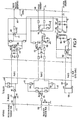
- Figure 6 shows the circuit of one of the eight channel boards that serve as interfaces between the microsequencer of Figures 5A and 5B and the Operator Input Devices (via the sub-channels).
- Each channel has its own unique channel address (bits 0-7), set on switches on the board, and can support up to sixteen sub-channels.
- Each sub-channel in turn supports one OID.
- the microsequencer controls the channel timing ( Figures 10A and 10B) via a backplane line (SYSCK/EC) inputting to the channel at 116.
- the microprogram causes this line to carry a stream of pulses each one occurring at the start of a sub-channel period. At the start of sub-channel zero's period this pulse, normally 750 nsec, is extended to 1500 nsec. Each full cycle is 128 sub-channels in length.
- a monostable 88 is fired producing a pulse of approx 150 nsec which is passed down a delay line 89 with 100 nsec taps.
- the original pulse and the first three delayed pulses are denoted T0, Tl, T2 and T3 respectively.
- a second monostable 90 (period 1100 nsec) is fired by the leading edge of the clock pulse and a seven-bit counter 91, 92, clocked at TO, is cleared if this monostable has timed-out and incremented if it has not. The effect is that the counters on all channels keep in step with the microsequencer.
- the high-order three bits of the seven-bit counter are compared in a comparator 93 with the address set by the address switches 94.
- An equal condition means that this channel is selected and this activates the sub-channel decoder 95, 96.
- the same signal is ANDed at 97 with T3 to provide the Channel Clear' (CHCLR) signal at 98.
- CHCLR Channel Clear'
- the sub-channel decoder 95, 96 drives one line per sub-channel to select the sub-channel according to the low-order four bits of the counter 91, 92.
- Line driver circuit 99 is simply a bilateral switch which in the normal condition (input low) holds line A to plus twelve volts via a 120 ohn resistor and line B to minus twelve volts via a 120 ohm resistor.
- line A is positive and line B negative and, due to the OID standing current of about 20mA, the actual voltages are about plus/ minus 9 volts.
- An operational amplifier 100 senses the line pair using a balanced differential input network 101 and its output, after clamping and filtering at 102, is logic zero at input 103 to a mnostable 104, in the normal line state.
- the contents of the flip-flops 107, 108 are applied to the internal buses 109 by gates 110.
- the DATA and READY flip-flops are cleared at T3 via gate 111 when the sub-channel is selected, i.e. imnediately after transfer of their contents to the canon DATA/READY circuits 112 of the parent channel board.
- the READY and DATA flip-flops 107, 108 of the selected sub-channel are clocked into the common DATA and READY flip-flops 113, 114 of the parent channel and these are applied via gates 115 to the backplane line returning to the microsequencer.
- the microsequencer can activate the 'line reverse' backplane line at 117 during a sub-channel cycle in order to activate the OID's red lamp and audio signal.
- the backplane BUS signal (LINE REVERSE/-EA) is received on the channel board and routed to input 118 of each sub-channel circuit to trigger monostable 119 in the selected sub-channel circuit. This monostable stretches the pulse out to approximately 1/16 second and activates the bilateral switch 99 to reverse the line AB polarity.
- the other input of the monostable 119 is driven by the sub-channel select line 120 so that only the correct sub-channel responds.
- the Z80 board which controls the operation of the network multiplexer is shown in Figures 8A to 8J. At initialisation it downloads the micro-code into the microsequencer and causes it to perform a total system reset. Thereafter, the Z80 board receives message blocks fran the microsequencer, checks them and sends back an appropriate acknowledgement code. Good blocks are stored in its 256K byte memory for transmission to the host computer via the serial link.
- the Z80 board is highly modular in design and layout.
- the board contains the following functional blocks:
- the ROM array 122 consists of eight sockets for 2716-type EPROMS 124. After reset this array is mapped into the first 16K byte quadrant of the Z80 address range. CPU execution starts at location zero. The board is designed on the assumption that the ROM program will copy all the operational code into the first 16K of RAM and will then transfer to it. The ROM loader does this by simultaneously switching the ROM off-line and the first 16K of RAM on-line using the parallel port controlling the memory map circuit. Thereafter the ROM is not accessible by the CPU and performs no further function. TIle ROM data output is buffered to reduce capacitative loading.
- This array is a standard arrangement of 4x8 64K dynamic RAM chips 123.
- the address bus to this array is eighteen bits wide and consists of three (high-order) bits from the mapping circuit plus the low-order fifteen bits of the Z80 address bus.
- This circuit is a standard 4MHz clock 125.
- the Wait State function 126 is to insert one wait state in all memory accesses while the ROM is enabled. This only occurs during initialisation time and is due to the slow access time of the ROM chips.
- the Reset circuit 127 is activated by power-on or external button. For this board there is no need to preserve RAM contents on reset so a very simple circuit suffices.
- the low-order four bits of the A port 136 of the Mapping PIO control this function. After reset these bits are all high.
- the Z80 sees the ROM array in the low-order quandrant of its address space and the RAM is disabled for any access to this or the next quadrant. It is intended that the ROM code will imnediately set bits 3-1 to zero (leaving bit 0 high) and in this state the low-order 32K field of the RAM appears in the high-order half of the Z80 address space. Now the ROM loader can copy all the code to the low-order 32K of the RAM where it will remain throughout normal running.
- the ROM loader When the ROM loader is finished it will write zero to bit O of the port and instantly remove the ROM memory (and the wait states) and map the RAM field into the low-order half of the Z80 address space.
- the Z80 simply continues executing instructions but they are now coming from the RAM. By storing the 3-bit address of one of the eight 32K RAM fields into bits 3-1 of the port the Z80 can access this field in the upper half of its address space.
- Standard Z80 CTC chip 130 Channels 2 to 3 cascaded to form a 1 second clock.
- Channel 0 provides the SIO bit rate clock at 16 times 9600 baud.
- a power circuit 133 using a charge pump produces plus/minus twelve volts for an RS232 interface.
- the SIO chip 131 provides two independent RS232 full duplex serial channels at 9600 baud.
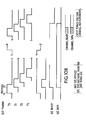
- the main Z80 program (Appendix III) consists, in essence, of a simple endless background loop, as shown in the flow sheets of Appendix IV, which interacts with five foreground interrupt routines.
- the Z80 input routine from the host operates as follows:
- the Z80 input routine fran the microsequencer works in exactly the same way with the following exceptions.
- the Z80 output routine to the host is the inverse of the host input routine described above.
- the background routine initiates the operation, sets the byte counter to 1 and the flag to 2 and outputs the first character to the SIO chip.
- the Z80 output routine to the microsequencer is similar to the host output except:
- the system has an HP1000 mini-computer at the center of a network of units with which it communicates via asynchronous serial links. These units will commonly have RS232 interfaces. RS232 interfaces are not rated for operation at distances greater than fifteen metres although, under favourable circumstances, they will sometimes function adequately up to three or four times that distance. However, in the factory environment for which the system is intended, and particularly in view of the intended operation data rate (9600 baud), these interfaces are considered inadequate.
- Figure 9 shows the electrical circuitry for a single channel.
- the terminal RS232 signal at 148 is buffered by an LF352 (JFET op-amp) circuit 149 which is differential and therefore provides better noise immunity than normal. Thereafter, the circuit is the same as that used by the OlD readers and consists of an opto-isolator 150 driven by a transistor 151 and with its photo-transistor 152 connected in a Darlington pair with a further transistor 153 that shorts line pair 2, drawing current symmetrically through two 120 ohm terminating resistors 154.
- the differential signal is decoded by a JFET op-amp circuit 155 which drives the RS232 receive data line 156. Since it is intended that there should be RS423 compatibility at this point the signal is clamped at 157 to approximately +/- 6 volts.
- Power is provided over the third pair of the 3-pair telephone cable to the remote interface box.
- This line pair is driven by a 12v DC source 158 grounded at the local end.
- the positive line is protected by a fuse 159.
- the supply is decoupled at the remote end by a reservoir capacitor 160 and supplies the primary side 165 of a trans- fonner 161.
- a CMOS oscillator 162 is set to run at approximately 50kHz and this signal switches the primary current in the transformer via a transistor 163.
- the centre-tapped fly-back voltage is clamped by a 20v Zener diode 164.
- the centre-tapped secondary coils 166 drive two rectifier/stabiliser circuits 167 which produce the local + and - 12v supply referred to the terminal ground.
- the total current available is of the order of 20mA which is more than required by the local circuits.
- the isolating adapter circuitry described is one of the factors that makes the system particularly suitable for a works environment. But there are numerous other features that contribute to this.
- the Operator Input Devices located at each work station are simple and inexpensive yet extremely robust, and the cards or tickets that they read are particularly cheap and easy to print. Yet the cards will withstand considerable abuse - a card that has been screwed up or torn can still nonnally be reflattened and successfully read.
- Each OID being parasitically supplied with power at a completely safe 24 volt level via its data transmission and control link, can be situated anywhere in the works.
- the MUXC receives data from the OlDs that gives a complete and up-to-date picture of work in hand in the factory, showing the progress of particular orders, detecting break downs and bottle necks, recording employee attendances and work rates, and generally providing all the information necessary to plan the meeting of delivery targets, use the available personnel and facilities in the most efficient manner, oversee the stock position, carry out payroll computations, and anticipate problems and take preventive action.
- the microcomputers of the MUXC are provided with electric battery power supply back-up to prevent failure in the event of a mains power interruption.
Abstract
Description
- This invention relates to a production control system for on-line control of factory operations and, in particular but not exclusively, to the control of various functions in a garment manufacturing factory.
- In today's operating conditions, clothing manufacturers need to maintain tight controls over both factory costs and their investment in stocks and work-in-progress, if their business is to survive. Whilst clothing companies have generally became much more complex to organise and operate over recent years, the tools provided to assist management and supervision in the control of factory operations have not changed dramatically.
- One object therefor of the production control system disclosed herein is to provide real-time control of major functions in a garment manufacturing factory, such as production planning, production scheduling, factory loading, factory progress control, section/line balancing, work-in-progress level control, and gross payroll and labour cost control. Whilst existing systems report historically on what happened in the factory yesterday, the aim of the on-line production control system now to be disclosed herein is to achieve up-to-the-minute control of manufacturing operations so that corrective action can be taken to prevent potential problems occuring in the future.
- According to one aspect of the present invention there is provided a production or work control system for a works environment, comprising a multiplicity of operator input devices (OIDs) situated at the work stations of human operatives and each having a card reader; and a multiplexor/concentrator consisting of the canbination of a microcomputer and a microprocessor, the microprocessor comprising a microsequencer repeatedly scanning the OIDs in a continuous operation to acquire data therefran which is passed to the microcomputer, the microcomputer carrying out validity checking on the data input from the OIDs by the microsequencer storing good data in short-term store and returning to the microsequencer signals indicative of the validity or otherwise of each data input consequent upon a card reading at an OID, the microsequencer returning to the individual OIDs the signals indicative of the validity or otherwise of their data inputs, and the microcomputer having input and output ports for communication with a host computer, such as a minicomputer.
- The microprocessor/microsequencer may be a bipolar bit-slice microprocessor of the single-level pipelined type driven by writeable microcode. The microcomputer may be a Z80 computer board.
- According to another aspect of the invention there is provided an operator input device (OID) for use in a system of production or work control, comprising a card reader for scanning a card or ticket bearing encoded data when said card is placed in the card reader and generating electrical signals representative of said encoded data, a cable for supplying low-voltage external electrical power to the OID over a pair of electrical lines, pulse train-generating-circuitry responsive to the card reader output signals to derive a stream of pulses of at least two different durations representing the encoded data, said pulse train-generating-circuitry taking its electrical supply from said pair of lines, and short-circuiting means powered from said pair of lines and responsive to said stream of pulses to substantially short together said lines for a succession of time periods corresponding to the time durations of said pulses, whereby the data from the card or ticket is transmitted by the OID on the same cable pair as supplies the OID with its electrical power.
- The short-circuiting means may be driven by an optical isolator having a radiation emitter to which said stream of pulses is applied, and a receiver responsive to the radiation from said emitter and electrically isolated therefrom, such as by diodes.
- In the preferred embodiment, each card or ticket bears two parallel bar code tracks, the first being a clock track of regularly spaced thin bars, and the second a data track having either a thick bar or a space opposite each thin bar bit of the clock track to indicate 'ones' and 'zeros', and the scanning means comprises a first emitter/receiver combination scanning the clock track and a second emitter/receiver combination scanning the data track. The OID includes two monostable circuits having different time periods to generate pulses of different widths, and logic circuitry responsive to the signals from the receivers of the scanning emitter/receivers to direct each clock bit to the triggering input of one or other of the monostable circuits according to whether the data track is simultaneously showing a bar or a space. The outputs of the two monostable circuits are gated together to provide the stream of pulses that is applied to the transistor feeding the light-emitting diode of the optical isolator. The OID further comprises audio and/or visual response means which is energized by the external power supply cable when the polarity of the voltage on the cable line pair is reversed.
- According to a further aspect, communication between the MUXC and a host minicomputer is established over a serial link including optical isolating devices. Power is transferred via a transformer.
- The system can load the factory with an optimum style mix to maintain targetted production levels, whilst meeting customer delivery requirements. The level of work-in-progress can be maintained at the level required for efficient factory operation, and production orders can be systematically progressed so that they emerge completed into the warehouse in the minimum throughput time.
- Much of the hardware used in the system to be described has been designed and built specifically for the needs of the clothing industry, but such hardware may be used in many other industries, particularly the OID as a means of inputting information relating to the human operative, his particular task and the operation to be performed in a computer processor (CPU).
- An OID is mounted at each human operative's workplace and is used to read bar-coded operator cards, operation cards, and bundle cards submitted by the operative.
- Each OID is connected to a data concentrator or multiplexor (MPX), which is microcomputer controlled. The MPX performs certain checks on data fed in from the OID's, and then transmits the data for processing to the central computer system, which may comprise a Minicomputer system, e.g. a Hewlett-Packard HP1000, with central processor, disk drive, visual display unit(s), printer and optional nagnetic tape back-up.
- Each human supervisor may have a terminal comprising a small visual display unit, which is connected to the central computer system and is used to input information to, or request data from, the computer.
- The OID enables each operative to clock in and out, at the beginning and end of a day, thereby eliminating time wasting at traditional clocking stations. The operative also uses the device to notify the central computer of the operation currently being carried out and what job lot is currently being worked on. This enables the central computer to calculate gross payroll, fully automatically. The operative uses three kinds of card, a personal card with which he/she clocks in and out, an operation card, with which he/she indicates the operation he/she is performing, and a job lot card, which travels with each job lot through the factory and indicates on which job lot the operative is working.
- The supervisor terminal, which is of the television type, has a keyboard by means of which the supervisor can call up information as to how much work each operative has done that day and at what rate he/she is working, also information as to where each job lot is in the factory, and information on how much work is waiting at each operator station, to enable the supervisor to balance the work flow through the factory much better. Also, on the screen, he/she can obtain accounting reports showing all off-standard work and operator down-time on his/her section, by operative, by time and by cost.
- The whole system is real time, which means that any time a supervisor enquires for information it is up to date.
- The system also allows for a whole series of problem types to trigger warning signals at the supervisor's terminal, such as production at a certain operation falling below the minimum rate per hour or a particular machine being broken down for more than a certain time or the pile of work at any particular station rising above a critical level.
- Arrangements according to the invention will now be described by way of example and with reference to the accompanying drawings, in which:-
- Figure 1 is a pictorial view of an Operator Input Device with a card reader,
- Figures 2A and 2B are a circuit diagram of the Operator Input Device,
- Figure 3 shows a bar-coded card of the type to be read by the card reader of the Operator Input Device,
- Figure 4 is a diagram showing an arrangement of emitters and receivers for scanning a card in the card reader,
- Figures 5A and 5B are a circuit diagram of a microsequencer for scanning Operator Input Devices and receiving and responding to data inputs therefrom,
- Figure 6 is a circuit diagram of one of eight channels whereby the microsequencer communicates with the Operator Input Devices,
- Figure 7 is a circuit diagram of one of a multiplicity of sub-channels whereby each channel as shown in Figure 6 can communicate with a group of Operator Input Devices,
- Figures 8A to 8J are circuit diagrams of blocks of a Z80 microcomputer board which has overall control of the microsequencer of Figures 5A and 5B and interfaces with a host minicomputer,
- Figure 9 is a circuit diagram of isolating adapter circuitry whereby the Z80 microcomputer of Figures 8A to 8J interfaces with the host minicanputer, and
- Figures 10A and 1CB are timing diagrams for the channels and sub-channels of Figures 6 and 7.
- The operator input device is driven fran a multiplexor concentrator MUXC. The device reads optical bar-code produced elsewhere by software driving a standard HP2631B printer. The OID reads a bar data and clock track and sends the results to a MUXC. The MUXC communicates back the status of the read to the OID which in turn, by an audio/visual response, communicates to the operative.
- This device comprises two microprocessors (a microsequencer or bit slicer and a Z80 Computer board). A combination of microcode and firmware allows data from up to 128 OID's to be temporarily stored for up to eight hours in memory as back-up to the data being transferred to an HP1000E central computer where the data is permanently stored and updates a data base. The data base provides information in real-time to terminals on the shop floor.
- The data transfer between the MUXC and the central computer is via isolating adapter circuitry allowing RS423 protocol to interface with RS232 protocol.
- Data transfer between the MUXC and the OIDs, and power supply from the MUXC to the OIDs, is by a system of channels and sub-channels.
- Software for the above hardware includes the following.
- Microcode is provided for the microsequencer or bit slicer to enable it to scan the OIDs and respond to the data inputted fran the OIDs.
- The Z80 software includes a program for loading the microcode into the microsequencer and a main program enabling the Z80 to control the entire operation of the MUXC.
- Considering now the operator input device (Figure 1), this appears externally as a
box 10 with aside reader 12 presenting a card-reading slot 11, green andred signal lamps OID box 10 contains a single printed circuit board. - There are three data types entered via the OID, they are:
- - Employee (Operative) Identification
- - Operation (Work) Identification
- - Work Unit (Job Lot) Identification
- The OID itself has no ability to operate on the different types but merely detects and sends the detected signals to the MUXC.
- When the power is on, the
green lamp 13 is lit and stays on constantly showing the OID is in working status. When a card is passed through thereading slot 11 the data is read and passed to the MUXC where it is checked for three possible states. One of these states is returned to the OID where both an aural signal and a visual signal via thered lamp 14 are emitted. - The three states returnable to the OID are:-
- If the read is accepted without physical or logical error then a single aural tone and a single red lamp pulse are caused to be emitted from the OID. The operative can then return to his/her work.
- The system is designed so that an operative (employee) identification and the type of work (operation) must have been input in that order before any work (job lot) ticket can be passed through the reader and be accepted, i.e.

- Any sequence other than 'A' will invalidate work ticket transactions thus preventing the operatic from receiving a correct input good read as in (1) above. The red lamp and the aural bleeper will then return a series of six alternate long and short pulses to enable the operative to distinguish between a logical and a physical error.
- A physical error is caused by a misread of the characteristics on the input card (any type). This may be caused by damage to the card, incorrect method of slotting the card through the reader or malfunction of the OID, though this latter is designed such that should it physically malfunction the
green lamp 13 will be extinguished. In case of a physical error, a series of eight short regular pulses will be given by the aural bleeper and the red lamp. - When the OID reads a bar-coded card, the black to white contrast ratio on the bar card is detected by infra red detectors and converted to digital pulses of the correct width. Depending on the bar card read, the MUXC will respond back to the OID by sending a coded tone to identify a good read, or a physical or logical error.
- The MUXC channel to which the OID is connected holds one line A at +12 volts through a 120 ohn resistor and the other line B at -12 volts through another 120 ohm resistor. This is the normal state of the circuit; when the MUXC channel wishes to acknowledge some form of read, the polarity is reversed which energises the audible bleeper and lamp in the OID. The standing current is about 20 mA so that a voltage of about 18 volts is available at the OID terminals. The OID itself generates signals by shorting the lines together for very short periods. A zero bit is indicated by a 100 microsecond pulse and a one bit by a 300 microsecond pulse. In fact, the lines are pulled to within about 4 volts of each other rather than a dead short.
- Referring to Figures 1A and 1B, the OID circuit is as follows. The voltage applied across input tenninals 15 (line A) and 16 (line B) is applied via line-isolating
diodes 17 to areservoir capacitor 18 which charges to about 16 volts (line less 2 diode drops). This supplies a 12volt regulator 19 which powers the rest of the circuit, except for the audio unit 20 andred lamp 14 which during normal voltage on theterminals diodes 21. A series chain includes a brightness-adjustment resistor 22 and three lED's, one of which is the green (ready)lamp 12 while the other two are infra-red LED's 23 which illuminate the clock and data tracks on the cards to be read. The data and clock tracks on a card, illuminated by respective LED's 23, are read by respective photo-transistors 26 the outputs of which are fed to respectiveidentical circuits circuits cascode 27 and a MOSFEToperational amplifier buffer 28. Aresistor chain 29 provides bias to the cascodes and operational amplifiers of bothcircuits operational amplifiers 28 have a high output for black bars on the card being read. - The durations of the output bits of the OID are determined by a 300 microsecond monostable circuit 31 (one bit) and a 100 microsecond monostable circuit 32 (zero bit). By means of a
three-gate logic circuit 30 the clock track signal output of thecircuit 25 is switched by the data track signal output of thecircuit 24 either to the monostable 31 to generate a one bit (data black) or to the monostable 32 to generate a zero bit (data white). White-to-black transitions on the clock track thereby trigger one or other of themonostables OR gate 33, the output of which is applied to the base of adrive transistor 34 which drives an opto-isolator 35. The opto-isolator 35 consists of a photo-diode 36, in series with thetransistor 34, and a photo-transistor 37. Anoutput transistor 38 in Darlington connection with the photo-transistor 37 effectively shorts thelines diodes 41 and dampingresistors 42. - Line polarity reversal at the
terminals lamp 14 in parallel with it, via thediodes 21, the remainder of the OID circuit then being isolated by thediodes 17. - Figure 3 shows a typical bar-coded
card 43 to be read by the CPI. Theclock track 44 and thedata track 45 are immediately one below the other, the clock track consisting of a horizontal series of evenly spaced thin vertical bars while the data track consists of thick bars irregularly spaced. The clock track contains 60 OR-signs and the data track provides a cursor-sign under a corresponding clock pulse where the data bit is a one. Thebottom edge 46 of the card is a zero reference, and the data and clock tracks are printed between 4 mm up from the bottan and 17 mn from the bottom. The bar code tracks are printed by the HP2631B printer on comparatively thin white flexible sheet so that each card is in the form of a ticket that can, if it is a job lot card for example, be readily stapled to the work. The cards can be printed on sheet that is a number of cards wide and separated afterwards by guillotining. - Figure 4 shows the scanning arrangement of emitters and receivers in the
reader 12 of theOID 10. The zeroreference edge 46 of thecard 43 rests on the horizontalupper edge 47 of ashim plate 48 in the lower part of thecard reader slot 11. The card is moved horizontally through thereader slot 11 from back to front of the reader. The two infra-red LIDs 23 illuminate theclock track 44 and thedata track 45, respectively, and the two photo-transistors 26 receive, respectively, the reflections from those tracks. The photo-transistors 26 are angled obliquely in order to provide adequate space, and theclock track 44 and thedata track 45 are scanned through respective wedge-formtransparent blocks opaque body 51, furtheropaque bodies portion 54 of the body of thereader 12 that lies on the side of theslot 11 remote from theemitters 23 andreceivers 26 is removable, and is both opaque and non-reflecting. - Referring again to Figure 3, the format for the bar code on each card (starting from the leading end as passed through the reader) is as follows (note each byte is read lowest significant bit first):
- 1. Four run-in bits: "1010"
- 2. One sync byte (ASCII 16hex): "01101000" = eight bits
- 3. Four data bytes sent MSbyte/LSbit first = thirtytwo bits
- 4. One error correction code (EOC) byte = eight bits
- 5. One parity byte = eight bits
- This makes up the total of sixty bits.
- The sixteen bits devoted to the parity and EOC bytes for the detection and correction of errors gives good protection of the data having regard to the nature of the cards and the usage to which they are put.
- As already stated, the multiplexor/concentrator (MUXC) comprises two microprocessors, a Z80 board and a microsequencer. The Z80 computer board controls the entire operation of the network multiplexer and interfaces with the host HP1000E minicomputer via a serial link. The microsequencer is located physically and functionally between the Z80 microprocessor and the operator input devices and is a bipolar bit-slice microprocessor driven by writeable microcode which scans 128 sub-channels in an endless sequence servicing the OIDs and buffering data bidirectionally between them and the Z80. The 128 sub-channels are grouped in fours, with four such groups of four (16 sub-channels) being serviced by each of eight main channel boards that are in turn serviced by the microsequencer.
- The microsequencer (Figures 5A and 5B) is based on Advanced Micro Devices 2900-series integrated circuits. In essence it is a standard AMD 2901 single-level-pipelined microprocessor. The microprogram is organised as a 256 word by 32 bit array and is stored in the first quarter of a 4 x MK4801 (
Mostek 70 nanosecond lk x 8 bit static RAM)memory array 55. Amicroprogram sequencer 56 is 8 bits wide and consists of two 2909 chips in cascade. Only two sequencing modes are used: either sequential (S0=S1=0) or direct branch (S0=S1=1). The direct branch can be modified by three S-bits in astatus register 57 to give an eight-way branch dependent on the state of a sub-channel as received at 86. - The microprogram word is decoded and is latched at the beginning of each clock cycle in various chips 58 - 64. Wherever a microword field is encoded (e.g. four 'data-in' paths encoded into
bits 25/24) the decoder chip (e.g. 61) is upstream of the latch (e.g. 62) to increase speed. The microwords designate either a Branch or an ALU (Arithmetic Logic Unit 74) instruction cycle according to the value in a 'data-out' (D-out) field (bits 28-26). If these bits are all ones (indicating a Branch instruction) the microprogram either branches or continues depending on: - a. whether or not there is at least one status register bit under a 'one' in a mask field (bits 18-8) having the value 'one'. The 11-bit status register is logically AND-ed with the 11-bit mask field and the resulting eleven bits are OR-ed together.
- b. The condition of an R-bit (21). If zero the branch is taken for any 'one' under the mask, otherwise the sense of the branch is reversed.
- c. The condition of an S-bit (20). If 'one' the contents of the S-bits in the status register are OR-ed into the branch address to give an eight-way branch.
- The branch address is taken from a D-field (7-0) in the microinstruction. The I-field (ALU instruction) is always zero (NJP) for Branches so that the AID does not alter any registers etc. The D-in field is immaterial for Branch instructions.
- If the D-out field is not all ones an ALU instruction is indicated; however, in this case bit 16 is always 'one'. The corresponding reduction of the I field from nine to eight bits results in a much more convenient arrangement for assigning the microword bits. If the I-field designates input from the D-inputs this is obtained from one of four sources as indicated by the D-in field (
bits 25, 24). These are: - O - data field in microinstruction (bits 7-0)
- 1 - Z80 Computer Parallel output (i.e. microsequencer input from controlling computer)
- 2 -
Data RAM 73 withALU 74 carry-in zero - 3 - Data RAM with ALU Carry-in zero for a timer cycle, one otherwise.
- Near the end of the microcycle (t=200 nsec) the
ALU 74 output is strobed into the destination designated by the D-out field as follows. - O - None
- 1 -
Data Ram 73 - 2 - Z80 Parallel input (i.e. microsequencer output to controlling computer)
- 3 - Low-order
RAM address register 65 - 4 - High-order
RAM address register 66 - 5 - Low-order RAM address AND external (E) register 67 outputting to the channels and sub-channels
- 6 -
E register 67 alone - (7) - (Branch instruction)
- The high-order three bits (31-29) of the microinstruction are latched in a 'Scope Trigger'
register 68. This is for diagnostic trace purposes only. - The clock is a
standard 8MHz oscillator 69 followed by abinary divider 70 producing a 4MHz square-wave (the basic clock pulse). This feeds a delay line 71 with five 50 nanosecond taps, anddecoders 72 produce three subsidiary clock pulses. With reference to the basic clock (CP) rising at t=o and falling at t=250, these subsidiary clocks are as follows: - OA - rises O, falls 25. Disables the Data-in paths momentarily to avoid bus contention.
- CB - falls 150, rises 200. Activates Data RAM write enable pin.
- OC - rises 200, falls 250. Clocks Data-out registers.
- All clock signals are disabled when
bit 7 of the 280 output port PIOB is 'one'. - A
timer 75 is a free-running LM555 oscillator operating at about 16Hz. It is synchronised with the microsequencer scan by acircuit 76 and the microprogram so that the T-stat is 'one' for exactly one complete cycle every 1/16th of a second. - During the microcode initialisation cycle a
register 77 is connected to the address lines of the microcode array and four registers 78 (32 bits) to the data lines. Z80 software loads each of the five registers for each microword, finally strobing the array write line to write the word into the array. Ports A and B (Z80 computer) are the data and control/address ports for this operation. Aftermicrocode load bit 6 of port B is set zero which disconnects the above arrangement and establishes the normal pipelined data flow. Subsequentlybit 7 of Port B is set zero which enables the clock pulses. Acircuit 79 ensures that the microprogram starts cleanly at address zero. - In normal operation the
port 81 addresses register 80 viaregister 85 for the routing in of Z80 data fromport A. Register 82 is used in the routing of data out to Z80. Monostables 83 and 84 provide A and B strobe pulses for the timing of port A handshakes which are bidirectional. - A listing of the microcode for the microsequencer of Figures 5A and 58 is appended to this specification as Appendix I.
- The program operates in an endless cycle scanning sub-channels O to 127 decimal. The board contains an eight byte work area for each sub-channel and this is initially formatted by the reset function. Each work area contains the current state, the current time-out value and the current byte and bit count for the sub-channel. All slots are initialised to
- State - O
- Time-out - 15
- Byte (cell) - 2
- Bit - O
- The cycle starts at location zero.
- If the reset line (fran Z80) is true a branch is taken to the reset routine.
- The sub-channel counter is incremented and the clock line (to channels) is activated. (If the sub-channel is zero this pulse is extended and the T-stat is set if this is a timer cycle).
- The state of the sub-channel is used to give an immediate branch to the entry point in the microcode for the current state.
- The sub-channels move individually through the states as follows.
- State O - Idle:
- Enter from reset. Leave to
state 1 on OID request. - State 1 - Reading for SYN character:
- Enter from state O. Leave to
State 2 on detecting SYN character. Leave tostate 3 on time-out. - State 2 - Reading data:
- Enter from
state 1. Leave tostate 3 on receiving last . data bit or on time-out. - State 3 - Ready for transfer to Z80:
- Enter from
states state 4 when Microsequencer - Z80 path is free. - State 4 - Transferring data to Z80:
- Enter from
state 3. Leave tostate 5 when nine bytes (sub-channel address and eight byte work area) have been transferred. - State 5 - Waiting for acknowledgement from Z80:
- Enter from
state 4. Leave tostate 6 when Z80 has sent back the acknowledge code and morse code signal has been built in the work area. - State 6 - Acknowledging to OID.
- Enter from
state 5. Every timer cycle the next bit of the morse code is played out to the OID. Leave tostate 7 when all the code bits have been sent. - State 7 - Enter from
state 6. Leave tostate 0 after selectively resetting the sub-channel work area. - Note:
States - Figure 6 shows the circuit of one of the eight channel boards that serve as interfaces between the microsequencer of Figures 5A and 5B and the Operator Input Devices (via the sub-channels). Each channel has its own unique channel address (bits 0-7), set on switches on the board, and can support up to sixteen sub-channels. Each sub-channel in turn supports one OID.
- The microsequencer controls the channel timing (Figures 10A and 10B) via a backplane line (SYSCK/EC) inputting to the channel at 116. The microprogram causes this line to carry a stream of pulses each one occurring at the start of a sub-channel period. At the start of sub-channel zero's period this pulse, normally 750 nsec, is extended to 1500 nsec. Each full cycle is 128 sub-channels in length.
- At the trailing edge of each clock pulse a monostable 88 is fired producing a pulse of approx 150 nsec which is passed down a
delay line 89 with 100 nsec taps. The original pulse and the first three delayed pulses are denoted T0, Tl, T2 and T3 respectively. A second monostable 90 (period 1100 nsec) is fired by the leading edge of the clock pulse and a seven-bit counter - The high-order three bits of the seven-bit counter are compared in a
comparator 93 with the address set by the address switches 94. An equal condition means that this channel is selected and this activates thesub-channel decoder - The
sub-channel decoder counter - The basic sub-channel circuit is shown in Figure 7.
Line driver circuit 99 is simply a bilateral switch which in the normal condition (input low) holds line A to plus twelve volts via a 120 ohn resistor and line B to minus twelve volts via a 120 ohm resistor. Thus normally line A is positive and line B negative and, due to the OID standing current of about 20mA, the actual voltages are about plus/ minus 9 volts. - An
operational amplifier 100 senses the line pair using a balanceddifferential input network 101 and its output, after clamping and filtering at 102, is logic zero atinput 103 to amnostable 104, in the normal line state. - The OID signals a 'O' bit by a 100 microsec shorting pulse on the lines and a '1' bit by a 300 microsec pulse. At the leading edge of this pulse the monostable 104 is fired for its period of 200 microsec. At time TO flip-
flops flop 107 is set indicating receipt of a new bit from the OID. The DATA flip-flop 108 is set or cleared depending on the line state at this time which is the same as the data bit value. When the sub-channel is accessed the contents of the flip-flops internal buses 109 bygates 110. The DATA and READY flip-flops are cleared at T3 viagate 111 when the sub-channel is selected, i.e. imnediately after transfer of their contents to the canon DATA/READY circuits 112 of the parent channel board. - At time T2, the READY and DATA flip-
flops flops gates 115 to the backplane line returning to the microsequencer. - The microsequencer can activate the 'line reverse' backplane line at 117 during a sub-channel cycle in order to activate the OID's red lamp and audio signal. The backplane BUS signal (LINE REVERSE/-EA) is received on the channel board and routed to input 118 of each sub-channel circuit to trigger monostable 119 in the selected sub-channel circuit. This monostable stretches the pulse out to approximately 1/16 second and activates the
bilateral switch 99 to reverse the line AB polarity. The other input of the monostable 119 is driven by the sub-channelselect line 120 so that only the correct sub-channel responds. - The Z80 board which controls the operation of the network multiplexer is shown in Figures 8A to 8J. At initialisation it downloads the micro-code into the microsequencer and causes it to perform a total system reset. Thereafter, the Z80 board receives message blocks fran the microsequencer, checks them and sends back an appropriate acknowledgement code. Good blocks are stored in its 256K byte memory for transmission to the host computer via the serial link.
- The Z80 board is highly modular in design and layout. The board contains the following functional blocks:
- 1. Central Processor Unit (CPU) 121
- 2. Read-only memory (ROM) 122
- 3. Random Access Memory (RAM) 123
- 4.
Clock 125 - 5. Wait State/Reset Circuit 126,127
- 6. I/
O Decoder 128 - 7. Memory mapping circuit 219
- 8. Counter Timer Chip (CTC) 130
- 9. Serial Interface (SIO) 131 to host computer
- 10. Parallel Interface (PIO) to
Microsequencer 132 - This is a standard 4MHz Z80 processor chip 121. No DMA operation is used so the address lines are latched and buffered in the outward direction only. The data lines are connected directly to the common bus. The control lines are buffered outward.
- The
ROM array 122 consists of eight sockets for 2716-type EPROMS 124. After reset this array is mapped into the first 16K byte quadrant of the Z80 address range. CPU execution starts at location zero. The board is designed on the assumption that the ROM program will copy all the operational code into the first 16K of RAM and will then transfer to it. The ROM loader does this by simultaneously switching the ROM off-line and the first 16K of RAM on-line using the parallel port controlling the memory map circuit. Thereafter the ROM is not accessible by the CPU and performs no further function. TIle ROM data output is buffered to reduce capacitative loading. - This array is a standard arrangement of 4x8 64K
dynamic RAM chips 123. The address bus to this array is eighteen bits wide and consists of three (high-order) bits from the mapping circuit plus the low-order fifteen bits of the Z80 address bus. - This circuit is a
standard 4MHz clock 125. - These are standard
Mostek circuits Wait State function 126 is to insert one wait state in all memory accesses while the ROM is enabled. This only occurs during initialisation time and is due to the slow access time of the ROM chips. - The
Reset circuit 127 is activated by power-on or external button. For this board there is no need to preserve RAM contents on reset so a very simple circuit suffices. - Decodes the four port select codes (1-4) for the CTC, SIO, Microsequencer PIO, Mapping PIO from the address lines. This decoding is not exhaustive since there is no need for any more I/O chips than those mentioned above.
- The low-order four bits of the
A port 136 of the Mapping PIO control this function. After reset these bits are all high. In this state the Z80 sees the ROM array in the low-order quandrant of its address space and the RAM is disabled for any access to this or the next quadrant. It is intended that the ROM code will imnediately set bits 3-1 to zero (leavingbit 0 high) and in this state the low-order 32K field of the RAM appears in the high-order half of the Z80 address space. Now the ROM loader can copy all the code to the low-order 32K of the RAM where it will remain throughout normal running. - When the ROM loader is finished it will write zero to bit O of the port and instantly remove the ROM memory (and the wait states) and map the RAM field into the low-order half of the Z80 address space. The Z80 simply continues executing instructions but they are now coming from the RAM. By storing the 3-bit address of one of the eight 32K RAM fields into bits 3-1 of the port the Z80 can access this field in the upper half of its address space.
- Standard
Z80 CTC chip 130.Channels 2 to 3 cascaded to form a 1 second clock.Channel 0 provides the SIO bit rate clock at 16times 9600 baud. - A
power circuit 133 using a charge pump produces plus/minus twelve volts for an RS232 interface. TheSIO chip 131 provides two independent RS232 full duplex serial channels at 9600 baud. - Standard buffered
PIO 132. Port A 134 bidirectional,Port B 135 control output. - The ROM loader program is given in Appendix II.
- The main Z80 program (Appendix III) consists, in essence, of a simple endless background loop, as shown in the flow sheets of Appendix IV, which interacts with five foreground interrupt routines.
- After reset the program jumps to the label START and performs various initialisation functions as follows:
- 1. Set Z80 interrupt mode (mode 2)
- 2. Set I-register to point to the page containing the interrupt vectors.
- 3. Set the SP-register to point to the top of the RAM area reserved for the stack.
- 4. Initialise the values of the variables (zero except for the 'no. of slots left' and 'serial number' fields).
- 5. Zero the parity/ECC work area.
- 6. Zero the entire sub-channel status area and transaction storage area.
- 7. Set the IX-register to point to the parity work area (this register stays constant).
- 8. Set the CTC vector to point to the one-second interrupt routine. Prepare the
CTC channels 2 and 3 (in cascade) to interrupt at 1 second intervals. - 9. Set the PIO interrupt vectors to point to the routines for input and output. Prepare the ports for A-bidirectional, B-control out (interrupts masked).
- 10. Set the SIO interrupt vector to point to the vector block labelled SIOVEC. Initialise the channel A control registers.
- 11. Copy the microcode from location 5000H (put there by the ROM loader) to the Writeable Control Store in the Microsequencer.
- 12. E RESET bit set.
- 13. Enable the microsequencer clock.
- 14.
Wait 1/4 second or so for the microsequencer to reset itself. - 15. Clear the reset flag so the microsequencer enters its normal cycle.
- 16. Perform a dummy PIO read to set the BRDY line in the Z80-microsequencer interface.
- 17. Branch to the background loop.
- With reference to the background loop (as summarised in Appendix IV) it can be seen that in the absence of a complete input message block from either the microsequencer or the HP1000 (host) the Z80 is idling. The only significant function is the diagnostic display which consists of reading the eight-bit switch array, appending this byte to 41H to address a byte in the variable storage area, and displaying the contents of this address in the LED array.
- The Z80 input routine from the host operates as follows:
- * There is a message block (labels begin HTI) defined for the 16-word host-multiplexer messages.
- * This is prefixed by a flag byte (HTIFLG) and a count byte (HTIBGT).
- * HTIFLG can take on the values 0-free, 1-busy (foreground), 2-busy (background).
- * When the SIO receives the first character the interrupt vectors into the SIARCA foreground routine. This aborts if HTIFLG is 2 (error) and sets HTIFLG to 1 if it is zero. The received character is stored in the message block at the byte corresponding to HTIBCT and the counter is incremented.
- * If the counter is 32 the entire message block has been received and HRIFLG is set to 2.
- * At this stage the background routine will accept the input message block for processing instead of bypassing that section of the code.
- * At the end of background processing HTIFLG and HTIBCT are set to zero so that the process can repeat when the host sends the next block.
- The Z80 input routine fran the microsequencer works in exactly the same way with the following exceptions.
- 1. The message block, flag and counter labels begin MSI.
- 2. The message block length is 9 bytes consisting of the sub-channel address followed by the eight bytes of that sub-channel's RAM memory slot.
- 3. The interrupt routine label is PIAIN.
- The Z80 output routine to the host is the inverse of the host input routine described above.
- * The labels begin with HTO.
- * The
flag settings - * The background routine initiates the operation, sets the byte counter to 1 and the flag to 2 and outputs the first character to the SIO chip.
- * When the SIO has sent this character it interrupts to location SIATBE. This foreground routine sends the next character and increments the counter.
- * If SIATBE is entered with the counter equal to 32 the 'transmit buffer empty' condition is flushed, the counter and flag are set to zero and the operation is complete.
- The Z80 output routine to the microsequencer is similar to the host output except:
- 1. The labels begin MSO
- 2. Since only one byte (the acknowledge code) is sent, the foreground routine simply flushes the resulting interrupt and clears the flag.
- 3. For the same reason the byte counter is superfluous.
- As already discussed, the system has an HP1000 mini-computer at the center of a network of units with which it communicates via asynchronous serial links. These units will commonly have RS232 interfaces. RS232 interfaces are not rated for operation at distances greater than fifteen metres although, under favourable circumstances, they will sometimes function adequately up to three or four times that distance. However, in the factory environment for which the system is intended, and particularly in view of the intended operation data rate (9600 baud), these interfaces are considered inadequate.
- Certain more modern interfaces, in particular RS422 and its derivatives, operate using a balanced differential technique. Provided the circuit is made using a single twisted pair telephone line, RS423 works well and at high speed. In spite of the enormous improvement which RS423 represents over RS232 it is still limited for factory use because there is a finite limit on the maximum tolerable cannon-mode noise on the line. For this reason, a fully isolated communication technique has been adopted which uses optical isolators on the data lines and a transformer in the remote-end self-powering circuit. With this technique there is no DC connection whatsoever between the mini- computer ground and the remote terminal ground.
- Figure 9 shows the electrical circuitry for a single channel.
- Data circuit - local to remote:
- The local (HP 1000) transmitter signal at 140 is received by a 26LS33 balanced differential receiver 141 and the resulting TTL signal drives a
26LS31 driver 142 which drivespair 1 in the cable. At the remote end the line pair is terminated byresistors 143 and a reverse- clamped opto-isolator 144. The photo-transistor 145 activates a JFET high slew-rateoperational amplifier 146 which produces an RS232- compatible signal at 147 for the terminal. - Data circuit - remote to local
- The terminal RS232 signal at 148 is buffered by an LF352 (JFET op-amp)
circuit 149 which is differential and therefore provides better noise immunity than normal. Thereafter, the circuit is the same as that used by the OlD readers and consists of an opto-isolator 150 driven by atransistor 151 and with its photo-transistor 152 connected in a Darlington pair with afurther transistor 153 that shorts linepair 2, drawing current symmetrically through two 120ohm terminating resistors 154. The differential signal is decoded by a JFET op-amp circuit 155 which drives the RS232 receivedata line 156. Since it is intended that there should be RS423 compatibility at this point the signal is clamped at 157 to approximately +/- 6 volts. - Power is provided over the third pair of the 3-pair telephone cable to the remote interface box. This line pair is driven by a
12v DC source 158 grounded at the local end. The positive line is protected by afuse 159. The supply is decoupled at the remote end by areservoir capacitor 160 and supplies theprimary side 165 of a trans-fonner 161. A CMOS oscillator 162 is set to run at approximately 50kHz and this signal switches the primary current in the transformer via atransistor 163. The centre-tapped fly-back voltage is clamped by a20v Zener diode 164. The centre-tappedsecondary coils 166 drive two rectifier/stabiliser circuits 167 which produce the local + and - 12v supply referred to the terminal ground. The total current available is of the order of 20mA which is more than required by the local circuits. - The isolating adapter circuitry described is one of the factors that makes the system particularly suitable for a works environment. But there are numerous other features that contribute to this. The Operator Input Devices located at each work station are simple and inexpensive yet extremely robust, and the cards or tickets that they read are particularly cheap and easy to print. Yet the cards will withstand considerable abuse - a card that has been screwed up or torn can still nonnally be reflattened and successfully read. Each OID, being parasitically supplied with power at a completely safe 24 volt level via its data transmission and control link, can be situated anywhere in the works. The MUXC receives data from the OlDs that gives a complete and up-to-date picture of work in hand in the factory, showing the progress of particular orders, detecting break downs and bottle necks, recording employee attendances and work rates, and generally providing all the information necessary to plan the meeting of delivery targets, use the available personnel and facilities in the most efficient manner, oversee the stock position, carry out payroll computations, and anticipate problems and take preventive action.
- The microcomputers of the MUXC are provided with electric battery power supply back-up to prevent failure in the event of a mains power interruption.
- Various data formats used in the system are shown in Appendix V.
Claims (26)


Priority Applications (1)
| Application Number | Priority Date | Filing Date | Title |
|---|---|---|---|
| AT83302705T ATE40015T1 (en) | 1982-05-14 | 1983-05-12 | PRODUCTION CONTROL SYSTEM, ESPECIALLY FOR DRESSING MANUFACTURE. |
Applications Claiming Priority (4)
| Application Number | Priority Date | Filing Date | Title |
|---|---|---|---|
| GB8214091 | 1982-05-14 | ||
| GB8214091 | 1982-05-14 | ||
| GB8214090 | 1982-05-14 | ||
| GB8214090 | 1982-05-14 |
Publications (3)
| Publication Number | Publication Date |
|---|---|
| EP0094800A2 true EP0094800A2 (en) | 1983-11-23 |
| EP0094800A3 EP0094800A3 (en) | 1984-11-07 |
| EP0094800B1 EP0094800B1 (en) | 1989-01-11 |
Family
ID=26282835
Family Applications (1)
| Application Number | Title | Priority Date | Filing Date |
|---|---|---|---|
| EP83302705A Expired EP0094800B1 (en) | 1982-05-14 | 1983-05-12 | Production control system, especially for garment manufacture |
Country Status (7)
| Country | Link |
|---|---|
| US (1) | US4682261A (en) |
| EP (1) | EP0094800B1 (en) |
| AU (1) | AU559473B2 (en) |
| CA (1) | CA1200016A (en) |
| DE (1) | DE3378934D1 (en) |
| FI (1) | FI831677L (en) |
| NO (1) | NO831726L (en) |
Cited By (5)
| Publication number | Priority date | Publication date | Assignee | Title |
|---|---|---|---|---|
| EP0160317A2 (en) * | 1984-05-04 | 1985-11-06 | ASICS Corporation | Production process control system |
| GB2164178A (en) * | 1984-09-07 | 1986-03-12 | Illinois Tool Works | A method for duplex multiple port communication |
| US4878176A (en) * | 1984-05-04 | 1989-10-31 | Asics Corporation | Production process control system |
| EP0356565A1 (en) * | 1987-07-10 | 1990-03-07 | Curtis Instruments, Inc. | Solid-state reader device for a cumulative operations measurement system |
| US4956783A (en) * | 1984-05-04 | 1990-09-11 | Asics Corporation | Production process control system |
Families Citing this family (9)
| Publication number | Priority date | Publication date | Assignee | Title |
|---|---|---|---|---|
| US4829445A (en) * | 1987-03-11 | 1989-05-09 | National Semiconductor Corporation | Distributed routing unit for fully-automated flexible manufacturing system |
| JPH0620981B2 (en) * | 1988-05-06 | 1994-03-23 | 村田機械株式会社 | Operation control device in textile machinery |
| US4947335A (en) * | 1988-09-12 | 1990-08-07 | At&T Bell Laboratories | Identification of workpiece information |
| KR0182926B1 (en) * | 1996-06-29 | 1999-05-15 | 김광호 | Quality control system using bar code system and method thereof |
| KR0182925B1 (en) * | 1996-06-29 | 1999-05-15 | 김광호 | Set history management system using bar-code system |
| US6151531A (en) * | 1996-12-12 | 2000-11-21 | Charles Frankel Et Al | System and method for managing the alteration of garments |
| FR2819902B1 (en) * | 2001-01-25 | 2003-04-25 | Joseph Valenza | ELECTRONIC BATCH MANAGEMENT AND RECONSTITUTION |
| GB2385163A (en) * | 2002-02-12 | 2003-08-13 | Inventec Corp | Method of sharing expenditure of distribution system |
| CN117115178A (en) * | 2023-08-23 | 2023-11-24 | 国网四川省电力公司电力科学研究院 | Semi-parameter sharing-based power infrared inspection image segmentation and detection method |
Citations (3)
| Publication number | Priority date | Publication date | Assignee | Title |
|---|---|---|---|---|
| US4089056A (en) * | 1975-12-09 | 1978-05-09 | Institutul De Proiectari Tehnologice Al Industriei Usoare | Method and automated equipment for the tracking, control and synthesizing of manufacturing performance figures |
| FR2438297A1 (en) * | 1978-10-02 | 1980-04-30 | Wile & Co Inc M | DATA ENTRY SYSTEM FOR A WORKSHOP |
| GB2033120A (en) * | 1978-10-30 | 1980-05-14 | United Glass Ltd | Identifying production codes on articles |
Family Cites Families (20)
| Publication number | Priority date | Publication date | Assignee | Title |
|---|---|---|---|---|
| NL197375A (en) * | 1954-05-20 | |||
| NL201086A (en) * | 1954-10-11 | |||
| NL203732A (en) * | 1955-01-18 | |||
| US3034072A (en) * | 1958-05-13 | 1962-05-08 | Ibm | Magnetic core multivibrator having variable reset means |
| US3702961A (en) * | 1971-03-19 | 1972-11-14 | Atomic Energy Commission | Demand regulated dc to dc power supply |
| JPS52114915A (en) * | 1976-03-23 | 1977-09-27 | Ricoh Co Ltd | Dc-dc converter |
| GB1577959A (en) * | 1976-06-28 | 1980-10-29 | Valcor Eng Corp | Process control apparatus |
| GB1589748A (en) * | 1976-09-10 | 1981-05-20 | Matsushita Electric Works Ltd | Time division multiplex transmission system |
| US4283759A (en) * | 1977-08-01 | 1981-08-11 | Toko, Inc. | Switching regulator |
| FR2403695A1 (en) * | 1977-09-16 | 1979-04-13 | Cii Honeywell Bull | DEVICE FOR ENSURING THE POWER SUPPLY AND THE TRANSMISSION OF ELECTRIC SIGNALS BETWEEN TWO DEVICES THROUGH LOW NUMBER CONTACTS |
| GB1600056A (en) * | 1978-03-14 | 1981-10-14 | Texas Instruments Ltd | Communication via an electricity supply main |
| JPS5838071B2 (en) * | 1978-08-25 | 1983-08-20 | 東光株式会社 | switching regulator |
| JPS5534885A (en) * | 1978-09-04 | 1980-03-11 | Toko Inc | Switching regulator |
| US4228422A (en) * | 1978-11-30 | 1980-10-14 | The United States Of America As Represented By The Administrator Of The National Aeronautics And Space Administration | System for displaying at a remote station data generated at a central station and for powering the remote station from the central station |
| US4246634A (en) * | 1979-03-07 | 1981-01-20 | Ann Arbor Terminals, Inc. | Start-up circuit for switch mode power supply |
| US4408291A (en) * | 1979-06-15 | 1983-10-04 | M. Wile & Company, Inc. | Point-of-manufacture data acquisition system |
| JPS5936151Y2 (en) * | 1979-09-18 | 1984-10-05 | シャープ株式会社 | power circuit |
| CH647361A5 (en) * | 1979-10-12 | 1985-01-15 | Zellweger Uster Ag | Method and device for detection signal in a remote control system with the influence null passage of power ac power. |
| US4314350A (en) * | 1979-12-31 | 1982-02-02 | Bell Telephone Laboratories, Incorporated | Self-checking arithmetic unit |
| US4467406A (en) * | 1981-10-21 | 1984-08-21 | Fanuc Ltd. | Ringing converter |
-
1983
- 1983-05-12 US US06/494,147 patent/US4682261A/en not_active Expired - Fee Related
- 1983-05-12 DE DE8383302705T patent/DE3378934D1/en not_active Expired
- 1983-05-12 EP EP83302705A patent/EP0094800B1/en not_active Expired
- 1983-05-12 AU AU14482/83A patent/AU559473B2/en not_active Ceased
- 1983-05-13 FI FI831677A patent/FI831677L/en not_active Application Discontinuation
- 1983-05-13 NO NO831726A patent/NO831726L/en unknown
- 1983-05-16 CA CA000428247A patent/CA1200016A/en not_active Expired
Patent Citations (3)
| Publication number | Priority date | Publication date | Assignee | Title |
|---|---|---|---|---|
| US4089056A (en) * | 1975-12-09 | 1978-05-09 | Institutul De Proiectari Tehnologice Al Industriei Usoare | Method and automated equipment for the tracking, control and synthesizing of manufacturing performance figures |
| FR2438297A1 (en) * | 1978-10-02 | 1980-04-30 | Wile & Co Inc M | DATA ENTRY SYSTEM FOR A WORKSHOP |
| GB2033120A (en) * | 1978-10-30 | 1980-05-14 | United Glass Ltd | Identifying production codes on articles |
Cited By (6)
| Publication number | Priority date | Publication date | Assignee | Title |
|---|---|---|---|---|
| EP0160317A2 (en) * | 1984-05-04 | 1985-11-06 | ASICS Corporation | Production process control system |
| EP0160317A3 (en) * | 1984-05-04 | 1988-02-17 | Asics Corporation | Production process control system |
| US4878176A (en) * | 1984-05-04 | 1989-10-31 | Asics Corporation | Production process control system |
| US4956783A (en) * | 1984-05-04 | 1990-09-11 | Asics Corporation | Production process control system |
| GB2164178A (en) * | 1984-09-07 | 1986-03-12 | Illinois Tool Works | A method for duplex multiple port communication |
| EP0356565A1 (en) * | 1987-07-10 | 1990-03-07 | Curtis Instruments, Inc. | Solid-state reader device for a cumulative operations measurement system |
Also Published As
| Publication number | Publication date |
|---|---|
| EP0094800A3 (en) | 1984-11-07 |
| AU1448283A (en) | 1983-11-17 |
| DE3378934D1 (en) | 1989-02-16 |
| NO831726L (en) | 1983-11-15 |
| FI831677A0 (en) | 1983-05-13 |
| AU559473B2 (en) | 1987-03-12 |
| CA1200016A (en) | 1986-01-28 |
| US4682261A (en) | 1987-07-21 |
| EP0094800B1 (en) | 1989-01-11 |
| FI831677L (en) | 1983-11-15 |
Similar Documents
| Publication | Publication Date | Title |
|---|---|---|
| EP0094800B1 (en) | Production control system, especially for garment manufacture | |
| EP0067859B1 (en) | Market survey data collection method | |
| US5184179A (en) | Photocopy monitoring system and method for monitoring copiers | |
| EP0083564B1 (en) | Apparatus for time clock recording and computation | |
| US5659800A (en) | System for directly sending undecoded raw signals from reader device via external slave interface to personal computer through communication port without first decoding the signals | |
| US5067088A (en) | Apparatus and method for assembling mass mail items | |
| US3676858A (en) | Method, apparatus and computer program for determining the transmission rate and coding configuration of remote terminals | |
| US3942157A (en) | Data gathering formatting and transmitting system having portable data collecting device | |
| US4894522A (en) | Interface apparatus | |
| US4725949A (en) | Intelligent interface for electronic cash register | |
| USRE31951E (en) | Market survey data collection method | |
| EP0013739A1 (en) | Communication controller in a data processing system | |
| GB1452154A (en) | Switching system | |
| US5644685A (en) | Laser printer output director | |
| WO1987005455A1 (en) | Remote display device for a microcomputer | |
| US4017831A (en) | N/C machine paging, status and report system | |
| CA1156372A (en) | Maintenance panel for communicating with an automated maintenance system | |
| EP0275086A2 (en) | In-line coupling circuit for a closed-loop communication terminal | |
| EP0189830A3 (en) | Electronic cash register with pre-settable modification operation | |
| US3633164A (en) | Data communication system for servicing two different types of remote terminal units over a single transmission line | |
| US4985842A (en) | Dynamically variable display and printer subsystem for use in sorting operations | |
| GB2140941A (en) | Data communication control system | |
| CA1274319A (en) | Contention switcher | |
| JPS5962969A (en) | Production management system | |
| US3277444A (en) | Data transfer system |
Legal Events
| Date | Code | Title | Description |
|---|---|---|---|
| PUAI | Public reference made under article 153(3) epc to a published international application that has entered the european phase |
Free format text: ORIGINAL CODE: 0009012 |
|
| AK | Designated contracting states |
Designated state(s): AT BE CH DE FR GB IT LI LU NL SE |
|
| PUAL | Search report despatched |
Free format text: ORIGINAL CODE: 0009013 |
|
| AK | Designated contracting states |
Designated state(s): AT BE CH DE FR GB IT LI LU NL SE |
|
| 17P | Request for examination filed |
Effective date: 19850419 |
|
| 17Q | First examination report despatched |
Effective date: 19860121 |
|
| D17Q | First examination report despatched (deleted) | ||
| GRAA | (expected) grant |
Free format text: ORIGINAL CODE: 0009210 |
|
| AK | Designated contracting states |
Kind code of ref document: B1 Designated state(s): AT BE CH DE FR GB IT LI LU NL SE |
|
| PG25 | Lapsed in a contracting state [announced via postgrant information from national office to epo] |
Ref country code: SE Effective date: 19890111 Ref country code: NL Effective date: 19890111 Ref country code: LI Effective date: 19890111 Ref country code: IT Free format text: LAPSE BECAUSE OF FAILURE TO SUBMIT A TRANSLATION OF THE DESCRIPTION OR TO PAY THE FEE WITHIN THE PRESCRIBED TIME-LIMIT;WARNING: LAPSES OF ITALIAN PATENTS WITH EFFECTIVE DATE BEFORE 2007 MAY HAVE OCCURRED AT ANY TIME BEFORE 2007. THE CORRECT EFFECTIVE DATE MAY BE DIFFERENT FROM THE ONE RECORDED. Effective date: 19890111 Ref country code: FR Free format text: THE PATENT HAS BEEN ANNULLED BY A DECISION OF A NATIONAL AUTHORITY Effective date: 19890111 Ref country code: CH Effective date: 19890111 Ref country code: BE Effective date: 19890111 Ref country code: AT Effective date: 19890111 |
|
| REF | Corresponds to: |
Ref document number: 40015 Country of ref document: AT Date of ref document: 19890115 Kind code of ref document: T |
|
| REF | Corresponds to: |
Ref document number: 3378934 Country of ref document: DE Date of ref document: 19890216 |
|
| REG | Reference to a national code |
Ref country code: CH Ref legal event code: PL |
|
| PG25 | Lapsed in a contracting state [announced via postgrant information from national office to epo] |
Ref country code: LU Free format text: LAPSE BECAUSE OF NON-PAYMENT OF DUE FEES Effective date: 19890531 |
|
| EN | Fr: translation not filed | ||
| NLV1 | Nl: lapsed or annulled due to failure to fulfill the requirements of art. 29p and 29m of the patents act | ||
| PGFP | Annual fee paid to national office [announced via postgrant information from national office to epo] |
Ref country code: GB Payment date: 19890630 Year of fee payment: 7 |
|
| PLBE | No opposition filed within time limit |
Free format text: ORIGINAL CODE: 0009261 |
|
| STAA | Information on the status of an ep patent application or granted ep patent |
Free format text: STATUS: NO OPPOSITION FILED WITHIN TIME LIMIT |
|
| 26N | No opposition filed | ||
| PG25 | Lapsed in a contracting state [announced via postgrant information from national office to epo] |
Ref country code: DE Effective date: 19900201 |
|
| PG25 | Lapsed in a contracting state [announced via postgrant information from national office to epo] |
Ref country code: GB Effective date: 19900512 |
|
| GBPC | Gb: european patent ceased through non-payment of renewal fee |