EP0093569A1 - Verfahren zur Flüssigphasenepitaxie - Google Patents
Verfahren zur Flüssigphasenepitaxie Download PDFInfo
- Publication number
- EP0093569A1 EP0093569A1 EP83302358A EP83302358A EP0093569A1 EP 0093569 A1 EP0093569 A1 EP 0093569A1 EP 83302358 A EP83302358 A EP 83302358A EP 83302358 A EP83302358 A EP 83302358A EP 0093569 A1 EP0093569 A1 EP 0093569A1
- Authority
- EP
- European Patent Office
- Prior art keywords
- solution
- substrate
- contact
- plate
- layer
- Prior art date
- Legal status (The legal status is an assumption and is not a legal conclusion. Google has not performed a legal analysis and makes no representation as to the accuracy of the status listed.)
- Granted
Links
Images


Classifications
-
- C—CHEMISTRY; METALLURGY
- C30—CRYSTAL GROWTH
- C30B—SINGLE-CRYSTAL GROWTH; UNIDIRECTIONAL SOLIDIFICATION OF EUTECTIC MATERIAL OR UNIDIRECTIONAL DEMIXING OF EUTECTOID MATERIAL; REFINING BY ZONE-MELTING OF MATERIAL; PRODUCTION OF A HOMOGENEOUS POLYCRYSTALLINE MATERIAL WITH DEFINED STRUCTURE; SINGLE CRYSTALS OR HOMOGENEOUS POLYCRYSTALLINE MATERIAL WITH DEFINED STRUCTURE; AFTER-TREATMENT OF SINGLE CRYSTALS OR A HOMOGENEOUS POLYCRYSTALLINE MATERIAL WITH DEFINED STRUCTURE; APPARATUS THEREFOR
- C30B19/00—Liquid-phase epitaxial-layer growth
- C30B19/02—Liquid-phase epitaxial-layer growth using molten solvents, e.g. flux
- C30B19/04—Liquid-phase epitaxial-layer growth using molten solvents, e.g. flux the solvent being a component of the crystal composition
-
- C—CHEMISTRY; METALLURGY
- C30—CRYSTAL GROWTH
- C30B—SINGLE-CRYSTAL GROWTH; UNIDIRECTIONAL SOLIDIFICATION OF EUTECTIC MATERIAL OR UNIDIRECTIONAL DEMIXING OF EUTECTOID MATERIAL; REFINING BY ZONE-MELTING OF MATERIAL; PRODUCTION OF A HOMOGENEOUS POLYCRYSTALLINE MATERIAL WITH DEFINED STRUCTURE; SINGLE CRYSTALS OR HOMOGENEOUS POLYCRYSTALLINE MATERIAL WITH DEFINED STRUCTURE; AFTER-TREATMENT OF SINGLE CRYSTALS OR A HOMOGENEOUS POLYCRYSTALLINE MATERIAL WITH DEFINED STRUCTURE; APPARATUS THEREFOR
- C30B19/00—Liquid-phase epitaxial-layer growth
- C30B19/12—Liquid-phase epitaxial-layer growth characterised by the substrate
-
- C—CHEMISTRY; METALLURGY
- C30—CRYSTAL GROWTH
- C30B—SINGLE-CRYSTAL GROWTH; UNIDIRECTIONAL SOLIDIFICATION OF EUTECTIC MATERIAL OR UNIDIRECTIONAL DEMIXING OF EUTECTOID MATERIAL; REFINING BY ZONE-MELTING OF MATERIAL; PRODUCTION OF A HOMOGENEOUS POLYCRYSTALLINE MATERIAL WITH DEFINED STRUCTURE; SINGLE CRYSTALS OR HOMOGENEOUS POLYCRYSTALLINE MATERIAL WITH DEFINED STRUCTURE; AFTER-TREATMENT OF SINGLE CRYSTALS OR A HOMOGENEOUS POLYCRYSTALLINE MATERIAL WITH DEFINED STRUCTURE; APPARATUS THEREFOR
- C30B29/00—Single crystals or homogeneous polycrystalline material with defined structure characterised by the material or by their shape
- C30B29/10—Inorganic compounds or compositions
- C30B29/40—AIIIBV compounds wherein A is B, Al, Ga, In or Tl and B is N, P, As, Sb or Bi
-
- Y—GENERAL TAGGING OF NEW TECHNOLOGICAL DEVELOPMENTS; GENERAL TAGGING OF CROSS-SECTIONAL TECHNOLOGIES SPANNING OVER SEVERAL SECTIONS OF THE IPC; TECHNICAL SUBJECTS COVERED BY FORMER USPC CROSS-REFERENCE ART COLLECTIONS [XRACs] AND DIGESTS
- Y10—TECHNICAL SUBJECTS COVERED BY FORMER USPC
- Y10S—TECHNICAL SUBJECTS COVERED BY FORMER USPC CROSS-REFERENCE ART COLLECTIONS [XRACs] AND DIGESTS
- Y10S117/00—Single-crystal, oriented-crystal, and epitaxy growth processes; non-coating apparatus therefor
- Y10S117/912—Replenishing liquid precursor, other than a moving zone
Definitions
- the present invention relates to liquid phase epitaxial (LPE) growth of compound semiconductors, more particularly, to an LPE growth method of a compound semiconductor layer in which a supercooling condition can be generated without controlled cooling.
- LPE liquid phase epitaxial
- Light emitting devices for generating a light medium of information signals and light receiving devices for detecting the light are used, in various fields, such as optical communications, industrial equipment, and civilian life. Considerable research and development has been carried out on such devices.
- Optical communications make use of AlGaAs/GaAs double hetero junction lasers, silicon PIN photo diodes, and silicon avalanche photo diodes, which are suitable for light with a wavelength of about 0.8 U m.
- the recent success in decreasing the transmission loss of optical fibers has also led to the development of semiconductor light emitting and light receiving devices suitable for light with a wavelength of from 1.0 to 1.7 ⁇ m.
- Information terminal units or devices used in civilian life make use of semiconductor light emitting and light receiving devices for light with a shorter wavelength, by reasons of visibility, range of usable sensitized materials, flexibility of optical system design, safety codes, etc.
- an active layer of the devices is made of a semiconductor crystal with the band gap corresponding to the desired wavelength.
- the active layer and clad layers lying on both sides of the active layer are formed on a semiconductor single crystalline substrate by epitaxial growth. Between the active layer and the clad layer and between the clad layer and the substrate a hetero junction is formed.
- the hetero junction should have a smaller lattice distortion by matching the lattice constants of the active layer, the clad layers, and the substrate to each other.
- LPE vapor phase epitaxy
- CVD chemical vapor deposition
- MBE molecular beam epitaxy
- MO-CVD organic metal chemical vapor deposition
- the conventional LPE growth method of compound semiconductors includes temperature drop method, and temperature difference method.
- the temperature of the semiconductor material solution is reduced over a certain period to generate a supercooled condition in the solution, whereby crystal is epitaxially deposited on the semiconductor substrate to grow an epitaxial layer.
- the supercooling degree necessary for growing a goodcrystal sometimes cannot be attained. Also, it is difficult to suppress composition variation of the growing layer and to increase the uniformity of the growing layer composition.
- a temperature difference i.e., a temperature gradient
- a temperature difference is provided in a semiconductor material solution in the vertical direction to form a concentration gradient of the solute in the solution, whereby crystal is epitaxially deposited on the semiconductor substrate to grow an epitaxial layer.
- Weighted semiconductor materials (In, InP, and GaP) with a desired weight ratio are put in a reservoir (i.e., a through hole) formed in a slider of a conventional slide type graphite boat.
- the materials are heated at an elevated temperature, e.g., 800°C, to melt them into a solution.
- the solution is cooled to a certain extent.
- a degree of supercooling of at least 5°C is required for epitaxial growth at a temperature of about 800°C.
- a degree of supercooling of about 10°C is required.
- the slider is slid to bring the solution into contact with the GaAs substrate, whereby InGaP crystal is precipitated on the substrate to form an InGaP layer.
- the temperature of the solution is not uniformly decreased, namely, a temperature difference between the central part and the outer part of the solution occurs, the supercooling condition is easily broken during the cooling. Accordingly, it is very difficult to achieve a supercooling condition of at least 5°C in practice. In this case, the desired In 1-x Ga x P layer cannot be grown with good reproducibility, since crystal defects, dislocation, voids, and the like are generated in the grown layer.
- the lattice constant of the In 1-x Ga x P epitaxial crystal depends strongly on its composition.
- To form an InGaP epitaxial layer with good quality it is necessary to keep the variation of the solution composition as small as possible during the growth period.
- the conventional LPE method has limits as to the thickness and area of the grown layer.
- a method of performing liquid phase epitaxy for growing a compound semiconductor layer on a semiconductor substrate comprises the steps of bringing a semiconductor material solution containing at least one of the components for forming the compound semiconductor layer into contact with a crystalline plate which contains at least one of the components for forming the compound semiconductor layer and has a denser crystal face than that of the semiconductor substrate; and, then, bringing the semiconductor material solution into contact with the semiconductor substrate to form the compound semiconductor layer on the substrate.
- a denser crystal face means that the number of atoms per unit area of the crystalline face is larger than that of another crystal face.
- the number of atoms per unit area in the (111) B face is 2/ times that in the (100) face, namely, the (111) B face is denser than the (100) face.
- Concerning other crystal faces and a synthetic face which is not defined by a specific orientation only, the number of atoms per unit area is defined in the same way.
- the first aspect of this . present invention uses the phenomenon that the saturating concentration of a ternary or quaternary solution coming into contact with a higher density crystal face of a crystalline plate (i.e., a solute source) which includes at least one of the components constituting a compound semiconductor layer is higher than the saturating concentration of the solution coming into contact with a relatively low density crystal face of a substrate, with the result that a quasi-supercooled condition of the solution is achieved so that the compound semiconductor layer is deposited without a temperature drop or temperature difference in the solution.
- a solute source which includes at least one of the components constituting a compound semiconductor layer
- a method of performing liquid phase epitaxy for growing a compound semiconductor layer on a substrate comprises the steps of bringing a semiconductor material solution containing at least one of the components for forming the compound semiconductor layer into contact with a crystalline plate which contains at least one of the components for forming the compound semiconductor layer and has a lattice constant different from that of the semiconduc-tor substrate; and, then, bringing the semiconductor material solution into contact with the semiconductor substrate to form the compound semiconductor layer on the substrate.
- the second aspect of this invention uses the - phenomenon that in the case where the lattice constant of the epitaxial crystal precipitating on the substrate from the solution is different from (e.g., is larger than) the lattice constant of the crystalline plate (i.e., the solute source), the solute continues to dissolve into the solution after attaining a certain concentration corresponding to the saturating concentration attained by using a crystalline plate with the lattice constant equal to that of the epitaxial crystal, notwithstanding the fact that the dissolution rate of the crystalline plate slows down.
- the continuation of dissolution results in a quasi-supercooled condition of the solution.
- the lattice constant of the crystal precipitating from the solution is equal to or is very close to that of the substrate.
- the above-mentioned difference of the lattice constant must be of an extent that it is impossible to grow the epitaxial crystal, e.g., at least 0.5%.
- the second aspect of the present invention it is possible to form an epitaxial layer on a substrate both when the crystalline plate has the same oriented crystal face as that of the substrate and when the crystalline plate has a denser crystal face than that of the substrate.
- the latter case falls under the first aspect of the present invention, so the two above-mentioned quasi-supercooled conditions can be achieved simultaneously.
- the former case method may be regarded as corresponding to the temperature drop method of the prior art and is effective for multicomponent system solutions in which the necessary supercooling degree is difficult to attain by conventional methods.
- the latter case method may be regarded as corresponding to the temperature difference method of the prior art and creates the same condition in the solution as that of the former case immediately after the beginning of the epitaxial growth and then a steady state of solute diffusion in the solution.
- the crystalline plate of the solute source dissolves into the solution, the solute diffuses, and the compound semiconductor crystal is precipitated on the substrate.
- epitaxial growth of the compound semiconductor crystal stably proceeds, so that a large epitaxial layer having a good uniformly can be obtained.
- the compound semiconductor layer is formed in accordance with the first or second LPE growth method of the present invention, it is not necessary to decrease the temperature of the solution or to provide a temperature gradient in the solution. However, in order to increase the growth rate, it is preferable to simultaneously provide a temperature drop or temperature gradient.
- a slide type graphite boat comprising a stationary holder 1 and a slider 2, as shown in Fig. 2a, is used.
- the holder 1 two recesses 3 and 4 for a substrate and a crystalline plate of solute source are formed.
- a through hole (i.e., a reservoir) 5 is formed in the slider 2.
- a GaAs (100) substrate 6 is put in the recess 3
- a GaP (111) B plate 7 serving as the solute source plate is put in the recess 4.
- the slider 2 is slid, so as to bring the binary solution 8 into contact with the (111) B face of the GaP plate 7, as shown in Fig. 2b.
- This condition is maintained for 30 minutes (at 780°C).
- the GaP plate 7 dissolves into the binary solution 8 to change it to an In-Ga-P ternary solution 8.
- the slider 2 is further slided, so -as to bring the ternary solution 8 into contact with the GaAs subtrate 6, as shown in Fig. 2c.
- This condition is maintained for 30 minutes, with the result that an In 1-x Ga x P crystal is precipitated on the substrate 6 to form the In 1-x Ga x P epitaxial layer having a thickness of 2.5 ⁇ m, "x" in the chemical formula being 0.50.
- the solute concentration of the solution 8 coming in contact with the (111) B face of the GaP (solute source) plate 7 is higher than the saturating concentration of the solution 8 coming in contact with the (100) face of the substrate, so that the supercooling condition of the solution is achived, in accordance with the first LPE growth method of the present invention.
- the lattice constants of In 0.5 Ga 0.5 P and GaP at 800°C are 567 pm (picometer) and 546 pm, respectively. The difference between the lattice constants is relatively large, about 3.6%.
- the GaP plate 7 continue to dissolve into the solution 8. However, since the solution 8 comes into contact with the GaP plate 7 for 30 minutes, the dissolved amount of the GaP plate is not sufficient to cause the supercooling condition.
- An InGaP layer is epitaxially formed under the same conditions as those of Example 1 except that the contacting time of the solution 8 to the GaP plate 7 is 60 minutes.
- the obtained In 1-x Ga x P epitaxial layer has a thickness of 4 ⁇ m, "x" being 0.52.
- the supercooling effect due to the second LPE growth method in addition to the supercooling effect in Example 1 due to the first LPE growth method occurs.
- a slide type graphite boat comprising a stationary holder 11, a first slider 12, and a second slider 13, as shown in Fig. 3a, is used.
- a GaAs (100) substrate 15 is placed in a recess 14 of the holder 1.
- semiconductor materials for a solution 17 are placed in a through hole 16.
- a GaP (lll) B plate 19 serving as a solute source is placed in a recess 18.
- the first slider 12 is slid, so as to bring the binary solution 17 into contact with the GaP plate 19, as shown in Fig. 3b. This condition is maintained for 60 minutes at 780°C.
- the GaP plate 19 dissolves into the binary solution 17 to change it to an In-Ga-P ternary solution 17.
- the first and second sliders 12 and 13 are simultaneously slid, so as to bring the ternary solution l7 into contact with the GaAs substrate 15, as shown in Fig. 3c. This condition is maintained for 30 minutes to form an In 1-x Ga x P epitaxial layer on the GaAs substrate.
- the obtained layer has a thickness of 6 pm, "x" being 0.52.
- a thicker epitaxial layer than that in Example 2 can be formed, because the ternary solution 17 continues to come in contact with the GaP plate 19 during the epitaxial growth period.
- transport of the solute by diffusion is carried out by dissolving the GaP solute source plate into the solution 17, diffusing the solute due to a concentration gradient in the solution 17, and precipitating InGaP crystal on the GaAs substrate 15.
- concentration gradient of the solute in the solution 17 occurs since the solute concentration at the solid-liquid interface of the GaP plate 19 is higher than that at the solid-liquid interface of the GaAs substrate 15.
- An InGaP layer is epitaxially formed under the same conditions as those of Example 2 except that a GaAs (lll) B substrate is used instead of the GaAs (100) substrate.
- the obtained In 1-x Ga x P epitaxial layer has a thickness of 4 um, "x" being 0.48.
- An InGaP layer is epitaxially formed under the same conditions as those of Example 3 except that a GaAs (111) B substrate is used.
- the obtained In 1-x Ga x P epitaxial layer has a thickness of 2 um, "x" being 0.48.
- Examples 4 and 5 are carried out in accordance with the second LPE growth method of the present invention.
- the continuous dissolution of the GaP solute source plate into the solution, which creates a supercooling condition, is now explained with reference to Fig. 4.
- the In-P solution is brought into contact with the (111) B face of the GaP plate and the dissolved amount of the GaP plate is measured.
- the obtained results are shown in Fig. 4,' with the contacting time as the abscissa and the dissolved amount as the ordinate. As is clear from Fig. 4, the dissolving rate is decreased, but the dissolution of the GaP plate continues.
- the (111) B face of the GaP plate is examined by means of Auger electron spectrometry and photo-luminescence spectrometry.
- the examination showed that the surface of the GaP plate appears without precipitation of InGaP crystal on the surface. Namely, when the lattice constant of the crystal precipitating from the solution is considerably different from the lattice constant of the solute source plate coming in contact with the solution, no thin InGaP film metastably chemically equilibrating with the solution is formed.
- the dissolution of the solute source plate into the solution continues, after reaching a certain concentration corresponding to the saturating concentration attained by using another solute source plate with a lattice constant very close to the precipitating crystal.
- the solute concentration is increased and the supercooling condition of the solution is achieved.
- the epitaxial crystal growth proceeds, notwithstanding the fact that the substrate has the same oriented face as that of the solute source plate.
- a difference of the lattice constant between the substrate and the solute source plate of 0.5% and more may ensure the above--mentioned continuation of dissolution.
- Example 1 The GaAs (100) substrate 6 in Example 1 is replaced with a GaAs (111).B substrate.
- Epitaxial growth of an InGaP layer on the GaAs (111) B substrate 6 is attempted under the same conditions as Example 1. It is found that no I nGaP layer is formed and the substrate 6 dissolves into the solution. In this case, the solution 8 coming in contact with the GaP plate 7 for 30 minutes does not attain to the supercooling condition to the (111) B face of the GaAs substrate. However, it is clear from Example 1 that this solution 8 is in the supercooling condition to the (100) face of the GaAs substrate.
- GaP powders corresponding to the dissolved amount of the GaP plate 7 in Example 1 are placed in a reservoir together with the weighed In and InP materials.
- the GaP, In, and InP materials are heated at 790°C for about an hour under a hydrogen atmosphere to melt them into a solution.
- the solution is brought into contact with the (100) face and the (111) B face of the GaAs substrates, respectively.
- epitaxial layer is neither formed either on the (100) face nor on the (111) B face and, the GaAs (100) substrate dissolves especially largely.
- an InP (100) substrate 6 is placed in the recess 3 and a GaAs (111) B substrate 7 is placed in the recess 4, as shown in Fig. 2a.
- the binary solution 8 is brought into contact with the (111) B face of the GaAs plate 7 and is maintained at 650°C for 30 minutes, as shown in Fig. 2b.
- the'GaAs plate 7 dissolves into the binary solution 8 to change it into an In-Ga-As ternary solution 8.
- the ternary solution 8 is brought into contact with the (100) face of the InP substrate 6, as shown in Fig. 2c. This condition is maintained for 10 minutes, with the result that an In 1-x Ga x As epitaxial layer (having a thickness of 5 ⁇ m, "x" being 0.47) is formed on the InP substrate 6.
- An InGaAs layer is epitaxially formed under the same conditions as those of Example 6 except that the contacting time of the solution 8 to the InP substrate 7 is 60 minutes.
- the obtained In 1-x Ga x As layer has a thickness of 8 um, "x" being 0.52.
- the lattice constants of the InP substrate 6 and the InP plate 7 are 586.9 pm and 565.3 pm, respectively. The difference of the lattice constant between them is about 3.7%.
- the LPE growth method of the present invention is applied to formation of compound semiconductor layers on a GaAs substrate so as to produce a semiconductor laser having an InGaP/InGaAsP double-hetero junction structure.
- a slide type graphite boat comprising a stationary holder 31, a first slide part 32, a second slide part 33, and a separator 34 between the slide parts 33 and 34, as shown in Fig. 5a, is used.
- a recess 35 is formed in the holder 31 and the GaAs (100) substrate 36 is placed in the recess 35.
- Through holes 37, 38, 39 and 40 are formed in the first slide part 32, and through holes 41, 42, 43, and 44 are formed in the second slide part 33.
- the through holes 41 to 44 are arranged above the through holes 37 to 40, respectively.
- the first and second slide parts 32 and 34 are fixed to each other to form one body.
- the separator 34 When the separator 34 is inserted between the first and second slide parts 22 and 34, all the through holes 37 to 44 are independent from each other. Predetermined semiconductor materials 45, 46, 47, and 48 for solutions are placed in the through holes 37 to 40.
- GaP single crystalline plates (i.e., solute source plates) 51, 52, 53, and 54 are placed in the through holes 41 to 44, and then weights 55, 56, 57, and 58 are placed on the plates 51 to 54, respectively.
- the bottom surface of the plates 51 to 54 is the (111) B face of the GaP crystal.
- the boat is heated at 780°C for about 30 minutes under a hydrogen atmosphere to melt the semiconductor material, with the result that solutions 45, 46, 47, and 48 with the compositions in Table 1 are obtained.
- the separator 34 is slid by a rod 59 (Fig. 5a) to bring the (111) B face of the GaP plates 51 to 54 into contact with the solutions 45 to 48, respectively, as shown in Fig. 5b.
- the GaP plates 51 to 54 dissolve into the solutions 45 to 48 at 780°C for 40 minutes.
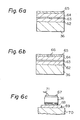
- first and second slide parts 32 and 33 are slid by a rod 60, as shown in Fig. 5c, so as to bring the solution 45 into contact with the GaAs substrate 35, whereby a first compound semiconductor layer 62 (Fig. 6a) is epitaxially formed on the substrate 35.
- the slide parts 32 and 33 are further slid to bring the solutions 46, 47, and 48 into contact with the GaAs substrate 36 in sequence, so that second, third, and fourth compound semiconductor layers 63, 64, and 65 are epitaxially formed on the substrate 36.
- Contacting times (i.e., growing times) of the solutions, compositions, thickness, and carrier concentration of the obtained layer 62 to 65 are shown in Table 2.
- the GaP plates 51 to 54 are simultaneously brought into contact with the solutions 45 to 48, so that the duration of contact may be too long for the fourth solution 40.
- the duration of contact for each of the solutions 45 to 48 can be controlled by adjusting the movement of the separator 34.
- Each of the four epitaxal layers 62 to 65 formed on the GaAs substrate 36 (Fig. 6a) is lattice-matched to the substrate 36 with a lattice constant difference of less than 0.1%. Thus, the crystals of the epitaxial layers are excellent.
- the p-type second InGaAsP layer 63 searves as an active layer, and the n-type first InGaP layer 62 and the p-type third InGaP layer 64 are clad layers.
- the n-type fourth InGaAsP layer 65 is formed for providing a stripe conducting region 66 (Fig. 6b).
- the stripe region 66 is formed by selectively doping impurities of Zn into the fourth layer 65.
- an AuSn alloy layer 67 (Fig. 6c) is formed on the GaAs substrate 36, and an AuZn alloy layer 68 is formed on the fourth epitaxal layer 65 by a vacuum evaporation method. These alloy layers 67 and 68 are heat trated to make them ohmic electrodes.
- the obtained substrate 36 is cleaved into semiconductor laser chips.
- the chip is attached on a heat sink 69 in the p-side down manner, as shown in Fig. 6c, the heat sink 69 being fixed on a stem 70.
- a wire 71 is bonded to the AuSn alloy layer (i.e., the n-electrode) 67.
- a semiconductor laser device is produced.
- the obtained laser device operates at about 25°C (room temperature)
- CW continuous wave
- the oscillating wavelength is 730 nm and the oscillating threshold current is 120 mA.
- the present invention is not restricted to the above-mentioned examples, and that many variations are possible by persons with ordinary skill in the art.
- various compound semiconductor layers of III-V and II-VI groups can be epitaxially formed in accordance with the LPE method of the present invention.
- the substrate and the crystalline plate i.e., solute source plate
- the solution and the precipitating crystal may be quaternary or a more multicomponent system.
- the solution Before the unsaturated solution is brought into contact with the solute source plate, the solution may contain all components for the epitaxial layer.
Landscapes
- Chemical & Material Sciences (AREA)
- Engineering & Computer Science (AREA)
- Crystallography & Structural Chemistry (AREA)
- Materials Engineering (AREA)
- Metallurgy (AREA)
- Organic Chemistry (AREA)
- Inorganic Chemistry (AREA)
- Liquid Deposition Of Substances Of Which Semiconductor Devices Are Composed (AREA)
- Crystals, And After-Treatments Of Crystals (AREA)
Applications Claiming Priority (2)
| Application Number | Priority Date | Filing Date | Title |
|---|---|---|---|
| JP72442/82 | 1982-04-28 | ||
| JP57072442A JPS6028799B2 (ja) | 1982-04-28 | 1982-04-28 | 液相エピタキシヤル成長方法 |
Publications (2)
| Publication Number | Publication Date |
|---|---|
| EP0093569A1 true EP0093569A1 (de) | 1983-11-09 |
| EP0093569B1 EP0093569B1 (de) | 1988-11-02 |
Family
ID=13489401
Family Applications (1)
| Application Number | Title | Priority Date | Filing Date |
|---|---|---|---|
| EP83302358A Expired EP0093569B1 (de) | 1982-04-28 | 1983-04-26 | Verfahren zur Flüssigphasenepitaxie |
Country Status (5)
| Country | Link |
|---|---|
| US (1) | US4498937A (de) |
| EP (1) | EP0093569B1 (de) |
| JP (1) | JPS6028799B2 (de) |
| CA (1) | CA1204526A (de) |
| DE (1) | DE3378374D1 (de) |
Cited By (1)
| Publication number | Priority date | Publication date | Assignee | Title |
|---|---|---|---|---|
| FR2583782A1 (fr) * | 1985-06-24 | 1986-12-26 | Slempkes Serge | Procede de depot par epitaxie en phase liquide sur un substrat, d'un alliage au moins quaternaire, et dispositif semi-conducteur comportant un tel alliage |
Families Citing this family (1)
| Publication number | Priority date | Publication date | Assignee | Title |
|---|---|---|---|---|
| US4578126A (en) * | 1983-06-22 | 1986-03-25 | Trw Inc. | Liquid phase epitaxial growth process |
Citations (1)
| Publication number | Priority date | Publication date | Assignee | Title |
|---|---|---|---|---|
| US4179317A (en) * | 1977-05-31 | 1979-12-18 | Kokusai Denshin Denwa Kabushiki Kaisha | Method for producing compound semiconductor crystals |
Family Cites Families (9)
| Publication number | Priority date | Publication date | Assignee | Title |
|---|---|---|---|---|
| BE754519A (fr) * | 1969-08-06 | 1971-02-08 | Motorola Inc | Procede et appareil pour la croissance de couches epitaxiales en phase liquide sur des semi-conducteurs |
| BE788374A (fr) * | 1971-12-08 | 1973-01-02 | Rca Corp | Procede de depot d'une couche epitaxiale d'un materiau semi-conducteur sur la surface d'un substrat |
| US3793093A (en) * | 1973-01-12 | 1974-02-19 | Handotai Kenkyu Shinkokai | Method for producing a semiconductor device having a very small deviation in lattice constant |
| US4088514A (en) * | 1975-04-17 | 1978-05-09 | Matsushita Electric Industrial Co., Ltd. | Method for epitaxial growth of thin semiconductor layer from solution |
| US4110133A (en) * | 1976-04-29 | 1978-08-29 | The Post Office | Growth of semiconductor compounds by liquid phase epitaxy |
| US4287485A (en) * | 1977-07-18 | 1981-09-01 | Massachusetts Institute Of Technology | GaInAsP/InP Double-heterostructure lasers |
| US4246050A (en) * | 1979-07-23 | 1981-01-20 | Varian Associates, Inc. | Lattice constant grading in the Aly Ca1-y As1-x Sbx alloy system |
| US4373989A (en) * | 1981-11-30 | 1983-02-15 | Beggs James M Administrator Of | Controlled in situ etch-back |
| FR2519032A1 (fr) * | 1981-12-28 | 1983-07-01 | Benchimol Jean Louis | Procede de depot par epitaxie en phase liquide d'un compose ternaire |
-
1982
- 1982-04-28 JP JP57072442A patent/JPS6028799B2/ja not_active Expired
-
1983
- 1983-04-25 CA CA000426610A patent/CA1204526A/en not_active Expired
- 1983-04-26 EP EP83302358A patent/EP0093569B1/de not_active Expired
- 1983-04-26 DE DE8383302358T patent/DE3378374D1/de not_active Expired
- 1983-04-28 US US06/489,348 patent/US4498937A/en not_active Expired - Fee Related
Patent Citations (1)
| Publication number | Priority date | Publication date | Assignee | Title |
|---|---|---|---|---|
| US4179317A (en) * | 1977-05-31 | 1979-12-18 | Kokusai Denshin Denwa Kabushiki Kaisha | Method for producing compound semiconductor crystals |
Non-Patent Citations (1)
| Title |
|---|
| JOURNAL OF CRYSTAL GROWTH, vol. 53, no. 2, May 1981, pages 413-417, North-Holland Publishing Company, Amsterdam, NL. * |
Cited By (1)
| Publication number | Priority date | Publication date | Assignee | Title |
|---|---|---|---|---|
| FR2583782A1 (fr) * | 1985-06-24 | 1986-12-26 | Slempkes Serge | Procede de depot par epitaxie en phase liquide sur un substrat, d'un alliage au moins quaternaire, et dispositif semi-conducteur comportant un tel alliage |
Also Published As
| Publication number | Publication date |
|---|---|
| CA1204526A (en) | 1986-05-13 |
| JPS6028799B2 (ja) | 1985-07-06 |
| JPS58190895A (ja) | 1983-11-07 |
| US4498937A (en) | 1985-02-12 |
| DE3378374D1 (en) | 1988-12-08 |
| EP0093569B1 (de) | 1988-11-02 |
Similar Documents
| Publication | Publication Date | Title |
|---|---|---|
| US4383872A (en) | Method of growing a doped III-V alloy layer by molecular beam epitaxy utilizing a supplemental molecular beam of lead | |
| US3960618A (en) | Epitaxial growth process for compound semiconductor crystals in liquid phase | |
| US4479222A (en) | Diffusion barrier for long wavelength laser diodes | |
| Takahei et al. | Low temperature liquid phase epitaxy growth for room‐temperature cw operation of 1.55‐μm InGaAsP/InP double‐heterostructure laser | |
| US4575742A (en) | Epitaxial wafer for use in the production of an infrared LED | |
| US4372791A (en) | Method for fabricating DH lasers | |
| US4142924A (en) | Fast-sweep growth method for growing layers using liquid phase epitaxy | |
| US4287485A (en) | GaInAsP/InP Double-heterostructure lasers | |
| EP0093569B1 (de) | Verfahren zur Flüssigphasenepitaxie | |
| US4246050A (en) | Lattice constant grading in the Aly Ca1-y As1-x Sbx alloy system | |
| US4592791A (en) | Liquid phase epitaxial growth method for producing a III-V group compound semiconductor | |
| US4464211A (en) | Method for selective area growth by liquid phase epitaxy | |
| EP0322465B1 (de) | Verfahren zum epitaktischen wachstum eines substrats für hochbrillante led | |
| Oe et al. | Liquid phase epitaxial growth of GaInP/AlGaAs double heterostructures for visible lasers | |
| US4574730A (en) | Melt dispensing liquid phase epitaxy boat | |
| US4609411A (en) | Liquid-phase epitaxial growth method of a IIIb-Vb group compound | |
| US4439399A (en) | Quaternary alloy | |
| US4179317A (en) | Method for producing compound semiconductor crystals | |
| GB2066299A (en) | Growing doped III-V alloy layers by molecular beam epitaxy | |
| Lynch et al. | GaAs/(GaAl) as laser technology | |
| Wright et al. | InGaPAs-InP double-heterojunction high-radiance LED's | |
| GB2080619A (en) | Epitaxial semiconductor device | |
| EP0330152A2 (de) | Lichtemitierendes Halbleiterbauelement | |
| Ueda | Materials Issues and Device-Degradation in the Ingaas (P)/Inp System | |
| Nagai | LPE and Characteristics of GaInAsP/InP 1.5 µm Region Laser Diodes |
Legal Events
| Date | Code | Title | Description |
|---|---|---|---|
| PUAI | Public reference made under article 153(3) epc to a published international application that has entered the european phase |
Free format text: ORIGINAL CODE: 0009012 |
|
| AK | Designated contracting states |
Designated state(s): DE FR GB NL |
|
| 17P | Request for examination filed |
Effective date: 19840419 |
|
| GRAA | (expected) grant |
Free format text: ORIGINAL CODE: 0009210 |
|
| AK | Designated contracting states |
Kind code of ref document: B1 Designated state(s): DE FR GB NL |
|
| ET | Fr: translation filed | ||
| REF | Corresponds to: |
Ref document number: 3378374 Country of ref document: DE Date of ref document: 19881208 |
|
| PLBE | No opposition filed within time limit |
Free format text: ORIGINAL CODE: 0009261 |
|
| STAA | Information on the status of an ep patent application or granted ep patent |
Free format text: STATUS: NO OPPOSITION FILED WITHIN TIME LIMIT |
|
| 26N | No opposition filed | ||
| PGFP | Annual fee paid to national office [announced via postgrant information from national office to epo] |
Ref country code: FR Payment date: 19960410 Year of fee payment: 14 |
|
| PGFP | Annual fee paid to national office [announced via postgrant information from national office to epo] |
Ref country code: GB Payment date: 19960417 Year of fee payment: 14 |
|
| PGFP | Annual fee paid to national office [announced via postgrant information from national office to epo] |
Ref country code: DE Payment date: 19960429 Year of fee payment: 14 |
|
| PGFP | Annual fee paid to national office [announced via postgrant information from national office to epo] |
Ref country code: NL Payment date: 19960430 Year of fee payment: 14 |
|
| PG25 | Lapsed in a contracting state [announced via postgrant information from national office to epo] |
Ref country code: GB Effective date: 19970426 |
|
| PG25 | Lapsed in a contracting state [announced via postgrant information from national office to epo] |
Ref country code: NL Effective date: 19971101 |
|
| GBPC | Gb: european patent ceased through non-payment of renewal fee |
Effective date: 19970426 |
|
| PG25 | Lapsed in a contracting state [announced via postgrant information from national office to epo] |
Ref country code: FR Free format text: LAPSE BECAUSE OF NON-PAYMENT OF DUE FEES Effective date: 19971231 |
|
| PG25 | Lapsed in a contracting state [announced via postgrant information from national office to epo] |
Ref country code: DE Free format text: LAPSE BECAUSE OF NON-PAYMENT OF DUE FEES Effective date: 19980101 |
|
| NLV4 | Nl: lapsed or anulled due to non-payment of the annual fee |
Effective date: 19971101 |
|
| REG | Reference to a national code |
Ref country code: FR Ref legal event code: ST |