EP0093557A2 - Schnelle integrierte komplementäre Halbleiterschaltung - Google Patents
Schnelle integrierte komplementäre Halbleiterschaltung Download PDFInfo
- Publication number
- EP0093557A2 EP0093557A2 EP83302315A EP83302315A EP0093557A2 EP 0093557 A2 EP0093557 A2 EP 0093557A2 EP 83302315 A EP83302315 A EP 83302315A EP 83302315 A EP83302315 A EP 83302315A EP 0093557 A2 EP0093557 A2 EP 0093557A2
- Authority
- EP
- European Patent Office
- Prior art keywords
- lead
- substrate
- pbte
- monocrystalline
- substrative
- Prior art date
- Legal status (The legal status is an assumption and is not a legal conclusion. Google has not performed a legal analysis and makes no representation as to the accuracy of the status listed.)
- Granted
Links
Images

Classifications
-
- H—ELECTRICITY
- H10—SEMICONDUCTOR DEVICES; ELECTRIC SOLID-STATE DEVICES NOT OTHERWISE PROVIDED FOR
- H10D—INORGANIC ELECTRIC SEMICONDUCTOR DEVICES
- H10D86/00—Integrated devices formed in or on insulating or conducting substrates, e.g. formed in silicon-on-insulator [SOI] substrates or on stainless steel or glass substrates
-
- H—ELECTRICITY
- H10—SEMICONDUCTOR DEVICES; ELECTRIC SOLID-STATE DEVICES NOT OTHERWISE PROVIDED FOR
- H10D—INORGANIC ELECTRIC SEMICONDUCTOR DEVICES
- H10D62/00—Semiconductor bodies, or regions thereof, of devices having potential barriers
- H10D62/80—Semiconductor bodies, or regions thereof, of devices having potential barriers characterised by the materials
- H10D62/874—Semiconductor bodies, or regions thereof, of devices having potential barriers characterised by the materials being Pb compounds or alloys, e.g. PbO
Definitions
- the present invention relates to a semiconductor device having a high-speed operation. More specifically, the present invention is concerned with a semiconductor integrated circuit device which operates with high-speed and which is of a complementary structure.
- the operational speed of a semiconductor integrated circuit device is limited by the carrier mobility of electrons or holes allowed to flow between the elements. Therefore, when it is desired to improve the operational speed of the device, it is necessary to increase the carrier mobility.
- the semiconductive material currently in use methods which include (1) using a compound semiconductive material such as GaAs, A1 x Ga l - x As, etc.
- the carrier mobility of a semiconductor integrated circuit device prepared by the above-mentioned methods is several thousands of square centimeters/V.sec to several tens of thousands of square centimeters/V.sec at best.
- the manufacturing yield of the semiconductor device decreases due to the technical problem involved in the manufacturing steps.
- the semiconductor device of a complementary circuit structure has excellent characteristics such as a high degree of permissible noise, a low power consumption, etc. and is therefore regarded as being a promising device providing excellent cost performance.
- the operational speed of the complementary semiconductor integrated circuit device is limited by the smaller one of its electron or hole mobility.
- the hole mobility at room temperature of the said compound semiconductive material is only several hundreds of square centimeters/V.sec at most, with the result that the final operational speed of the complementary semiconductor device is not improved because, even when the mobility of one carrier (electron) of the complementary semiconductor device is increased, the final operational speed is limited by this inferior- hole mobility if the mobility of the other carrier (hole) is relatively small. Accordingly, the increase in speed of the complementary semiconductor integrated circuit does not reach the desired speed even if concurrent use is made of a technique for lowering the atmospheric temperature.
- the object of the present invention is to provide a new and improved semiconductor device which has excellent hole and electron carrier mobilities and which has high-speed operation even when it is applied to a complementary circuit structure.
- the active elements such as FETs or bipolar transistors are preferably formed of lead chalcogenide based semiconductive material such as PbS, PbSe, or PbTe.
- This type of semiconductive material is higher both in electron mobility and in hole mobility than silicon and the values of its electron and hole mobilities are approximate to each other.
- the lead chalcogenide semiconductive material has, in a temperature zone of, for example, liquid helium, electron and hole carrier mobilities of several tens of thousands of square centimeters to several hundreds of thousands of square centimeters/V ⁇ sec.
- a semiconductor integrated circuit device which has higher speed than that of the conventional semiconductor integrated circuit device to the extent corresponding to an increase, by at least one digit-place, of the operational speed value of that conventional one.
- the above-mentioned active elements constituting the complementary semiconductor integrated circuit, of the present invention are, as mentioned above, constituted by FETs or bipolar transistors.
- a pair of transistors which perform a logical switching operation on a mutually complementary basis, one of such transistors operates with the holes as its "active carrier” and the other thereof operates with the electron as its "active carrier".
- active carrier used in this specification and claims is defined to mean “carrier directly serving to perform the active function of the transistor”.
- FET or unipolar transistor operating with the holes as "active carrier” it means a p-channel FET whose channel region is formed by the holes.
- a bipolar transistor operating with the holes as "active carrier” such transistor means a pnp type transistor. The same applies to the case of "electron”.
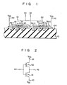
- a monocrystalline substrate 10 consisting of an electrically insulative substrate such as BaF 2 has a cleavage plane 10a corresponding to a specified crystalline face on its upper surface.
- an n-conductivity type thin monocrystalline film A l and a p-conductivity type monocrystalline thin film A 2 are each deposited by being selectively epitaxially grown thereon through the use of, a molecular beam epitaxy technique, for example.
- These films A l and A 2 are each formed of a semiconductor crystalline body which has higher carrier mobility or electron and hole mobilities than silicon and the electron and hole mobilities are approximate to each other.
- This semiconductor crystalline body is preferably formed of lead chalcogenide.
- PbTe is utilized as the lead chalcogenide constituting the films A 1 and A 2 .
- P-conductivity type impurities are introduced into the PbTe monocrystalline film A l except a middle film region 12, corresponding to a channel region, by a known selective diffusion or ion-implantation technique, whereby two outer film regions 16 and 18 of the film A l has a p +- conductivity type.
- the two outer film regions 16 and 18 correspond to source and drain, respectively.
- a p-channel FET Q 1 is formed on the insulative substrate 10 to have the PbTe monocrystalline channel region 12 of n-conductivity type and the PbTe monocrystalline source and drain films 16 and 18 of p +- conductivity type.
- n-conductivity type impurities are introduced into the other PbTe monocrystalline film A 2 except a channel region 14 so as to cause two outer film regions serving as source and drain regions 20 and 22 to have an n +- conductivity.
- Gate insulation films 24 and 26 are each formed on the films A l and A 2 each having a pnp junction structure and npn junction structure.
- gate insulation films 24 and 26, are each formed of a thin film having a high dielectric constant such as that made of Si 3 N 4 , Ta 2 0 5 and the like. Gate electrodes 32 and 34 are further deposited on these films 24 and 26, respectively. Thus, the p-channel metal-insulator semiconductor (MIS) FET Q 1 and the n-channel MISFET Q 2 are finally formed on the insulative substrate 10. Thereafter, wiring patterns 36-l, 36-2 and 36-3 consisting of metallic material such as platinum are formed on the above structure by a known technique.
- MIS metal-insulator semiconductor
- the patterns 36-1 and 36-2 are in contact with the PbTe films 16 and 22, thereby providing a source electrode (36-1) for the MISFET Q 1 and a drain electrode (36-2) for the MISFET Q 2 , respectively.
- the PbTe films 18 and 20 are electrically connected to each other by means of the platinum layer 36-3.
- the source electrode 36-1 of the MISFET Q 1 is connected to a power source terminal 40 to which a grounding potential or a potential V SS is applied, while the drain electrode 36-2 of the MISFET Q 2 is connected to another power source terminal 42 to which a voltage V DD is applied.
- the gate electrodes 32 and 34 of the MISFETs Q l and Q 2 are commonly connected, and at the same time, connected to a signal input terminal 44.
- Fig. 2 shows an equivalent circuit of the integrated circuit of Fig. 1.
- the complementary inverter circuit including MISFETs Q l and Q 2 and having the foregoing construction of one embodiment of the invention exhibits an excellent high-speed characteristic as compared with a conventional integrated CMOS inverter circuit.
- the monocrystalline thin films consisting of lead chalcogenide such as PbTe and formed by selective molecular beam epitaxy which have an electron carrier mobility of approximately 1700 cm 2 /V.sec and a hole carrier mobility of approximately 900 cm 2 /V.sec at room temperature have, in the zone of liquid helium temperature, an electron carrier mobility as high as 5 x 10 5 cm 2 /V.sec and a hole carrier mobility as high as approximately 3 x 10 5 cm 2 /V.sec.
- lead chalcogenide such as PbTe and formed by selective molecular beam epitaxy
- the lead chalcogenide based semiconductor materials generally have a high specific dielectric constant of several hundred.
- PbTe one of the lead chalcogenide compounds, also has a specific dielectric constant as high as approximately 400.
- An increase in capacitance of the electrode section, which is attributable to such a high dielectric constant may therefore occur.
- the monocrystalline thin film made of PbTe and constituting an active layer was formed on the insulative substrate 10 and therefore the increase in capacitance of the electrode section can be largely suppressed.
- the above-mentioned layer structure according to the invention makes it easy to manufacture a ballistic device because the mean free path of the electron and hole carriers of lead chalcogenide in the temperature zone of liquid helium is as large as scores of microns.
- the fact that the mean free path of the carriers is long makes it possible to enlarge the scale of an active region of the ballistic device.
- the existing integrated element fabrication technique is therefore sufficient for manufacturing the ballistic device.
- the monocrystalline thin film such as that made of BaF 2 , SrF 2 and the like is formed as the gate insulative layer on the lead chalcogenide made film, it is possible to further improve the operational characteristics of MISFET because the interface property of MISFET is improved.
- Figs. 3 and 4 there are shown modifications of the complementary integrated inverter circuit shown in Fig. 1, respectively.
- the MISFETs Q 1 and Q 2 are provided on a substrative body 50 comprised of an electrical conductive substrate 52 and an electrical insulative thin film 54 formed on the surface 52a of that substrate 52.
- the substrate 52 is composed of a monocrystalline bulk of PbTe or one of the lead chalcogenide compounds which is the same material as that used for the FETs Q l and Q 2 .
- the insulative thin film 54 consists of a monocrystalline material which is lattice-matched with the lead chalcogenide based semiconductive material, for example, BaF 2 .
- the lead chalcogenide based semiconductive material for example, BaF 2 .
- the MISFETs Q 1 and Q 2 are formed directly on the cleavage plane 10a of the BaF 2 substrate 10 and therefore the PbTe thin film structures A l and A 2 constituting the FETs Q 1 and Q 2 are very likely to have imperfections and lattice defects due to stress on the cleavage plane 10a. As a result, the operation speed of the MISFETs Q l and Q 2 decreases.
- the irregularities in crystalline structure of the surface 52a of the PbTe substrate 52 are removed in the growth process of the BaF 2 insulative thin film 54 on the PbTe substrate 52. This reliably prevents lattice defects from being produced in the PbTe thin film structures A l and A 2 .
- Figs. 1 and 3 there has been shown the complementary integrated inverter circuit comprised of MISFETs Q 1 and Q 2 .
- the transistor elements constituting the logic circuit are not limited to MISFETs but may be junction-gate field effect transistors (abbreviated as J-FET).
- Fig. 4 there is shown one example of the complementary inverter circuit constructed of a pair of J-FETs Q 3 and Q 4 .
- the J-FET 0 3 at one side is constructed such that p +- type monocrystalline PbTe thin films 60 and 62 are formed on the substrate 10 and a p-type PbTe thin film 64 corresponding to a channel constituting a current path is formed between the films 60 and 62 so as to be joined to the films 60 and 62 from both sides thereof.
- An n +- type PbTe thin film 66 and a gate electrode 32 are deposited on the intermediate PbTe thin film 64 in the order mentioned.
- the J-FET Q 4 at the other side also includes n +- type monocrystalline PbTe thin films 68 and 70, an n-type PbTe thin film 72 formed between the films 68 and 70 so as to constitute the channel, and a p +- type PbTe film 74 formed on the film 72.
- the notation D 2 denotes a depletion region formed in the channel 72.
- the complementary inverter circuit of Fig. 4 it is unnecessary to provide the gate insulation films 24 and 26 of the MISFETs Q l and Q 2 constituting the inverter circuit of Fig. 1.
- controlling the thickness of the gate insulation film with high precision is required to precisely set the threshold level involved in the switching operation of FET.
- This control of film thickness is one of the factors which makes it difficult to manufacture the complementary integrated inverter circuit device.
- Fig. 4 since the J-FET structure has been adopted, it is not necessary to provide the gate insulation film as mentioned above. This means that the parameters for controlling the threshold level are reduced by one.
- the present invention can also be effectively applied to a complementary integrated logic circuit comprised of active elements other than the transistors employed in the above-mentioned embodiments, for example, Schottky gate transistors.
- a complementary integrated logic circuit comprised of active elements other than the transistors employed in the above-mentioned embodiments, for example, Schottky gate transistors.
- PbS or PbSe as the lead chalcogenide provides the same effect as that attainable by the preceding embodiments since the electron and hole mobilities are high in the temperature zone of liquid helium.
- the present invention can also be applied to what is called "a three-dimensional semiconductor integrated circuit device" constructed by using the monocrystalline thin film such as that made of the BaF 2 , SrF 2 or the like as interlayer insulative films and stacking the lead chalcogenide monocrystalline thin films.
- the lead chalcogenide monocrystalline thin film serving as an active element is grown on the electrical insulative substrate such as that made of BaF 2 to reduce the electrode capacitance.
- the substrate be electrically insulative to achieve the effect of the present invention. Because the electrode capacitance can be reduced by minituarizing the area of electrode it can be expected that the active layer consisting of the lead chalcogenide thin film is formed on the monocrystalline bulk of lead chalcogenide.
- Table 2 presented below shows the electron and hole mobilities of each of PbS, PbSe and PbTe in a temperature zone of liquid nitrogen.
Landscapes
- Metal-Oxide And Bipolar Metal-Oxide Semiconductor Integrated Circuits (AREA)
- Bipolar Integrated Circuits (AREA)
Applications Claiming Priority (2)
| Application Number | Priority Date | Filing Date | Title |
|---|---|---|---|
| JP57068844A JPS58186961A (ja) | 1982-04-26 | 1982-04-26 | 半導体装置 |
| JP68844/82 | 1982-04-26 |
Publications (3)
| Publication Number | Publication Date |
|---|---|
| EP0093557A2 true EP0093557A2 (de) | 1983-11-09 |
| EP0093557A3 EP0093557A3 (en) | 1985-09-11 |
| EP0093557B1 EP0093557B1 (de) | 1989-07-12 |
Family
ID=13385397
Family Applications (1)
| Application Number | Title | Priority Date | Filing Date |
|---|---|---|---|
| EP83302315A Expired EP0093557B1 (de) | 1982-04-26 | 1983-04-22 | Schnelle integrierte komplementäre Halbleiterschaltung |
Country Status (3)
| Country | Link |
|---|---|
| EP (1) | EP0093557B1 (de) |
| JP (1) | JPS58186961A (de) |
| DE (1) | DE3380195D1 (de) |
Cited By (3)
| Publication number | Priority date | Publication date | Assignee | Title |
|---|---|---|---|---|
| US4847666A (en) * | 1987-12-17 | 1989-07-11 | General Motors Corporation | Hot electron transistors |
| FR2666175A1 (fr) * | 1990-08-21 | 1992-02-28 | Thomson Csf | Transistor a effet de champ a supraconducteur. |
| EP2068368A3 (de) * | 2007-12-06 | 2009-08-05 | Electronics and Telecommunications Research Institute | Verfahren zur Herstellung von n-leitendem und p-leitendem Chalcogenid-Material, dotierter Chalcogenid-Homoübergangsdünnschichttransistor und Verfahren zu dessen Herstellung |
Families Citing this family (1)
| Publication number | Priority date | Publication date | Assignee | Title |
|---|---|---|---|---|
| JPS6394168U (de) * | 1986-12-11 | 1988-06-17 |
Family Cites Families (6)
| Publication number | Priority date | Publication date | Assignee | Title |
|---|---|---|---|---|
| US3405331A (en) * | 1966-06-29 | 1968-10-08 | Navy Usa | Insulated gate field effect transistor using lead salt |
| DE2103573A1 (de) * | 1971-01-26 | 1972-08-03 | Siemens Ag | Integriertes Halbleiterbauelement, insbesondere verlustarmes Speicherelement, in Komplementärkanal-Technik |
| US3958266A (en) * | 1974-04-19 | 1976-05-18 | Rca Corporation | Deep depletion insulated gate field effect transistors |
| US4171996A (en) * | 1975-08-12 | 1979-10-23 | Gosudarstvenny Nauchno-Issledovatelsky i Proektny Institut Redkonetallicheskoi Promyshlennosti "Giredmet" | Fabrication of a heterogeneous semiconductor structure with composition gradient utilizing a gas phase transfer process |
| CA1063254A (en) * | 1975-09-04 | 1979-09-25 | Shu-Yau Wu | Electrostatically bonded semiconductor-on-insulator mos device, and a method of making the same |
| US4126732A (en) * | 1977-08-16 | 1978-11-21 | The United States Of America As Represented By The Secretary Of The Navy | Surface passivation of IV-VI semiconductors with As2 S3 |
-
1982
- 1982-04-26 JP JP57068844A patent/JPS58186961A/ja active Granted
-
1983
- 1983-04-22 EP EP83302315A patent/EP0093557B1/de not_active Expired
- 1983-04-22 DE DE8383302315T patent/DE3380195D1/de not_active Expired
Cited By (6)
| Publication number | Priority date | Publication date | Assignee | Title |
|---|---|---|---|---|
| US4847666A (en) * | 1987-12-17 | 1989-07-11 | General Motors Corporation | Hot electron transistors |
| FR2666175A1 (fr) * | 1990-08-21 | 1992-02-28 | Thomson Csf | Transistor a effet de champ a supraconducteur. |
| EP0478399A1 (de) * | 1990-08-21 | 1992-04-01 | Thomson-Csf | Supraleitender Feldeffekttransistor |
| US5231295A (en) * | 1990-08-21 | 1993-07-27 | Thomson-Csf | Superconducting field effect transistor |
| EP2068368A3 (de) * | 2007-12-06 | 2009-08-05 | Electronics and Telecommunications Research Institute | Verfahren zur Herstellung von n-leitendem und p-leitendem Chalcogenid-Material, dotierter Chalcogenid-Homoübergangsdünnschichttransistor und Verfahren zu dessen Herstellung |
| US8039926B2 (en) | 2007-12-06 | 2011-10-18 | Electronics And Telecommunications Research Institute | Method for manufacturing N-type and P-type chalcogenide material, doped homojunction chalcogenide thin film transistor and method of fabricating the same |
Also Published As
| Publication number | Publication date |
|---|---|
| JPS6238864B2 (de) | 1987-08-20 |
| JPS58186961A (ja) | 1983-11-01 |
| EP0093557B1 (de) | 1989-07-12 |
| DE3380195D1 (en) | 1989-08-17 |
| EP0093557A3 (en) | 1985-09-11 |
Similar Documents
| Publication | Publication Date | Title |
|---|---|---|
| US5155571A (en) | Complementary field effect transistors having strained superlattice structure | |
| US4568958A (en) | Inversion-mode insulated-gate gallium arsenide field-effect transistors | |
| EP0323896B1 (de) | Komplementäre Halbleiteranordnung | |
| JP3135939B2 (ja) | Hemt型半導体装置 | |
| KR970004457B1 (ko) | 반도체 장치 및 그 제조 방법 | |
| US5986287A (en) | Semiconductor structure for a transistor | |
| US5416354A (en) | Inverted epitaxial process semiconductor devices | |
| EP0144242A2 (de) | Integrierte Halbleiterschaltungsanordnung mit Verbindungsmaterial | |
| KR950006477B1 (ko) | 반도체장치 및 그 제조방법 | |
| JPH0371776B2 (de) | ||
| JPH027532A (ja) | 積層チャネル電界効果トランジスタ | |
| US7164160B2 (en) | Integrated circuit device with a vertical JFET | |
| US5041892A (en) | Homo-junction bipolar transistor having high base concentration and suitable for low temperature operation | |
| US3639813A (en) | Complementary enhancement and depletion mosfets with common gate and channel region, the depletion mosfet also being a jfet | |
| US3804681A (en) | Method for making a schottky-barrier field effect transistor | |
| EP0093557A2 (de) | Schnelle integrierte komplementäre Halbleiterschaltung | |
| US4117587A (en) | Negative-resistance semiconductor device | |
| JPS61147577A (ja) | 相補型半導体装置 | |
| US5107314A (en) | Gallium antimonide field-effect transistor | |
| US4965645A (en) | Saturable charge FET | |
| JP2611358B2 (ja) | 半導体装置 | |
| JPH0384960A (ja) | 半導体装置 | |
| KR910006751B1 (ko) | 반도체 집적회로장치 및 그의 제조방법 | |
| JP2655594B2 (ja) | 集積型半導体装置 | |
| Warabisako et al. | Characterization of laser-SOI double Si active layers by fabricating elementary device structures |
Legal Events
| Date | Code | Title | Description |
|---|---|---|---|
| PUAI | Public reference made under article 153(3) epc to a published international application that has entered the european phase |
Free format text: ORIGINAL CODE: 0009012 |
|
| 17P | Request for examination filed |
Effective date: 19830503 |
|
| AK | Designated contracting states |
Designated state(s): DE FR GB IT NL |
|
| RAP1 | Party data changed (applicant data changed or rights of an application transferred) |
Owner name: KABUSHIKI KAISHA TOSHIBA |
|
| PUAL | Search report despatched |
Free format text: ORIGINAL CODE: 0009013 |
|
| AK | Designated contracting states |
Designated state(s): DE FR GB IT NL |
|
| 17Q | First examination report despatched |
Effective date: 19870602 |
|
| GRAA | (expected) grant |
Free format text: ORIGINAL CODE: 0009210 |
|
| AK | Designated contracting states |
Kind code of ref document: B1 Designated state(s): DE FR GB NL |
|
| REF | Corresponds to: |
Ref document number: 3380195 Country of ref document: DE Date of ref document: 19890817 |
|
| ET | Fr: translation filed | ||
| PLBE | No opposition filed within time limit |
Free format text: ORIGINAL CODE: 0009261 |
|
| STAA | Information on the status of an ep patent application or granted ep patent |
Free format text: STATUS: NO OPPOSITION FILED WITHIN TIME LIMIT |
|
| 26N | No opposition filed | ||
| PGFP | Annual fee paid to national office [announced via postgrant information from national office to epo] |
Ref country code: FR Payment date: 19930408 Year of fee payment: 11 |
|
| PGFP | Annual fee paid to national office [announced via postgrant information from national office to epo] |
Ref country code: GB Payment date: 19930414 Year of fee payment: 11 |
|
| PGFP | Annual fee paid to national office [announced via postgrant information from national office to epo] |
Ref country code: NL Payment date: 19930430 Year of fee payment: 11 |
|
| PGFP | Annual fee paid to national office [announced via postgrant information from national office to epo] |
Ref country code: DE Payment date: 19930506 Year of fee payment: 11 |
|
| PG25 | Lapsed in a contracting state [announced via postgrant information from national office to epo] |
Ref country code: GB Effective date: 19940422 |
|
| PG25 | Lapsed in a contracting state [announced via postgrant information from national office to epo] |
Ref country code: NL Effective date: 19941101 |
|
| NLV4 | Nl: lapsed or anulled due to non-payment of the annual fee | ||
| GBPC | Gb: european patent ceased through non-payment of renewal fee |
Effective date: 19940422 |
|
| PG25 | Lapsed in a contracting state [announced via postgrant information from national office to epo] |
Ref country code: FR Effective date: 19941229 |
|
| PG25 | Lapsed in a contracting state [announced via postgrant information from national office to epo] |
Ref country code: DE Effective date: 19950103 |
|
| REG | Reference to a national code |
Ref country code: FR Ref legal event code: ST |