EP0093450A2 - Differential pressure apparatus - Google Patents
Differential pressure apparatus Download PDFInfo
- Publication number
- EP0093450A2 EP0093450A2 EP83104327A EP83104327A EP0093450A2 EP 0093450 A2 EP0093450 A2 EP 0093450A2 EP 83104327 A EP83104327 A EP 83104327A EP 83104327 A EP83104327 A EP 83104327A EP 0093450 A2 EP0093450 A2 EP 0093450A2
- Authority
- EP
- European Patent Office
- Prior art keywords
- junction
- resistor
- junctions
- bridge
- amplifier
- Prior art date
- Legal status (The legal status is an assumption and is not a legal conclusion. Google has not performed a legal analysis and makes no representation as to the accuracy of the status listed.)
- Withdrawn
Links
Images


Classifications
-
- G—PHYSICS
- G01—MEASURING; TESTING
- G01L—MEASURING FORCE, STRESS, TORQUE, WORK, MECHANICAL POWER, MECHANICAL EFFICIENCY, OR FLUID PRESSURE
- G01L1/00—Measuring force or stress, in general
- G01L1/20—Measuring force or stress, in general by measuring variations in ohmic resistance of solid materials or of electrically-conductive fluids; by making use of electrokinetic cells, i.e. liquid-containing cells wherein an electrical potential is produced or varied upon the application of stress
- G01L1/22—Measuring force or stress, in general by measuring variations in ohmic resistance of solid materials or of electrically-conductive fluids; by making use of electrokinetic cells, i.e. liquid-containing cells wherein an electrical potential is produced or varied upon the application of stress using resistance strain gauges
- G01L1/2268—Arrangements for correcting or for compensating unwanted effects
- G01L1/2281—Arrangements for correcting or for compensating unwanted effects for temperature variations
-
- G—PHYSICS
- G01—MEASURING; TESTING
- G01L—MEASURING FORCE, STRESS, TORQUE, WORK, MECHANICAL POWER, MECHANICAL EFFICIENCY, OR FLUID PRESSURE
- G01L9/00—Measuring steady of quasi-steady pressure of fluid or fluent solid material by electric or magnetic pressure-sensitive elements; Transmitting or indicating the displacement of mechanical pressure-sensitive elements, used to measure the steady or quasi-steady pressure of a fluid or fluent solid material, by electric or magnetic means
- G01L9/02—Measuring steady of quasi-steady pressure of fluid or fluent solid material by electric or magnetic pressure-sensitive elements; Transmitting or indicating the displacement of mechanical pressure-sensitive elements, used to measure the steady or quasi-steady pressure of a fluid or fluent solid material, by electric or magnetic means by making use of variations in ohmic resistance, e.g. of potentiometers, electric circuits therefor, e.g. bridges, amplifiers or signal conditioning
- G01L9/04—Measuring steady of quasi-steady pressure of fluid or fluent solid material by electric or magnetic pressure-sensitive elements; Transmitting or indicating the displacement of mechanical pressure-sensitive elements, used to measure the steady or quasi-steady pressure of a fluid or fluent solid material, by electric or magnetic means by making use of variations in ohmic resistance, e.g. of potentiometers, electric circuits therefor, e.g. bridges, amplifiers or signal conditioning of resistance-strain gauges
- G01L9/045—Measuring steady of quasi-steady pressure of fluid or fluent solid material by electric or magnetic pressure-sensitive elements; Transmitting or indicating the displacement of mechanical pressure-sensitive elements, used to measure the steady or quasi-steady pressure of a fluid or fluent solid material, by electric or magnetic means by making use of variations in ohmic resistance, e.g. of potentiometers, electric circuits therefor, e.g. bridges, amplifiers or signal conditioning of resistance-strain gauges with electric temperature compensating means
Definitions
- the invention relates to a differential pressure apparatus according to the preamble of claim 1.
- Such differential pressure apparatus is known from DE-A1-28 41 491.
- this reference has a temperate dependent resistor connected to the noninverting input of the first differential amplifier.
- a voltage regulator 10 is connected to a bridge circuit 11 by a Lead 12 that carries a voltage E c .
- Voltage E is essentially a constant regulated voLtage.
- c Bridge circuit 11 has output Leads 13 and 14 which are connected respectively to the top and bottom of a Wheatstone bridge 15.
- the output of bridge 15 is impressed upon an amplifier circuit 16 over Leads 17 and 18.
- the output of amplifier circuit 16 is impressed upon an output circuit 19 over Leads 20 and 21.
- Output circuit 19 provides a feedback signal over a Lead 22 labeled E d to bridge circuit 11.
- Output circuit 19 provides an unreguLated DC voltage E a to voltage regulator 10 over a lead 24.
- Output circuit 19 also is provided with a regulated DC voltage E b from voltage regulator 10.
- VoLtage regulator 10 also provides the same regulated voltage E b to bridge circuit 11.
- voLtage regulator 10 in Fig. 2 will be described in detail as follows.
- Regulator 10 is grounded at 23 as shown in Fig. 2.
- ReguLator 10 has output Leads 24, 25 and 12.
- ReguLator 10 has junctions at 26, 27, 28, 29, 30, 31, 32, 33, 34, 35, 36, 37, 38, 39, 40, 41, 42, 43, 44 and 45.
- Transistors 46 and 47 are provided. Both of these transistors are PNP type transistors.
- Transistor 46 has an emitter 48 connected from junction 26, a base 49 connected from junction 28, and a collector 50 connected from junction 29. Junctions 28 and 29 are connected together.
- Transistor 47 has an emitter 51 connected from junction 26, a collector 52 connected from junction 31, and a base 53 connected to junction 28.
- Another transistor 54 is also provided.
- Transistor 54 is a PNP type transistor having an emitter 55 connected from junction 29, a collector 56 connected from junction 32 and a base 57 connected from junction 31.
- Still another transistor 58 is provided having an emitter of 59 connected to a collector 62 of a twin transistor 63.
- Transistor 58 also has a collector 60 connected from junction 31, and a base 61 connected from junction 34.
- a field effect transistor (FET) 64 is also provided having a source 65 connected at junction 34 and a drain 66 connected at junction 30. Junctions 27 and 30 are connected together.
- a resistor 67 is connected between junctions 30 and 33.
- FET 64 also has a gate 68 connected to junction 33. Junctions 32 and 33 are connected together. Junctions 34, 37 and 38 all are connected together. A resistor 69 is connected between junction 35 and junction 37. A capacitor 70 is connected between junctions 35 and 36. A resistor 71 is connected between junctions 38 and 39. A resistor 72 is connected between junctions 38 and 42. A resistor 73 is connected from junction 42 to lead 12. Junctions 41 and 42 are connected together. Junctions 35 and 40 are connected together. A resistor 74 is connected between junctions 40 and 44. A resistor 75 is connected between junctions 43 and 44.
- Transistor twin 63 has one base 76 connected from junction 40.
- the second base 77 connected from junction 41, emitters 78 and 79 connected together at junction 43, and a collector 80 connected from junction 36.
- Junctions 32 and 36 are connected together.
- Transistors 58 and 63 are NPN type transistors. Zener diode 81 is connected between junctions 41 and 45. A zener diode 82 is connected between junctions 39 and 45. Lead 24 is connected from junction 27, lead 25 is connected from junction 39 and Lead 12 is connected from resistor 73. Lead 12 carries over into Fig. 3, and is connected to a junction 83. Fig. 3 has junctions 84, 85, 86, 87, 88 and 90. An operational amplifier is provided at 91 having a connection from Lead 12 via junction 83 and jumper 92 to the non-inverting input of amplifier 91.
- AmpLifier 91 has an input from junction 87 to the inverting input thereof.
- the bottom junction 120 of bridge 15 is connected to junction 87.
- the top junction 119 of bridge 15 is connected from the output Lead 93 of amplifier 91.
- Bridge 15 has output Leads 17 and 18 connected to amplifier circuit 16 as before.
- Resistors 95, 96 and 97 with the jumper 98 connects junction 83 to junction 86.
- a resistor 99 connects junction 86 to junction 88.
- Junction 88 is grounded.
- a resistor 100 is connected with a jumper 101 between junction 87 to junction 88.
- Bridge circuit 11 shown in Fig. 3 has output Leads 102, 103 and 104. Resistors 105 and 106 connect junction 86 to output Lead 102.
- AmpLifier 91 is a differential amplifier.
- an amplifier 110 is shown in Fig. 3 which is also a differential amplifier.
- AmpLifier 110 has an inverting input connected from junction 84.
- a potentiometer is provided at 107 having a winding 108 and a wiper 109.
- a resistor 111 is connected between wiper 109 and junction 84. Winding 108 is connected between Lead 103 and ground.
- An adjustable feedback resistor 112 is connected between junctions 84 and 85.
- a resistor 113 is connected from junction 19 to the noninverting input of amplifier 110.
- a resistor 113' and a potentiometer 114 are connected together at junction 90. Resistor 113' is connected between junctions 89 and 90.
- TerminaLs are provided at 115, 116 and 117. Terminal 117 is grounded. Terminal 115 is connected to output Lead 104.
- a variable resistor 118 is connected from junction 85 to terminal 116.
- Bridge 15 shown in Fig. 4 is a Wheatstone bridge. Leads 13 and 14 are connected respectively to junctions 119 and 120. Junctions 119 and 120 form upper and Lower corners of the bridge.
- a potentiometer 121 is provided having a winding 122 and a wiper 123. Winding 122 is connected between junctions 124 and 125.
- a resistor 126 is also connected between junctions 124 and 125. Terminals are provided at 127, 128, 129 and 130. Terminal 127 is connected to junction 119.
- Terminal 128 is connected to junction 124 via resistors 131 and 132.
- Terminal 129 is connected to junction 125 via resistors 133 and 134.
- Terminal 130 is connected to junction 120.
- Junctions 135 and 136 are connected together.
- a resistor 137 is connected between junctions 119 and 135.
- a resistor 138 is connected between junctions 120 and 135.
- TerminaLs are provided at 139, 140, 141, 142, 143 and 144.
- a resistor 145 is connected from potentiometer wiper 123 to terminal 143.
- TerminaLs 139 and 143 are connected together.
- a jumper 146 is provided to connect terminals 140 and 141.
- a jumper 147 is provided to connect terminals 143 and 144.
- Output leads 17 and 18 are connected respectively from terminals 141 and 144.
- Terminal 142 is connected from junction 136.
- TerminaL 140 is also connected from terminal 136.
- a strain gage 148 is connected between terminals 127 and 128.
- a second strain gage 149 is connected between terminals 129 and 130. Strain gages 148 and 149 may be physically mounted the same as or similar to those disclosed in R. E. TaLmo et aL., U.S. Patent No. 3,722,264 issued March 27, 1973.
- a differential pressure unit (DPU) 150 increases and decreases the respective resistances of strain gages 148 and 149, or vice versa. See E. A. Romo U.S. Patent No. 4,202,218 issued May 13, 1980. See also all of the references cited in the said Romo patent.
- AmpLifier circuit 16 is shown in Fig. 5 including junctions 151, 152, 153, 154, 155, 156, 157, 158, 159, 160, 166, 167, 168, 169 and 170.
- Amplifier circuit 16 is provided with a switch 165 which is a single pole triple throw switch with a pole terminal 164 and contact terminals 161, 162 and 163. PoLe terminal 164 is connected to junction 166. Junctions 166, 167 and 169 are connected together. A capacitor 171 is connected between junctions 151 and 152. Leads 17 and 18 which are the output Leads of bridge 15 shown in Fig. 4 are connected respectively to junctions 151 and 152.
- Differential amplifiers 172 and 173 are provided.
- AmpLifier 172 has an non-inverting input connected from junction 151.
- Amplifier 173 has a non-inverting input connected from junction 152.
- AmpLifier 172 has an inverting input connected from junction 154.
- Amplifier 173 has an inverting input connected from junction 166.
- the output of amplifier 172 is connected to junction 153. Junctions 153 and 155 are connected together. A resistor 174 is connected to an output Lead 175 from junction 155. A capacitor 176 is connected between junctions 153 and 154. A resistor 177 is connected between junctions 155 and 157. A potentiometer 178 is provided having a winding 179 and a wiper 180. Wiper 180 is connected from junction 157. Winding 179 and a resistor 181 are connected from junction 157 to junction 158. A resistor 182 is connected from junction 158 to junction 159. A resistor 183 is connected between junctions 159 and 160. Junctions 160 and 169 are connected together. A resistor 184 is connected between junctions 169 and 170. A capacitor 185 is connected between junctions 167 and 168.
- junction 168 The output of amplifier 173 is connected to junction 168. Junctions 168 and 170 are connected together. A resistor 186 is connected from junction 170 to an output Lead 187.
- Output circuit 19 shown in Fig. 6 includes junctions 188, 189, 190, 191, 192, 193, 194, 195, 196, 197 and 198.
- Output Leads 175 and 187 from amplifier circuit 16 shown in Fig. 5 are connected respectively to junctions 188 and 190.
- a differential amplifier is provided at 199.
- AmpLifier 199 has non-inverting input connected from junction 190 and an inverting input connected from junction 189.
- a resistor 200 is connected from the output of amplifier 199 to junction 193.
- a resistor 201 is connected between junctions 188 and 191.
- a capacitor 202 is connected between junctions 189 and 192.
- Junctions 188 and 189 are connected together.
- Junctions 191 and 192 are connected together.
- Junctions 192 and 195 are connected together.
- Lead 22 is connected to junction 191.
- a resistor 203 connects junction 193 with lead 25.
- a field effect transistor (FET) 204 is provided having a source 205, a drain 206 and a gate 207.
- Gate 207 is connected from function 193.
- Source 205 is connected from junction 195.
- Drain 206 is connected from junction 194.
- a resistor 208 is connected between junctions 195 and 196. SubstantiaLLy everything to the right of junction 196 as viewed in Fig. 6 may be remote, if desired. It is the current flow from junction 197 to junction 198 via resistor 209 that is directly proportional to the output of bridge 15 shown in Fig. 4.
- a voltmeter 210 is provided which is connected from junction 197 to junction 198 in parallel with resistor 209. If desired, voltmeter 210 may be caLibrated in pressure or differential pressure.
- a resistor 211 is connected between junctions 190 and 196. Junction 196 is grounded. From junction 198 to junction 194 through a source of potential 212, a diode 213 is connected in series. Lead 24 is connected from junction 194.
- voltage regulator 10 supplies two regulated voltages which may be utilized to control the "current" and “voLtage” amplifiers 91 and 110, respectively, shown in Fig. 3.
- Bridge circuit 11 contains feedback for causing the voltage across bridge 15 to vary with temperature the same as the remainder of the circuit does. That is, the said constant voltage is constant to within 100 divided by the gain of the bridge circuit 11 in percent.
- the gain of bridge circuit 11 may be 40 or 50, for example.
- bridge 15 The output of bridge 15 is amplified in circuit 16 and circuit 19, circuit 19 containing an indicator (voLtmeter 210) of the differential pressure measured by bridge 15.
- bridge 15 may be conventional and the strain gages 148 and 149 thereof may be conventional. Strain gages 148 and 149 may be affixed to a strain gage beam that is in turn moved according to the difference between two pressures.
- the construction of strain gages 148 and 149, their method of mounting and the construction of a differential pressure unit and a strain gage beam are all old in the art, per se. For example, see the said TaLmo and Romo patents.
- Lead 24 simply supplies the unregulated voltage E of source 212 (Fig. 6) to voltage regulator 10. See all of Figs. 1, 2 and 6.
- a regulated voltage is supplied from zener 82 as E b in Figs. 3 and 6.
- E d is directly proportional to the current through resistor 208 (Fig. 6). E d is therefore a feedback voltage for linearity as is conventional.
- the present invention shown in Fig. 1 may be entirely conventional except for bridge circuit 11 shown in Fig. 3. This circuit keeps the bridge current constant. This prevents changes in temperature from making the reading of voltmeter 210 in Fig. 6 incorrect. See the algebraic proof in the said Romo patent.
- E c is a regulated voltage from zener 81 through resistor 73 over Lead 12 from Fig. 2.
- feedback (E d ) comes over lead 102, resistors 106 and 105, jumper 98 through resistors 97, 96 and 95 via jumper 92 to the noninverting input of amplifier 91. It is applied thereto with (+) the voltage of zener 81 via resistor 73.
- a second feedback for bridge voltage control is supplied from function 85 in Fig. 3 through potentiometer 114 and resistor 113' to the noninverting input of amplifier 91.
- Amplifier 91 thus supplies a voltage to junction 119 which will cause the noninverting input to amplifier 110 to be equal to that of the constant potential of junction 84. This holds junction 119 at a potential which is a function of temperature.
- the "bridge current” is hereby defined as the current flowing in Leads 13 and 14.
- Wiper 123 (Fig. 4) is essentially a bridge junction 135' (Fig. 3).
- junction 87 is at the most positive or negative point on resistor 100 (note resistor 100 is connected to ground through jumper 101 and junction 88).
- Calibration may be made by adjusting all the jumpers and elements 107, 112, 114 and 118.
- Amplifier 110 adds to the potential of junction 119 as it tends to fall with the bridge current.
- the temperature sensitivity of strain gages 148 and 149 may be linear so that amplifier 110 can supply a correction for the rate of change of the sum of the resistances of strain gages 148 and 149.
- Strain gages 148 and 149 may be silicon strain gages, if desired.
- the resistance of the winding of potentiometer 121 and those of resistors 131, 132, 133, 134 and 145 may be much smaller than the sum (R) of the resistances of strain gages 148 and 149 or the equivalent resistance between junctions 119 and 120 or 119 and ground. R may then be much smaller than the sum of the resistances of resistors 137 and 138.
- the potential e of bridge junction 119 (Figs. 3 and 4) is a known function of temperature T. This is true because effectively
- Equation (6) is effected by the input and control from resistor 113' to junction 89 and amplifier 91.
Abstract
A differential pressure unit to induce tension and compression in respective strain gages to produce a change in the output of a Wheatstone bridge. The differential pressure or some function thereof is then indicated. Error due to temperature is avoided by maintaining the bridge current constant The bridge voltage is elevated as a function of temperature to make the bridge current or bridge output independent of temperature.
Description
- The invention relates to a differential pressure apparatus according to the preamble of claim 1.
- Such differential pressure apparatus is known from DE-A1-28 41 491. For the purpose of compensation of the output voltage of the bridge this reference has a temperate dependent resistor connected to the noninverting input of the first differential amplifier.
- It is the object of the invention to make the temperature compensation more simple and more effective.
- This object is attained by the means setforth in claim 1. Further embodiment are setforth in the subclaims.
- In the accompanying drawings which illustrate exemplary embodiments of the present invention:
- Fig. 1 is a block diagram of one embodiment of the present invention;
- Fig. 2 is a schematic diagram of a voLtage regulator shown in Fig. 1;
- Fig. 3 is a schematic diagram of a bridge circuit shown in Fig. 1;
- Fig. 4 is a schematic diagram of a Wheatstone bridge shown in Fig. 1;
- Fig. 5 is a schematic diagram of an amplifier circuit shown in Fig. 1; and
- Fig. 6 is a schematic diagram of an output circuit shown in Fig. 1.
- In Fig. 1, a voltage regulator 10 is connected to a bridge circuit 11 by a
Lead 12 that carries a voltage Ec. Voltage E is essentially a constant regulated voLtage. c Bridge circuit 11 hasoutput Leads bridge 15. The output ofbridge 15 is impressed upon anamplifier circuit 16 overLeads amplifier circuit 16 is impressed upon anoutput circuit 19 overLeads Output circuit 19 provides a feedback signal over aLead 22 labeled Ed to bridge circuit 11.Output circuit 19 provides an unreguLated DC voltage Ea to voltage regulator 10 over alead 24.Output circuit 19 also is provided with a regulated DC voltage Eb from voltage regulator 10. VoLtage regulator 10 also provides the same regulated voltage Eb to bridge circuit 11. - Most any conventional voltage regulator may be substitued for voltage regulator 10 shown in Fig. 2. However, voLtage regulator 10 in Fig. 2 will be described in detail as follows.
- Regulator 10 is grounded at 23 as shown in Fig. 2. ReguLator 10 has
output Leads Transistors 46 and 47 are provided. Both of these transistors are PNP type transistors. Transistor 46 has anemitter 48 connected fromjunction 26, abase 49 connected fromjunction 28, and acollector 50 connected fromjunction 29.Junctions -
Transistor 47 has anemitter 51 connected fromjunction 26, acollector 52 connected from junction 31, and abase 53 connected tojunction 28. Anothertransistor 54 is also provided.Transistor 54 is a PNP type transistor having anemitter 55 connected fromjunction 29, acollector 56 connected fromjunction 32 and abase 57 connected from junction 31. Still another transistor 58 is provided having an emitter of 59 connected to acollector 62 of atwin transistor 63. - Transistor 58 also has a
collector 60 connected from junction 31, and abase 61 connected fromjunction 34. A field effect transistor (FET) 64 is also provided having asource 65 connected atjunction 34 and a drain 66 connected atjunction 30.Junctions resistor 67 is connected betweenjunctions - FET 64 also has a
gate 68 connected tojunction 33.Junctions Junctions junction 35 andjunction 37. Acapacitor 70 is connected betweenjunctions junctions junctions resistor 73 is connected fromjunction 42 to lead 12.Junctions 41 and 42 are connected together.Junctions 35 and 40 are connected together. Aresistor 74 is connected betweenjunctions 40 and 44. Aresistor 75 is connected betweenjunctions 43 and 44. -
Transistor twin 63 has onebase 76 connected from junction 40. Thesecond base 77 connected from junction 41,emitters collector 80 connected fromjunction 36.Junctions -
Transistors 58 and 63 are NPN type transistors. Zenerdiode 81 is connected betweenjunctions 41 and 45. Azener diode 82 is connected betweenjunctions Lead 24 is connected fromjunction 27,lead 25 is connected fromjunction 39 andLead 12 is connected fromresistor 73.Lead 12 carries over into Fig. 3, and is connected to ajunction 83. Fig. 3 hasjunctions Lead 12 viajunction 83 andjumper 92 to the non-inverting input ofamplifier 91. - AmpLifier 91 has an input from
junction 87 to the inverting input thereof. Thebottom junction 120 ofbridge 15 is connected tojunction 87. Thetop junction 119 ofbridge 15 is connected from the output Lead 93 ofamplifier 91.Bridge 15 has output Leads 17 and 18 connected toamplifier circuit 16 as before. -
Resistors jumper 98 connectsjunction 83 tojunction 86. Aresistor 99 connectsjunction 86 tojunction 88.Junction 88 is grounded. - A
resistor 100 is connected with ajumper 101 betweenjunction 87 tojunction 88. Bridge circuit 11 shown in Fig. 3 has output Leads 102, 103 and 104.Resistors 105 and 106connect junction 86 tooutput Lead 102. -
AmpLifier 91 is a differential amplifier. Similarly, an amplifier 110 is shown in Fig. 3 which is also a differential amplifier. AmpLifier 110 has an inverting input connected fromjunction 84. A potentiometer is provided at 107 having a winding 108 and awiper 109. A resistor 111 is connected betweenwiper 109 andjunction 84. Winding 108 is connected betweenLead 103 and ground. Anadjustable feedback resistor 112 is connected betweenjunctions resistor 113 is connected fromjunction 19 to the noninverting input of amplifier 110. A resistor 113' and apotentiometer 114 are connected together atjunction 90. Resistor 113' is connected betweenjunctions Terminal 117 is grounded.Terminal 115 is connected tooutput Lead 104. Avariable resistor 118 is connected fromjunction 85 toterminal 116. -
Bridge 15 shown in Fig. 4 is a Wheatstone bridge. Leads 13 and 14 are connected respectively tojunctions Junctions potentiometer 121 is provided having a winding 122 and awiper 123. Winding 122 is connected betweenjunctions resistor 126 is also connected betweenjunctions junction 119. -
Terminal 128 is connected tojunction 124 viaresistors Terminal 129 is connected tojunction 125 viaresistors Terminal 130 is connected tojunction 120.Junctions resistor 137 is connected betweenjunctions resistor 138 is connected betweenjunctions resistor 145 is connected frompotentiometer wiper 123 to terminal 143. TerminaLs 139 and 143 are connected together. Ajumper 146 is provided to connectterminals jumper 147 is provided to connectterminals 143 and 144. Output leads 17 and 18 are connected respectively fromterminals junction 136.TerminaL 140 is also connected fromterminal 136. Astrain gage 148 is connected betweenterminals 127 and 128. Asecond strain gage 149 is connected betweenterminals Strain gages - A differential pressure unit (DPU) 150 increases and decreases the respective resistances of
strain gages -
AmpLifier circuit 16 is shown in Fig. 5 includingjunctions -
Amplifier circuit 16 is provided with aswitch 165 which is a single pole triple throw switch with apole terminal 164 andcontact terminals PoLe terminal 164 is connected tojunction 166.Junctions capacitor 171 is connected betweenjunctions bridge 15 shown in Fig. 4 are connected respectively tojunctions -
Differential amplifiers AmpLifier 172 has an non-inverting input connected fromjunction 151.Amplifier 173 has a non-inverting input connected fromjunction 152.AmpLifier 172 has an inverting input connected fromjunction 154. -
Amplifier 173 has an inverting input connected fromjunction 166. - The output of
amplifier 172 is connected tojunction 153.Junctions resistor 174 is connected to anoutput Lead 175 fromjunction 155. Acapacitor 176 is connected betweenjunctions resistor 177 is connected betweenjunctions wiper 180.Wiper 180 is connected fromjunction 157. Winding 179 and aresistor 181 are connected fromjunction 157 to junction 158. Aresistor 182 is connected from junction 158 tojunction 159. Aresistor 183 is connected betweenjunctions Junctions resistor 184 is connected betweenjunctions capacitor 185 is connected betweenjunctions - The output of
amplifier 173 is connected tojunction 168.Junctions resistor 186 is connected fromjunction 170 to anoutput Lead 187. -
Output circuit 19 shown in Fig. 6 includesjunctions amplifier circuit 16 shown in Fig. 5 are connected respectively tojunctions - A differential amplifier is provided at 199.
AmpLifier 199 has non-inverting input connected fromjunction 190 and an inverting input connected fromjunction 189. Aresistor 200 is connected from the output ofamplifier 199 tojunction 193. Aresistor 201 is connected betweenjunctions capacitor 202 is connected betweenjunctions Junctions Junctions Junctions Lead 22 is connected tojunction 191. - A resistor 203 connects
junction 193 withlead 25. - A field effect transistor (FET) 204 is provided having a
source 205, adrain 206 and agate 207.Gate 207 is connected fromfunction 193.Source 205 is connected fromjunction 195.Drain 206 is connected fromjunction 194. - A
resistor 208 is connected betweenjunctions junction 196 as viewed in Fig. 6 may be remote, if desired. It is the current flow fromjunction 197 tojunction 198 viaresistor 209 that is directly proportional to the output ofbridge 15 shown in Fig. 4. Avoltmeter 210 is provided which is connected fromjunction 197 tojunction 198 in parallel withresistor 209. If desired,voltmeter 210 may be caLibrated in pressure or differential pressure. - A
resistor 211 is connected betweenjunctions Junction 196 is grounded. Fromjunction 198 tojunction 194 through a source ofpotential 212, adiode 213 is connected in series.Lead 24 is connected fromjunction 194. - In Fig. 1, voltage regulator 10 supplies two regulated voltages which may be utilized to control the "current" and "voLtage"
amplifiers 91 and 110, respectively, shown in Fig. 3. Bridge circuit 11 contains feedback for causing the voltage acrossbridge 15 to vary with temperature the same as the remainder of the circuit does. That is, the said constant voltage is constant to within 100 divided by the gain of the bridge circuit 11 in percent. The gain of bridge circuit 11 may be 40 or 50, for example. - The output of
bridge 15 is amplified incircuit 16 andcircuit 19,circuit 19 containing an indicator (voLtmeter 210) of the differential pressure measured bybridge 15. As stated previously,bridge 15 may be conventional and thestrain gages Strain gages strain gages - Lead 24 (Fig. 1) simply supplies the unregulated voltage E of source 212 (Fig. 6) to voltage regulator 10. See all of Figs. 1, 2 and 6.
- In Fig. 2, a regulated voltage is supplied from
zener 82 as Eb in Figs. 3 and 6. - Jumpers and terminals similar to 115, 116 and 117 (Fig. 3) throughout all the drawings are employed because strain gages 148 and 149 match but cannot be matched perfectly.
- Ed is directly proportional to the current through resistor 208 (Fig. 6). Ed is therefore a feedback voltage for linearity as is conventional.
- The present invention shown in Fig. 1 may be entirely conventional except for bridge circuit 11 shown in Fig. 3. This circuit keeps the bridge current constant. This prevents changes in temperature from making the reading of
voltmeter 210 in Fig. 6 incorrect. See the algebraic proof in the said Romo patent. - In Fig. 3, Ec is a regulated voltage from
zener 81 throughresistor 73 overLead 12 from Fig. 2. In Fig. 3, feedback (Ed) comes overlead 102,resistors 106 and 105,jumper 98 throughresistors jumper 92 to the noninverting input ofamplifier 91. It is applied thereto with (+) the voltage ofzener 81 viaresistor 73. - A second feedback for bridge voltage control is supplied from
function 85 in Fig. 3 throughpotentiometer 114 and resistor 113' to the noninverting input ofamplifier 91.Amplifier 91 thus supplies a voltage tojunction 119 which will cause the noninverting input to amplifier 110 to be equal to that of the constant potential ofjunction 84. This holdsjunction 119 at a potential which is a function of temperature. - The voltage drop across
resistor 100 is directly proportional to the bridge current. Then the potential ofjunction 87 keeps the bridge current constant if the temperature is constant. Thus bridge circuit 11 keeps the bridge current constant. This provides the improved temperature insensitivity of the present invention. - The "bridge current" is hereby defined as the current flowing in
Leads - The impedance between
Leads amplifiers - The current of
bridge 15 is kept constant by the connection ofjunction 87 to amplifier 91 (Fig. 3).Junction 87 is at the most positive or negative point on resistor 100 (note resistor 100 is connected to ground throughjumper 101 and junction 88). - Calibration may be made by adjusting all the jumpers and
elements junction 119 as it tends to fall with the bridge current. - The temperature sensitivity of
strain gages strain gages -
Strain gages potentiometer 121 and those ofresistors strain gages junctions resistors 
- where i is the constant bridge current established by feedback from resistor 100 (Fig. 3) to the noninverting input of amplifier 91 (Fig. 3).
- Thus if R varies with T:

- where RO = R at AT = 0
- a is the thermal coefficient of
- resistance of
strain gages - ΔT is the change in temperature from a reference at which ΔT = 0.
- That is

- where T is the reference temperature. From (1), (2) and (3):

- Thus,


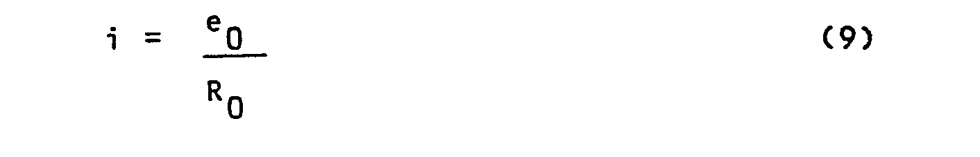
- Thus current i is constant if e0 and R0 are constant.
- Equation (6) is effected by the input and control from resistor 113' to
junction 89 andamplifier 91. - The empirical determination of
resistance wiper 109 is made by placing the circuit elements connected as shown in Figs. 1-6 in an oven, heating the same, and measuring e atjunction 119 and T at ΔT = 0 and at successive temperatures above T . r - Also,


Claims (4)
1. Differential pressure apparatus comprising: a Wheatstone bridge, a first and a second Leg each including a strain gage, a third and fourth Leg each including a resistor, an evaluation circuit with display means connected to the first diagonal branch, a temperature compensated regulated voltage and connected to the second diagonal branch via a first differential amplifier, controlled by the bridge current, characterized in, that the voltage caused by the temperature dependence of the strain gages (148, 149) available at the junction between the first and third Leg is fed via a second differential amplifier (110) to the first differential amplifier (91).
2. Differential pressure apparatus as defined in claim 1, characterized in that the temperature dependent voltage is connected to the noninverting input (+) of the second differential amplifier (110) and its inverting input (-) is connected to a constant voltage (Eb).
3. Differential pressure apparatus as defined in claim 1, characterized in that the output of the second differential amplifier (110) is connected to the noninverting input (+) of the first differential amplifier (91).
4. Differential pressure apparatus as defined in claim 2, characterized in that the gain of the second differential amplifier (110) is adjustable by a variable resistor (112) connected between its output (85) and its inverting input (-).
Applications Claiming Priority (2)
| Application Number | Priority Date | Filing Date | Title |
|---|---|---|---|
| US374972 | 1982-05-05 | ||
| US06/374,972 US4444056A (en) | 1982-05-05 | 1982-05-05 | Temperature compensated circuit |
Publications (2)
| Publication Number | Publication Date |
|---|---|
| EP0093450A2 true EP0093450A2 (en) | 1983-11-09 |
| EP0093450A3 EP0093450A3 (en) | 1984-04-18 |
Family
ID=23478972
Family Applications (1)
| Application Number | Title | Priority Date | Filing Date |
|---|---|---|---|
| EP83104327A Withdrawn EP0093450A3 (en) | 1982-05-05 | 1983-05-02 | Differential pressure apparatus |
Country Status (4)
| Country | Link |
|---|---|
| US (1) | US4444056A (en) |
| EP (1) | EP0093450A3 (en) |
| JP (1) | JPS5926003A (en) |
| CA (1) | CA1190764A (en) |
Cited By (2)
| Publication number | Priority date | Publication date | Assignee | Title |
|---|---|---|---|---|
| EP0341226A2 (en) * | 1988-04-28 | 1989-11-08 | Schrader Automotive Inc. | On-board tire pressure indicating system performing temperature-compensated pressure measurement, and pressure measurement circuitry thereof |
| CN113238602A (en) * | 2021-05-11 | 2021-08-10 | 西南科技大学 | Unbalanced Wheatstone bridge device and determination method thereof |
Families Citing this family (11)
| Publication number | Priority date | Publication date | Assignee | Title |
|---|---|---|---|---|
| US4527583A (en) * | 1983-07-12 | 1985-07-09 | Dresser Industries, Inc. | Electropneumatic transducer system |
| USRE33028E (en) * | 1983-07-12 | 1989-08-22 | Dresser Industries, Inc. | Electropneumatic transducer system |
| US4541988A (en) * | 1983-12-13 | 1985-09-17 | Bacharach Instrument Company | Constant temperature catalytic gas detection instrument |
| GB8407192D0 (en) * | 1984-03-20 | 1984-04-26 | Lucas Ind Plc | Circuit |
| US4883992A (en) * | 1988-09-06 | 1989-11-28 | Delco Electronics Corporation | Temperature compensated voltage generator |
| US5055269A (en) * | 1989-03-06 | 1991-10-08 | Bacharach, Inc | Temperature limited catalytic gas detector apparatus |
| US5568815A (en) * | 1994-11-21 | 1996-10-29 | Becton Dickinson And Company | Self-powered interface circuit for use with a transducer sensor |
| FR2741951B1 (en) * | 1995-12-04 | 1998-02-20 | Europ Propulsion | WHEATSTONE BRIDGE WITH GRADIENT TEMPERATURE COMPENSATION BETWEEN MAIN BRIDGE RESISTORS AND APPLICATION TO A PRESSURE SENSOR WITH EXTENSOMETRIC GAUGES |
| US8910524B2 (en) * | 2011-12-08 | 2014-12-16 | Kulite Semiconductor Products, Inc. | Linked bridge pressure transducer assemblies |
| JP6779932B2 (en) | 2018-03-20 | 2020-11-04 | 株式会社東芝 | Semiconductor device |
| US11747224B1 (en) * | 2022-02-10 | 2023-09-05 | Ati Industrial Automation, Inc. | Quarter-bridge temperature compensation for force/torque sensor |
Citations (5)
| Publication number | Priority date | Publication date | Assignee | Title |
|---|---|---|---|---|
| DE2841491A1 (en) * | 1977-09-28 | 1979-04-05 | Itt Ind Gmbh Deutsche | BRIDGE CIRCUIT WITH STRAIN GAUGE |
| DE2917237A1 (en) * | 1978-04-28 | 1979-11-08 | Burr Brown Res Corp | RESISTANCE REMOTE SWITCHING |
| JPS578425A (en) * | 1980-06-18 | 1982-01-16 | Mitsubishi Electric Corp | Pressure detector |
| EP0053486A2 (en) * | 1980-12-03 | 1982-06-09 | Honeywell Inc. | Stress sensing apparatus |
| EP0071962A1 (en) * | 1981-08-10 | 1983-02-16 | The Foxboro Company | Pressure transmitter employing non-linear temperature compensation |
Family Cites Families (10)
| Publication number | Priority date | Publication date | Assignee | Title |
|---|---|---|---|---|
| US3161821A (en) * | 1962-07-02 | 1964-12-15 | Statham Instrument Inc | Wheatstone bridge transducer circuits with external balancing means |
| US3722264A (en) * | 1971-01-25 | 1973-03-27 | Itt | Transducer and components therefor |
| GB1414144A (en) * | 1972-03-20 | 1975-11-19 | Welwyn Electric Ltd | Strain measuring device |
| US3841150A (en) * | 1973-11-02 | 1974-10-15 | Honeywell Inc | Strain gauge transducer signal conditioning circuitry |
| JPS5219461A (en) * | 1975-08-04 | 1977-02-14 | Masakuni Kanai | Method of treating humic origin material or oil-fat component (25) |
| US4202218A (en) * | 1977-09-28 | 1980-05-13 | International Telephone And Telegraph Corporation | Bridge circuit |
| US4233848A (en) * | 1978-01-06 | 1980-11-18 | Hitachi, Ltd. | Strain gauge pressure transducer apparatus having an improved impedance bridge |
| US4300395A (en) * | 1978-11-08 | 1981-11-17 | Tokyo Shibaura Denki Kabushiki Kaisha | Semiconductor pressure detection device |
| JPS55113904A (en) * | 1979-02-26 | 1980-09-02 | Hitachi Ltd | Method of zero point temperature compensation for strain-electric signal transducer |
| JPS5653404A (en) * | 1979-10-08 | 1981-05-13 | Hitachi Ltd | Nonlinear correction circuit |
-
1982
- 1982-05-05 US US06/374,972 patent/US4444056A/en not_active Expired - Fee Related
-
1983
- 1983-05-02 EP EP83104327A patent/EP0093450A3/en not_active Withdrawn
- 1983-05-04 JP JP58078893A patent/JPS5926003A/en active Pending
- 1983-05-04 CA CA000427443A patent/CA1190764A/en not_active Expired
Patent Citations (5)
| Publication number | Priority date | Publication date | Assignee | Title |
|---|---|---|---|---|
| DE2841491A1 (en) * | 1977-09-28 | 1979-04-05 | Itt Ind Gmbh Deutsche | BRIDGE CIRCUIT WITH STRAIN GAUGE |
| DE2917237A1 (en) * | 1978-04-28 | 1979-11-08 | Burr Brown Res Corp | RESISTANCE REMOTE SWITCHING |
| JPS578425A (en) * | 1980-06-18 | 1982-01-16 | Mitsubishi Electric Corp | Pressure detector |
| EP0053486A2 (en) * | 1980-12-03 | 1982-06-09 | Honeywell Inc. | Stress sensing apparatus |
| EP0071962A1 (en) * | 1981-08-10 | 1983-02-16 | The Foxboro Company | Pressure transmitter employing non-linear temperature compensation |
Non-Patent Citations (1)
| Title |
|---|
| PATENT ABSTRACTS OF JAPAN, vol. 6, no. 66, 27 April 1982; & JP-A-57 008 425 * |
Cited By (3)
| Publication number | Priority date | Publication date | Assignee | Title |
|---|---|---|---|---|
| EP0341226A2 (en) * | 1988-04-28 | 1989-11-08 | Schrader Automotive Inc. | On-board tire pressure indicating system performing temperature-compensated pressure measurement, and pressure measurement circuitry thereof |
| EP0341226A3 (en) * | 1988-04-28 | 1990-04-18 | Schrader Automotive Inc. | On-board tire pressure indicating system performing temperature-compensated pressure measurement, and pressure measurement circuitry thereof |
| CN113238602A (en) * | 2021-05-11 | 2021-08-10 | 西南科技大学 | Unbalanced Wheatstone bridge device and determination method thereof |
Also Published As
| Publication number | Publication date |
|---|---|
| EP0093450A3 (en) | 1984-04-18 |
| JPS5926003A (en) | 1984-02-10 |
| US4444056A (en) | 1984-04-24 |
| CA1190764A (en) | 1985-07-23 |
Similar Documents
| Publication | Publication Date | Title |
|---|---|---|
| US3841150A (en) | Strain gauge transducer signal conditioning circuitry | |
| US4798093A (en) | Apparatus for sensor compensation | |
| US5343755A (en) | Strain gage sensor with integral temperature signal | |
| EP0053486B1 (en) | Stress sensing apparatus | |
| EP0093450A2 (en) | Differential pressure apparatus | |
| CA2145698C (en) | Electronic circuit for a transducer | |
| US4169243A (en) | Remote sensing apparatus | |
| CN101467013A (en) | Method and apparatus for measuring temperature | |
| US4536715A (en) | Linear dual detector opto-isolator circuit | |
| GB1591620A (en) | Signal-conditioning circuits | |
| US6598484B2 (en) | Physical quantity detection device | |
| US4595884A (en) | Transducer amplifier and method | |
| US4190796A (en) | Pressure detecting apparatus having linear output characteristic | |
| US4766655A (en) | Method for fabricating a compensated silicon pressure sensing device | |
| US4611163A (en) | Temperature compensated resistance bridge circuit | |
| US4672853A (en) | Apparatus and method for a pressure-sensitive device | |
| US3906796A (en) | Electronic temperature measuring apparatus | |
| US4196382A (en) | Physical quantities electric transducers temperature compensation circuit | |
| US3161045A (en) | Strain gauge compensation | |
| CA1117598A (en) | Bridge circuit | |
| JPS6255629B2 (en) | ||
| JPS626171B2 (en) | ||
| JP2610736B2 (en) | Amplification compensation circuit of semiconductor pressure sensor | |
| JPH0313537B2 (en) | ||
| JP2948958B2 (en) | Transducer circuit |
Legal Events
| Date | Code | Title | Description |
|---|---|---|---|
| PUAI | Public reference made under article 153(3) epc to a published international application that has entered the european phase |
Free format text: ORIGINAL CODE: 0009012 |
|
| AK | Designated contracting states |
Designated state(s): DE GB NL |
|
| PUAL | Search report despatched |
Free format text: ORIGINAL CODE: 0009013 |
|
| AK | Designated contracting states |
Designated state(s): DE GB NL |
|
| 17P | Request for examination filed |
Effective date: 19840518 |
|
| RAP1 | Party data changed (applicant data changed or rights of an application transferred) |
Owner name: ITT INDUSTRIES INC. |
|
| STAA | Information on the status of an ep patent application or granted ep patent |
Free format text: STATUS: THE APPLICATION HAS BEEN WITHDRAWN |
|
| 18W | Application withdrawn |
Withdrawal date: 19860118 |
|
| RIN1 | Information on inventor provided before grant (corrected) |
Inventor name: ROMO, EDGAR ARTURO |