EP0091376B1 - Lead format for tape automated bonding - Google Patents
Lead format for tape automated bonding Download PDFInfo
- Publication number
- EP0091376B1 EP0091376B1 EP83400687A EP83400687A EP0091376B1 EP 0091376 B1 EP0091376 B1 EP 0091376B1 EP 83400687 A EP83400687 A EP 83400687A EP 83400687 A EP83400687 A EP 83400687A EP 0091376 B1 EP0091376 B1 EP 0091376B1
- Authority
- EP
- European Patent Office
- Prior art keywords
- lead
- electrically conductive
- segments
- forks
- axial
- Prior art date
- Legal status (The legal status is an assumption and is not a legal conclusion. Google has not performed a legal analysis and makes no representation as to the accuracy of the status listed.)
- Expired
Links
Images


Classifications
-
- H—ELECTRICITY
- H10—SEMICONDUCTOR DEVICES; ELECTRIC SOLID-STATE DEVICES NOT OTHERWISE PROVIDED FOR
- H10W—GENERIC PACKAGES, INTERCONNECTIONS, CONNECTORS OR OTHER CONSTRUCTIONAL DETAILS OF DEVICES COVERED BY CLASS H10
- H10W72/00—Interconnections or connectors in packages
- H10W72/071—Connecting or disconnecting
- H10W72/077—Connecting of TAB connectors
-
- H—ELECTRICITY
- H10—SEMICONDUCTOR DEVICES; ELECTRIC SOLID-STATE DEVICES NOT OTHERWISE PROVIDED FOR
- H10W—GENERIC PACKAGES, INTERCONNECTIONS, CONNECTORS OR OTHER CONSTRUCTIONAL DETAILS OF DEVICES COVERED BY CLASS H10
- H10W70/00—Package substrates; Interposers; Redistribution layers [RDL]
- H10W70/40—Leadframes
- H10W70/421—Shapes or dispositions
-
- H—ELECTRICITY
- H10—SEMICONDUCTOR DEVICES; ELECTRIC SOLID-STATE DEVICES NOT OTHERWISE PROVIDED FOR
- H10W—GENERIC PACKAGES, INTERCONNECTIONS, CONNECTORS OR OTHER CONSTRUCTIONAL DETAILS OF DEVICES COVERED BY CLASS H10
- H10W70/00—Package substrates; Interposers; Redistribution layers [RDL]
- H10W70/40—Leadframes
- H10W70/453—Leadframes comprising flexible metallic tapes
-
- H—ELECTRICITY
- H10—SEMICONDUCTOR DEVICES; ELECTRIC SOLID-STATE DEVICES NOT OTHERWISE PROVIDED FOR
- H10W—GENERIC PACKAGES, INTERCONNECTIONS, CONNECTORS OR OTHER CONSTRUCTIONAL DETAILS OF DEVICES COVERED BY CLASS H10
- H10W72/00—Interconnections or connectors in packages
- H10W72/701—Tape-automated bond [TAB] connectors
-
- H—ELECTRICITY
- H05—ELECTRIC TECHNIQUES NOT OTHERWISE PROVIDED FOR
- H05K—PRINTED CIRCUITS; CASINGS OR CONSTRUCTIONAL DETAILS OF ELECTRIC APPARATUS; MANUFACTURE OF ASSEMBLAGES OF ELECTRICAL COMPONENTS
- H05K1/00—Printed circuits
- H05K1/02—Details
- H05K1/0271—Arrangements for reducing stress or warp in rigid printed circuit boards, e.g. caused by loads, vibrations or differences in thermal expansion
-
- Y—GENERAL TAGGING OF NEW TECHNOLOGICAL DEVELOPMENTS; GENERAL TAGGING OF CROSS-SECTIONAL TECHNOLOGIES SPANNING OVER SEVERAL SECTIONS OF THE IPC; TECHNICAL SUBJECTS COVERED BY FORMER USPC CROSS-REFERENCE ART COLLECTIONS [XRACs] AND DIGESTS
- Y10—TECHNICAL SUBJECTS COVERED BY FORMER USPC
- Y10T—TECHNICAL SUBJECTS COVERED BY FORMER US CLASSIFICATION
- Y10T428/00—Stock material or miscellaneous articles
- Y10T428/12—All metal or with adjacent metals
- Y10T428/12229—Intermediate article [e.g., blank, etc.]
-
- Y—GENERAL TAGGING OF NEW TECHNOLOGICAL DEVELOPMENTS; GENERAL TAGGING OF CROSS-SECTIONAL TECHNOLOGIES SPANNING OVER SEVERAL SECTIONS OF THE IPC; TECHNICAL SUBJECTS COVERED BY FORMER USPC CROSS-REFERENCE ART COLLECTIONS [XRACs] AND DIGESTS
- Y10—TECHNICAL SUBJECTS COVERED BY FORMER USPC
- Y10T—TECHNICAL SUBJECTS COVERED BY FORMER US CLASSIFICATION
- Y10T428/00—Stock material or miscellaneous articles
- Y10T428/12—All metal or with adjacent metals
- Y10T428/12361—All metal or with adjacent metals having aperture or cut
Definitions
- the present invention relates generally to packages for integrated circuits, and more particularly to a lead frame format which allows inner lead attachment to a die prior to outer lead attachment to a substrate.
- silicon wafers containing many separate integrated circuits are fabricated and then cut into individual circuits, each known as a die.
- Each die is individually packaged, using any one of a variety of known techniques.
- electrically conductive leads are attached to the die, typically by well-known techniques, such as wire bonding or tape-automated bonding.
- the assembly of the die and the conductive leads is then usually encapsulated in epoxy or some other enclosure for protection.
- Tape-automated bonding is a technique for interconnecting an integrated circuit to leads fabricated on a continuous carrier film.
- the tape is typically a laminate of copper and a plastic insulator, and the leads are etched in the copper while on the plastic carrier using conventional techniques.
- the film is perforated along one or both edges with sprocket holes used for advancement and registration.
- Each pattern of leads referred to as a frame, includes a central window or opening through the carrier film.
- the inner ends of the leads overhang the central opening and may be mass bonded to an integrated circuit which is brought into close proximity with the opening, typically by thermocompression, ultrasonic, eutectic, or reflow solder techniques.
- the outer portion of each lead is connected to a substrate onto which the die is also mounted, and the plastic carrier is excised from the leads prior to final packaging of the device.
- One such testing method is achieved by first bonding the inner ends of the individual leads to the integrated circuit. The circuit is then carried by the carrier film to a testing station where a conventional probe may be attached to the circuit. After the circuit has been tested and found to meet specifications, the device may be bonded to a substrate by conventional means.
- each lead must have the ability to stretch as the offset introduced by the thickness of the integrated circuit changes the distance between the inner bonding point of the lead and the position of the outer lead on the tape.
- Leads including rectangular stretch loops are disclosed in British patent GB-A-1483322.
- the amount of extension of the lead is limited by the distance d between the sides of the loop. In other words, for a desired amount of extension, the width d of the loop must be greater than a given value.
- the present invention provides a novel stretch loop which allows close packing of the leads for high lead count devices and in which the amount of extension is not limited by the width of the stretch loop.
- Another aspect of the invention includes a tape for use in tape automated bonding according to claim 10.
- a tape 10 comprises a plurality of electrically-conductive leads 12 laminated to the underside (as viewed in Fig. 1) of a carrier film 14.
- the leads 12 are typically formed from copper, and conventional circuit board processes are used to etch a copper layer laminated to the film 14 into the desired pattern of leads.
- the film 14 is typically formed from glass fiber or a synthetic polymer. It is desirable that the polymer be heat and chemical resistant to withstand the various processing steps required in formation of the tape and connection of the leads 12 to an integrated circuit 26.
- Preferred polymers include MylariID (polyester), and polyvinyl chloride. Par- tiuclarly preferred are polyimides.
- the film 14 includes sprocket holes 16 along both edges for use in advancement and registration of the film.
- the tape 10 includes a plurality of frames 20 defined by a central opening 22 penetrating the carrier film 14 at a location typically mid-way between the edges.
- the frame 20 is further defined by the plurality of leads 12 which encompass the periphery of the opening 22, each extending inward a short distance into the opening.
- the portion 24 of each lead 12 which extends into the opening 22 is eventually bonded to the integrated circuit die 26 which is brought into position beneath the opening 22.
- the integrated circuit die 26 is bonded to a substrate 28 in a multi-step operation, as will now be described.
- the integrated circuit 26 is held in a wax form 30, illustrated in Fig. 2A.
- the integrated circuit 26 is brought into contact with the tape 10 at the appropriate frame 20 so that the inwardly extending portions 24 of the leads 12 contact bumps 32 formed on the upper surface (as viewed in the Drawings) of the circuit 26.
- the inwardly extending portions 24 of the leads 12 contact bumps 32 formed on the upper surface (as viewed in the Drawings) of the circuit 26.
- the integrated circuit 26 includes a plurality of bumps 32 corresponding to the number of electrical contacts in the particular integrated circuit, and that for the most part each bump 32 will have a corresponding electrical lead 12 to which it will be attached.
- the bumps 32 are typically formed from a gold/tin alloy which may be thermally bonded to the leads 12 in a conventional manner, typically by thermocompression, ultrasonic, eutectic or reflow solder techniques. The heat from the bonding will melt the wax form 30 and allow the tape 10 to carry the die 26 upward and away.
- the circuit may be tested by a conventional techniques. Testing at this stage of assembly is particularly convenient since the circuits are still mounted on the tape and may be sequentially screened as part of the assembly procedure. Moreover, the .circuits have been bonded to the lead frame and any damage which may have resulted from such handling and bonding will be uncovered in the screening.
- the circuit will be typically mounted on the substrate 28 to form a conventional package. As shown in Fig. 2B, the circuit 26 is brought into position so that it lies adjacent the proper position on the substrate 28 and is connected using any conventional technique. Typically, a thin layer of conductive polyimide paste is placed on the substrate and the entire assembly is heated sufficiently to cure the paste and secure the die 26 to the substrate 28.
- the leads 12 will be formed downward and attached to the substrate 28, as illustrated in Fig. 2C.
- the outer portions of the leads 12 are bonded to the substrate 28 by conventional means, typically using gold-tin reflow techniques. It is preferred to form the leads 12 and bond both the leads and the die 26 to the substrate 28 in a single step, although the order and manner of bonding the various components is not critical.
- stretch loops 40 are provided in the inner portions 24 of each lead 12 so that the lead is capable of elongating as the lead is formed downward onto the substrate 28.
- each lead 12 is vertically offset as the outer portion of the lead is pressed downward and bonded to the substrate 28. Since the inner portion 24 of the lead 12 has already been bonded to the metalic bump 32, and the outer portion is laminated to the carrier film 14, the lead must include a portion which is capable of stretching to accommodate the vertical displacement.
- Outer lead bonds may be formed and the package completed in a conventional manner.
- the present invention is directed at a lead format which incorporates particular stetch loops which allow bonding of the lead frame to the integrated circuit prior to bonding the remainder of the frame to an offset substrate.
- the stretch loops of the present invention minimize the necessary spacing between adjacent leads to allow close packing of the leads and a correspondingly high lead count in the resulting package.
- prior art lead frames 40a were formed as rectangles having a pair of laterally extending segments 42 extending from each of two forks 44 formed in the lead 12.
- the laterally extending segments 42 are joined by axially aligned segments 46 to complete the rectangle.
- the rectangle collapses causing segments 42 to realign in the axial direction.
- extension of the prior art loop 40a is limited to a distance equal to approximately twice the length of the segments 42, and for a given extension requirement, adjacent leads 12 can be spaced no closer than one-half the length of the extension.
- the stretch loop of the present invention allows adjacent leads to be closely spaced for connection to high density integrated circuits having connection points which are closely spaced apart. It accomplishes this by providing a stretch loop having a plurality of segments wherein the segments which contribute to the elongation are axially aligned rather than oriented, as in the prior art.
- a first embodiment 40b of the stretch loop comprises a pair of branches 50 which connect to forks 52 formed in each lead 12.
- Each branch includes a first segment 54 which is axially aligned with the lead 12 and connected to the lead by a pair of segments 56 which are also axially aligned with lead 12 and located between the lead and the first segment 54.
- the first segment 54 is connected at each end to the other segments 56 by short, arcuate sections 58.
- the interior ends of the segments 56 are connected to the forks 52 by arcuate sections 60.
- the width of the leads 12 will typically be in the range from 254 pm to 762 pm (10 to 30 mils), depending on the density, more typically in the range from 504 ⁇ m to 635 ⁇ m (20 to 25 mils).
- the width of the branches 50 will be approximately one-half the width of the lead, although the width may vary at points, typically narrowing through the arcuate sections 58, 60 to facilitate unfolding.
- the radius of such arcuate sections 58, 60 is preferably made as small as possible consistent with maintaining the ability to unfold.
- the inner radius r, (Fig. 4A) will typically be less than one-half the width of the branch 70, more typically less than one-quarter such width.
- the arcuate sections 58 and 60 may have non-circular profiles, the only requirement being that such segments allow the loop 40b to unfold as the lead 12 is elongated.
- Figs. 4A-4D as the lead 12 is offset during bonding to the substrate, an axial tension is experienced by the lead which draws the forks 52 apart.
- segments 56 move from an axial alignment to a lateral alignment, as shown in Fig. 4C.
- the first segments 54 move laterally away from the centre line of the lead 12, typically contacting and sliding by the adjacent lead.
- the segments 54 are drawn back toward the center and the lead 12 assumes a final configuration, as illustrated in Fig. 4D.
- the length of the first segment 54 can be increased as described to increase the ultimate amount by which the loop 40b can elongate.
- a stretch loop 40c comprises a pair of forks 68 formed in the lead 12.
- Each fork 68 defines two branches 70, said branches extending between the forks.
- the forks 68 are spaced-apart a predetermined distance in the axial direction, and each branch 70 includes a first axial segment 72 having a length slightly less than said distance.
- the branch 70 is completed by additional axially aligned segments 74 and 76 which connect each end of the first segment 72 to the forks 68.
- the width of each branch 72 is approximately one-half that of the lead 12 and, by closely spacing the various axial segments, it will be seen that the total width of the stretch loop 46c may approach as low as three times the width of the lead 12. This is true even though a total elongation equal to ten times the width of the lead, or more, may be provided.
- the various axial segments 72, 74 and 76 of the branches 70 are connected by short, arcuate sections 78 and 80, as illustrated.
- the width of these sections will typically be somewhat less than that of the branches 70, to facilitate unfolding of the loop 40c.
- the first axially aligned segments 72 unfold inward (as illustrated in Figs. 5A-5E) to avoid interference between adjacent leads 12. If section 78 were stronger (i.e., more resistant to unfolding) than section 82 which defines the transition from the forks 68 to the segments 76, the loop 40c would initially unfold as indicated by arrows 84 (Fig. 5A), causing undesirable interference between adjacent leads 12.
- stretch loops 40 located on adjacent leads be axially staggered to allow the closest possible packing of the leads.
- the leads may be spaced apart a distance approximately equal to the width of one branch of the stretch loop, rather than twice the width as would be required if the loops were placed laterally adjacent.
Landscapes
- Wire Bonding (AREA)
Description
- The present invention relates generally to packages for integrated circuits, and more particularly to a lead frame format which allows inner lead attachment to a die prior to outer lead attachment to a substrate.
- In the manufacture of integrated circuits, silicon wafers containing many separate integrated circuits are fabricated and then cut into individual circuits, each known as a die. Each die is individually packaged, using any one of a variety of known techniques. During packaging, electrically conductive leads are attached to the die, typically by well-known techniques, such as wire bonding or tape-automated bonding. The assembly of the die and the conductive leads is then usually encapsulated in epoxy or some other enclosure for protection.
- Tape-automated bonding is a technique for interconnecting an integrated circuit to leads fabricated on a continuous carrier film. The tape is typically a laminate of copper and a plastic insulator, and the leads are etched in the copper while on the plastic carrier using conventional techniques. The film is perforated along one or both edges with sprocket holes used for advancement and registration.
- Each pattern of leads, referred to as a frame, includes a central window or opening through the carrier film. The inner ends of the leads overhang the central opening and may be mass bonded to an integrated circuit which is brought into close proximity with the opening, typically by thermocompression, ultrasonic, eutectic, or reflow solder techniques. The outer portion of each lead is connected to a substrate onto which the die is also mounted, and the plastic carrier is excised from the leads prior to final packaging of the device.
- It is desirable to test the individual integrated circuits prior to final packaging. It is particularly desirable to test the devices while still attached to the plastic carrier film and prior to final attachment of the lead frame to the substrate. One such testing method is achieved by first bonding the inner ends of the individual leads to the integrated circuit. The circuit is then carried by the carrier film to a testing station where a conventional probe may be attached to the circuit. After the circuit has been tested and found to meet specifications, the device may be bonded to a substrate by conventional means.
- Typically, the outer portions of the leads (which are still attached to the carrier film) are formed downward and bonded to the substrate while the inner ends of the lead remain attached to the die. Thus, each lead must have the ability to stretch as the offset introduced by the thickness of the integrated circuit changes the distance between the inner bonding point of the lead and the position of the outer lead on the tape.
- Heretofore, the ability to stretch has been provided by a stretch loop comprising a rectangular segment built into the lead, which loop collapses as the lead is elongated by the offset (see Figure 3). While generally successful, such rectangular stretch loops are much wider than the lead itself and thus prevent close packing of the leads, which inhibits the application of the above-described technique on high lead count devices.
- Leads including rectangular stretch loops are disclosed in British patent GB-A-1483322. When these stretch loops are used, the amount of extension of the lead is limited by the distance d between the sides of the loop. In other words, for a desired amount of extension, the width d of the loop must be greater than a given value.
- The present invention provides a novel stretch loop which allows close packing of the leads for high lead count devices and in which the amount of extension is not limited by the width of the stretch loop.
- This and other objects are attained according to the invention by the electrically conductive lead of claim 1.
- Another aspect of the invention includes a tape for use in tape automated bonding according to
claim 10. -
- Fig. 1 is a view of a tape comprising a carrier film having the leads of the present invention positioned above an integrated circuit prior to bonding of the leads to a substrate.
- Figs. 2A-2C are partial elevational views illustrating the elongation of the stretch loop of the present invention when the lead is offset.
- Fig. 3 illustrates the prior art stretch loop.
- Fig. 4 illustrates a first embodiment of the stretch loop of the present invention.
- Fig. 4A illustrates an arcuate connecting section in detail.
- Figs. 4B-4D illustrate the manner in which the stretch loop of Fig. 4 unfolds as the lead is elongated.
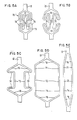
- Fig. 5 illustrates a second embodiment of the stretch loop of the present invention.
- Figs. 5A-5E illustrate the manner in which the stretch loop of Fig. 5 unfolds as the lead is elongated.
- Referring to Fig. 1, a
tape 10 comprises a plurality of electrically-conductive leads 12 laminated to the underside (as viewed in Fig. 1) of acarrier film 14. Theleads 12 are typically formed from copper, and conventional circuit board processes are used to etch a copper layer laminated to thefilm 14 into the desired pattern of leads. Thefilm 14 is typically formed from glass fiber or a synthetic polymer. It is desirable that the polymer be heat and chemical resistant to withstand the various processing steps required in formation of the tape and connection of theleads 12 to an integratedcircuit 26. Preferred polymers include MylariID (polyester), and polyvinyl chloride. Par- tiuclarly preferred are polyimides. Thefilm 14 includessprocket holes 16 along both edges for use in advancement and registration of the film. - The
tape 10 includes a plurality offrames 20 defined by acentral opening 22 penetrating thecarrier film 14 at a location typically mid-way between the edges. Theframe 20 is further defined by the plurality ofleads 12 which encompass the periphery of theopening 22, each extending inward a short distance into the opening. As will be described in more detail hereinafter, theportion 24 of eachlead 12 which extends into the opening 22 is eventually bonded to the integratedcircuit die 26 which is brought into position beneath the opening 22. - Referring to Figs. 2A-2D, the
integrated circuit die 26 is bonded to asubstrate 28 in a multi-step operation, as will now be described. Initially, the integratedcircuit 26 is held in awax form 30, illustrated in Fig. 2A. The integratedcircuit 26 is brought into contact with thetape 10 at theappropriate frame 20 so that the inwardly extendingportions 24 of theleads 12contact bumps 32 formed on the upper surface (as viewed in the Drawings) of thecircuit 26. Although only asingle lead 12 andbump 32 are illustrated in Figs. 2A-2D, it is to be understood that theintegrated circuit 26 includes a plurality ofbumps 32 corresponding to the number of electrical contacts in the particular integrated circuit, and that for the most part eachbump 32 will have a correspondingelectrical lead 12 to which it will be attached. Thebumps 32 are typically formed from a gold/tin alloy which may be thermally bonded to theleads 12 in a conventional manner, typically by thermocompression, ultrasonic, eutectic or reflow solder techniques. The heat from the bonding will melt thewax form 30 and allow thetape 10 to carry thedie 26 upward and away. - After the integrated
circuit 26 has been bonded to theleads 12, and before the circuit is mounted on the substrate 28 (as will be shown hereinafter), the circuit may be tested by a conventional techniques. Testing at this stage of assembly is particularly convenient since the circuits are still mounted on the tape and may be sequentially screened as part of the assembly procedure. Moreover, the .circuits have been bonded to the lead frame and any damage which may have resulted from such handling and bonding will be uncovered in the screening. - After the
integrated circuit 26 has been tested and found functional, the circuit will be typically mounted on thesubstrate 28 to form a conventional package. As shown in Fig. 2B, thecircuit 26 is brought into position so that it lies adjacent the proper position on thesubstrate 28 and is connected using any conventional technique. Typically, a thin layer of conductive polyimide paste is placed on the substrate and the entire assembly is heated sufficiently to cure the paste and secure the die 26 to thesubstrate 28. - Conveniently, before the assembly of the
substrate 28 and thedie 26 is heated, theleads 12 will be formed downward and attached to thesubstrate 28, as illustrated in Fig. 2C. The outer portions of theleads 12 are bonded to thesubstrate 28 by conventional means, typically using gold-tin reflow techniques. It is preferred to form theleads 12 and bond both the leads and the die 26 to thesubstrate 28 in a single step, although the order and manner of bonding the various components is not critical. - Referring now to both Figs. 1 and 2A-2D,
stretch loops 40 are provided in theinner portions 24 of each lead 12 so that the lead is capable of elongating as the lead is formed downward onto thesubstrate 28. As best observed in Figs. 2B and 2C, each lead 12 is vertically offset as the outer portion of the lead is pressed downward and bonded to thesubstrate 28. Since theinner portion 24 of thelead 12 has already been bonded to themetalic bump 32, and the outer portion is laminated to thecarrier film 14, the lead must include a portion which is capable of stretching to accommodate the vertical displacement. - After the outer portions of the
leads 12 have been bonded to thesubstrate 28, thecarrier film 14 is excised, leaving the package as illustrated in Fig. 2D. Outer lead bonds may be formed and the package completed in a conventional manner. - The present invention is directed at a lead format which incorporates particular stetch loops which allow bonding of the lead frame to the integrated circuit prior to bonding the remainder of the frame to an offset substrate. The stretch loops of the present invention minimize the necessary spacing between adjacent leads to allow close packing of the leads and a correspondingly high lead count in the resulting package.
- Referring now to Fig. 3, prior art lead frames 40a were formed as rectangles having a pair of laterally extending
segments 42 extending from each of twoforks 44 formed in thelead 12. The laterally extendingsegments 42 are joined by axially alignedsegments 46 to complete the rectangle. As thelead 12 is extended, the rectangle collapses causingsegments 42 to realign in the axial direction. Thus, extension of theprior art loop 40a is limited to a distance equal to approximately twice the length of thesegments 42, and for a given extension requirement, adjacent leads 12 can be spaced no closer than one-half the length of the extension. - The stretch loop of the present invention allows adjacent leads to be closely spaced for connection to high density integrated circuits having connection points which are closely spaced apart. It accomplishes this by providing a stretch loop having a plurality of segments wherein the segments which contribute to the elongation are axially aligned rather than oriented, as in the prior art.
- Referring to Fig. 4, a
first embodiment 40b of the stretch loop comprises a pair ofbranches 50 which connect toforks 52 formed in each lead 12. Each branch includes afirst segment 54 which is axially aligned with thelead 12 and connected to the lead by a pair ofsegments 56 which are also axially aligned withlead 12 and located between the lead and thefirst segment 54. Thefirst segment 54 is connected at each end to theother segments 56 by short,arcuate sections 58. Similarly, the interior ends of thesegments 56 are connected to theforks 52 byarcuate sections 60. - The width of the
leads 12 will typically be in the range from 254 pm to 762 pm (10 to 30 mils), depending on the density, more typically in the range from 504 µm to 635 µm (20 to 25 mils). The width of thebranches 50 will be approximately one-half the width of the lead, although the width may vary at points, typically narrowing through thearcuate sections arcuate sections branch 70, more typically less than one-quarter such width. Moreover, thearcuate sections loop 40b to unfold as thelead 12 is elongated. - Referring now also to Figs. 4A-4D, as the
lead 12 is offset during bonding to the substrate, an axial tension is experienced by the lead which draws theforks 52 apart. As theforks 52 move apart,segments 56 move from an axial alignment to a lateral alignment, as shown in Fig. 4C. As this occurs, thefirst segments 54 move laterally away from the centre line of thelead 12, typically contacting and sliding by the adjacent lead. As theforks 52 continue to move apart, thesegments 54 are drawn back toward the center and thelead 12 assumes a final configuration, as illustrated in Fig. 4D. The length of thefirst segment 54 can be increased as described to increase the ultimate amount by which theloop 40b can elongate. - An alternate embodiment is illustrated in Fig. 5. A stretch loop 40c comprises a pair of
forks 68 formed in thelead 12. Eachfork 68 defines twobranches 70, said branches extending between the forks. Theforks 68 are spaced-apart a predetermined distance in the axial direction, and eachbranch 70 includes a firstaxial segment 72 having a length slightly less than said distance. Thebranch 70 is completed by additional axially alignedsegments first segment 72 to theforks 68. Again, the width of eachbranch 72 is approximately one-half that of thelead 12 and, by closely spacing the various axial segments, it will be seen that the total width of the stretch loop 46c may approach as low as three times the width of thelead 12. This is true even though a total elongation equal to ten times the width of the lead, or more, may be provided. - The various
axial segments branches 70 are connected by short,arcuate sections branches 70, to facilitate unfolding of the loop 40c. Moreover, by assuring that the loop 40c unfolds initially atsections 78 and 80 (typically by narrowing these sections relative to the remainder of the branch), the first axially alignedsegments 72 unfold inward (as illustrated in Figs. 5A-5E) to avoid interference between adjacent leads 12. Ifsection 78 were stronger (i.e., more resistant to unfolding) thansection 82 which defines the transition from theforks 68 to thesegments 76, the loop 40c would initially unfold as indicated by arrows 84 (Fig. 5A), causing undesirable interference between adjacent leads 12. - As illustrated in both Figs. 4and 5, it is desirable that
stretch loops 40 located on adjacent leads be axially staggered to allow the closest possible packing of the leads. By staggering, the leads may be spaced apart a distance approximately equal to the width of one branch of the stretch loop, rather than twice the width as would be required if the loops were placed laterally adjacent.
Claims (11)
Applications Claiming Priority (2)
| Application Number | Priority Date | Filing Date | Title |
|---|---|---|---|
| US06/365,686 US4390598A (en) | 1982-04-05 | 1982-04-05 | Lead format for tape automated bonding |
| US365686 | 1982-04-05 |
Publications (2)
| Publication Number | Publication Date |
|---|---|
| EP0091376A1 EP0091376A1 (en) | 1983-10-12 |
| EP0091376B1 true EP0091376B1 (en) | 1987-01-21 |
Family
ID=23439911
Family Applications (1)
| Application Number | Title | Priority Date | Filing Date |
|---|---|---|---|
| EP83400687A Expired EP0091376B1 (en) | 1982-04-05 | 1983-04-01 | Lead format for tape automated bonding |
Country Status (5)
| Country | Link |
|---|---|
| US (1) | US4390598A (en) |
| EP (1) | EP0091376B1 (en) |
| JP (2) | JPS58184752A (en) |
| DE (1) | DE3369430D1 (en) |
| PH (1) | PH21455A (en) |
Families Citing this family (23)
| Publication number | Priority date | Publication date | Assignee | Title |
|---|---|---|---|---|
| US4688075A (en) * | 1983-07-22 | 1987-08-18 | Fairchild Semiconductor Corporation | Integrated circuit having a pre-attached conductive mounting media and method of making the same |
| US4571354A (en) * | 1983-12-27 | 1986-02-18 | Rogers Corporation | Tape automated bonding of integrated circuits |
| GB2167228B (en) * | 1984-10-11 | 1988-05-05 | Anamartic Ltd | Integrated circuit package |
| US4721993A (en) * | 1986-01-31 | 1988-01-26 | Olin Corporation | Interconnect tape for use in tape automated bonding |
| US4800419A (en) * | 1987-01-28 | 1989-01-24 | Lsi Logic Corporation | Support assembly for integrated circuits |
| US4771330A (en) * | 1987-05-13 | 1988-09-13 | Lsi Logic Corporation | Wire bonds and electrical contacts of an integrated circuit device |
| US4855672A (en) * | 1987-05-18 | 1989-08-08 | Shreeve Robert W | Method and process for testing the reliability of integrated circuit (IC) chips and novel IC circuitry for accomplishing same |
| US4918385A (en) * | 1987-05-18 | 1990-04-17 | Hewlett-Packard Company | Method and process for testing the reliability of integrated circuit (IC) chips and novel IC circuitry for accomplishing same |
| US4980753A (en) * | 1988-11-21 | 1990-12-25 | Honeywell Inc. | Low-cost high-performance semiconductor chip package |
| US5061988A (en) * | 1990-07-30 | 1991-10-29 | Mcdonnell Douglas Corporation | Integrated circuit chip interconnect |
| US7198969B1 (en) | 1990-09-24 | 2007-04-03 | Tessera, Inc. | Semiconductor chip assemblies, methods of making same and components for same |
| US5065504A (en) * | 1990-11-05 | 1991-11-19 | Microelectronics And Computer Technology Corporation | Method of forming flexible metal leads on integrated circuits |
| MY107849A (en) * | 1991-09-09 | 1996-06-29 | Hitachi Cable | Composite lead frame and method for manufacturing the same. |
| US5210936A (en) * | 1992-01-06 | 1993-05-18 | Microelectronics And Computer Technology Corporation | Method and apparatus for the excise and lead form of TAB devices |
| US5567654A (en) * | 1994-09-28 | 1996-10-22 | International Business Machines Corporation | Method and workpiece for connecting a thin layer to a monolithic electronic module's surface and associated module packaging |
| JP2767404B2 (en) * | 1994-12-14 | 1998-06-18 | アナムインダストリアル株式会社 | Lead frame structure of semiconductor package |
| JP3170182B2 (en) * | 1995-08-15 | 2001-05-28 | 株式会社東芝 | Resin-sealed semiconductor device and method of manufacturing the same |
| DE19717780A1 (en) * | 1996-05-01 | 1997-11-13 | Nat Semiconductor Corp | Conductive frame for semiconductor components |
| JP4349541B2 (en) * | 2000-05-09 | 2009-10-21 | 大日本印刷株式会社 | Resin-encapsulated semiconductor device frame |
| US20040105244A1 (en) * | 2002-08-06 | 2004-06-03 | Ilyas Mohammed | Lead assemblies with offset portions and microelectronic assemblies with leads having offset portions |
| US7132734B2 (en) * | 2003-01-06 | 2006-11-07 | Micron Technology, Inc. | Microelectronic component assemblies and microelectronic component lead frame structures |
| US7183485B2 (en) | 2003-03-11 | 2007-02-27 | Micron Technology, Inc. | Microelectronic component assemblies having lead frames adapted to reduce package bow |
| US7466012B2 (en) | 2004-09-13 | 2008-12-16 | International Rectifier Corporation | Power semiconductor package |
Family Cites Families (8)
| Publication number | Priority date | Publication date | Assignee | Title |
|---|---|---|---|---|
| US3422213A (en) * | 1966-04-21 | 1969-01-14 | Webb James E | Connector strips |
| US3519890A (en) * | 1968-04-01 | 1970-07-07 | North American Rockwell | Low stress lead |
| DE7045153U (en) * | 1970-12-07 | 1972-04-13 | Nat Beryllia Corp | LADDER EXECUTION |
| US3947867A (en) * | 1970-12-21 | 1976-03-30 | Signetics Corporation | Two part package for a semiconductor die |
| US3905038A (en) * | 1973-02-26 | 1975-09-09 | Signetics Corp | Semiconductor assembly and method |
| US3809800A (en) * | 1973-04-25 | 1974-05-07 | Nasa | Means for accommodating large overstrain in lead wires |
| FR2299724A1 (en) * | 1975-01-29 | 1976-08-27 | Honeywell Bull Soc Ind | IMPROVEMENTS TO PACKAGING MEDIA FOR INTEGRATED CIRCUIT BOARDS |
| US4331740A (en) * | 1980-04-14 | 1982-05-25 | National Semiconductor Corporation | Gang bonding interconnect tape process and structure for semiconductor device automatic assembly |
-
1982
- 1982-04-05 US US06/365,686 patent/US4390598A/en not_active Expired - Lifetime
-
1983
- 1983-04-01 EP EP83400687A patent/EP0091376B1/en not_active Expired
- 1983-04-01 DE DE8383400687T patent/DE3369430D1/en not_active Expired
- 1983-04-04 PH PH28732A patent/PH21455A/en unknown
- 1983-04-05 JP JP58058840A patent/JPS58184752A/en active Granted
-
1989
- 1989-12-27 JP JP1336827A patent/JPH03114242A/en active Granted
Also Published As
| Publication number | Publication date |
|---|---|
| EP0091376A1 (en) | 1983-10-12 |
| JPH03114242A (en) | 1991-05-15 |
| JPH0231862B2 (en) | 1990-07-17 |
| JPH0416942B2 (en) | 1992-03-25 |
| PH21455A (en) | 1987-10-28 |
| DE3369430D1 (en) | 1987-02-26 |
| JPS58184752A (en) | 1983-10-28 |
| US4390598A (en) | 1983-06-28 |
Similar Documents
| Publication | Publication Date | Title |
|---|---|---|
| US4390598A (en) | Lead format for tape automated bonding | |
| KR930010086B1 (en) | Semiconductor integrated circuit device | |
| EP0676091B1 (en) | Tab testing of area array interconnected chips | |
| US7002240B2 (en) | Semiconductor leadframe for staggered board attach | |
| KR100241573B1 (en) | Semiconductor wafer | |
| US5994768A (en) | Multi-layer lead frame | |
| US20100084748A1 (en) | Thin foil for use in packaging integrated circuits | |
| KR100926002B1 (en) | Semiconductor package device and method of formation and testing | |
| US5926695A (en) | Lead frame incorporating material flow diverters | |
| KR980012316A (en) | Semiconductor device and manufacturing method thereof | |
| KR0185570B1 (en) | Manufacturing method of chip scale package | |
| US4951120A (en) | Lead frame and semiconductor device using the same | |
| US6037662A (en) | Chip scale package | |
| US5704593A (en) | Film carrier tape for semiconductor package and semiconductor device employing the same | |
| US4688075A (en) | Integrated circuit having a pre-attached conductive mounting media and method of making the same | |
| US6495400B1 (en) | Method of forming low profile semiconductor package | |
| US5408127A (en) | Method of and arrangement for preventing bonding wire shorts with certain integrated circuit components | |
| KR100198682B1 (en) | Semiconductor device manufacturing method | |
| KR100658120B1 (en) | Process for manufacturing semiconductor device using film substrate | |
| US6353259B1 (en) | Process for producing BGA type semiconductor device, TAB tape for BGA type semiconductor device, and BGA type semiconductor device | |
| GB2247988A (en) | Lead frame for semiconductor device | |
| EP0204102A2 (en) | Direct connection of lead frame having flexible, tapered leads and mechanical die support | |
| JPH0834282B2 (en) | Lead frame for semiconductor device | |
| JPH05226422A (en) | Film carrier tape | |
| JPH08204062A (en) | Ball grid array type semiconductor device and method of manufacturing the same |
Legal Events
| Date | Code | Title | Description |
|---|---|---|---|
| PUAI | Public reference made under article 153(3) epc to a published international application that has entered the european phase |
Free format text: ORIGINAL CODE: 0009012 |
|
| AK | Designated contracting states |
Designated state(s): DE FR GB IT NL |
|
| 17P | Request for examination filed |
Effective date: 19840404 |
|
| GRAA | (expected) grant |
Free format text: ORIGINAL CODE: 0009210 |
|
| ITF | It: translation for a ep patent filed | ||
| AK | Designated contracting states |
Kind code of ref document: B1 Designated state(s): DE FR GB IT NL |
|
| REF | Corresponds to: |
Ref document number: 3369430 Country of ref document: DE Date of ref document: 19870226 |
|
| ET | Fr: translation filed | ||
| PLBE | No opposition filed within time limit |
Free format text: ORIGINAL CODE: 0009261 |
|
| STAA | Information on the status of an ep patent application or granted ep patent |
Free format text: STATUS: NO OPPOSITION FILED WITHIN TIME LIMIT |
|
| 26N | No opposition filed | ||
| ITTA | It: last paid annual fee | ||
| PGFP | Annual fee paid to national office [announced via postgrant information from national office to epo] |
Ref country code: GB Payment date: 19940321 Year of fee payment: 12 |
|
| PGFP | Annual fee paid to national office [announced via postgrant information from national office to epo] |
Ref country code: FR Payment date: 19940412 Year of fee payment: 12 |
|
| PGFP | Annual fee paid to national office [announced via postgrant information from national office to epo] |
Ref country code: NL Payment date: 19940430 Year of fee payment: 12 |
|
| PG25 | Lapsed in a contracting state [announced via postgrant information from national office to epo] |
Ref country code: GB Effective date: 19950401 |
|
| PG25 | Lapsed in a contracting state [announced via postgrant information from national office to epo] |
Ref country code: NL Effective date: 19951101 |
|
| GBPC | Gb: european patent ceased through non-payment of renewal fee |
Effective date: 19950401 |
|
| PG25 | Lapsed in a contracting state [announced via postgrant information from national office to epo] |
Ref country code: FR Effective date: 19951229 |
|
| NLV4 | Nl: lapsed or anulled due to non-payment of the annual fee |
Effective date: 19951101 |
|
| REG | Reference to a national code |
Ref country code: FR Ref legal event code: ST |
|
| PGFP | Annual fee paid to national office [announced via postgrant information from national office to epo] |
Ref country code: DE Payment date: 19960430 Year of fee payment: 14 |
|
| PG25 | Lapsed in a contracting state [announced via postgrant information from national office to epo] |
Ref country code: DE Free format text: LAPSE BECAUSE OF NON-PAYMENT OF DUE FEES Effective date: 19980101 |