EP0091333B1 - Dispositif de protection de la commande de balayage horizontal d'un écran de visualisation - Google Patents
Dispositif de protection de la commande de balayage horizontal d'un écran de visualisation Download PDFInfo
- Publication number
- EP0091333B1 EP0091333B1 EP83400535A EP83400535A EP0091333B1 EP 0091333 B1 EP0091333 B1 EP 0091333B1 EP 83400535 A EP83400535 A EP 83400535A EP 83400535 A EP83400535 A EP 83400535A EP 0091333 B1 EP0091333 B1 EP 0091333B1
- Authority
- EP
- European Patent Office
- Prior art keywords
- signal
- transistor
- base
- circuit
- voltage
- Prior art date
- Legal status (The legal status is an assumption and is not a legal conclusion. Google has not performed a legal analysis and makes no representation as to the accuracy of the status listed.)
- Expired
Links
- 238000007493 shaping process Methods 0.000 claims description 12
- 239000003990 capacitor Substances 0.000 claims description 10
- 230000004913 activation Effects 0.000 claims 1
- 230000000903 blocking effect Effects 0.000 claims 1
- 239000004020 conductor Substances 0.000 claims 1
- 230000008878 coupling Effects 0.000 claims 1
- 238000010168 coupling process Methods 0.000 claims 1
- 238000005859 coupling reaction Methods 0.000 claims 1
- 238000004804 winding Methods 0.000 claims 1
- 238000010586 diagram Methods 0.000 description 6
- 229940082150 encore Drugs 0.000 description 1
- 238000000034 method Methods 0.000 description 1
- 210000000056 organ Anatomy 0.000 description 1
- 230000010355 oscillation Effects 0.000 description 1
- 230000000737 periodic effect Effects 0.000 description 1
- 229920006395 saturated elastomer Polymers 0.000 description 1
- 239000000126 substance Substances 0.000 description 1
Images


Classifications
-
- H—ELECTRICITY
- H04—ELECTRIC COMMUNICATION TECHNIQUE
- H04N—PICTORIAL COMMUNICATION, e.g. TELEVISION
- H04N3/00—Scanning details of television systems; Combination thereof with generation of supply voltages
- H04N3/10—Scanning details of television systems; Combination thereof with generation of supply voltages by means not exclusively optical-mechanical
- H04N3/16—Scanning details of television systems; Combination thereof with generation of supply voltages by means not exclusively optical-mechanical by deflecting electron beam in cathode-ray tube, e.g. scanning corrections
- H04N3/20—Prevention of damage to cathode-ray tubes in the event of failure of scanning
-
- H—ELECTRICITY
- H03—ELECTRONIC CIRCUITRY
- H03K—PULSE TECHNIQUE
- H03K4/00—Generating pulses having essentially a finite slope or stepped portions
- H03K4/06—Generating pulses having essentially a finite slope or stepped portions having triangular shape
- H03K4/08—Generating pulses having essentially a finite slope or stepped portions having triangular shape having sawtooth shape
- H03K4/085—Protection of sawtooth generators
Definitions
- Device for protecting the horizontal scanning command of a display screen and more particularly device for display screen with cathode ray tube, intended for use in a terminal which itself generates all the synchronization signals necessary for the display of an image on this screen as soon as the terminal is powered up.
- FUNKSCHAU volume 51, number 16, August 1979, pages 939-942
- a protection device comprising a circuit for shaping the synchronization signals intended to ensure the scanning control and a transistor switch able to ensure or interrupt the power supply to the sweep control circuit as a function of a signal applied to it.
- the horizontal scan command is sent via the transistor which receives the synchronization signal on its base.
- the synchronization signal is not stable and therefore the scanning control transistor requires protection because it can undergo large variations in current or voltage. which may damage it.
- the invention proposes a space-saving and very inexpensive protection device, making it possible to protect the transistor which receives the synchronization signal emitted by the central unit of the terminal and which controls the horizontal scanning, which avoids to have to use a local oscillator.
- the protection device makes it possible to activate a horizontal scanning circuit as soon as a synchronization signal is received, it comprises a shaping circuit for receiving the synchronization signal, reshaping it and transmitting the reshaped signal to the sweep control, as well as a switch capable of ensuring or interrupting the supply of the horizontal scanning circuit.
- this protection device also comprises a threshold detector, receiving a first supply voltage level signal sent by a central unit and delivering a second signal depending on the level of the first signal, and a gate. "AND" receiving respectively at its inputs said second signal and a third signal for controlling the sweep circuit supply and supplying a fourth signal to the switch for controlling it.
- the device for protecting the horizontal scanning control of a display screen is illustrated diagrammatically in FIG. 1.
- This device receives a synchronization signal H sent by a member called central unit 1 as soon as an initialization phase has been carried out.
- This central unit is the intelligent organ of the terminal in which the protection device is placed.
- the initialization phase consists of transmitting external orders (which are typed on a keyboard connected to the terminal for example) to order a set of sequences.
- sequences consist in generating the synchronization signal H and in generating a power control signal for the scanning circuit 2.
- the central unit 1 therefore generates the synchronization signal H and a signal S1 for controlling the supply of the scanning circuit 2.
- a threshold detector 3 receives a signal S2 representing the supply voltage level of the central unit 1. It performs a comparison between the voltage level given by this signal S2 and a predetermined threshold.
- the detector 3 delivers a signal S3. If the detected voltage level is lower than the predetermined threshold, this means that the central processing unit 1 is not correctly supplied. Then the detector 3 delivers a signal S3; this signal being the inverse of the signal S3.
- An "AND" gate 4 receives the signals S1 and S3 or S1 and S3 and respectively delivers the signals S4 or 54, the signal S4 being the inverse of the signal S4.
- a switch 5 is controlled by the output signal from the "AND" gate 4. When this switch 5 receives the signal S4, it closes, which makes it possible to supply the circuits which are downstream and which control the horizontal scanning. of the screen. When the switch 5 receives the signal 5'4, it opens, which prevents the supply of these circuits.
- the voltage S2 exceeds the value of the predetermined threshold.
- Signal S3 is in logic state "1" (for example).
- the central unit After the initialization phase, the central unit generated the H and SI signals.
- the signal SI is also in logic state "1" to allow the door 4 to deliver a signal S4 controlling the opening of the switch 5.
- the threshold detector 3 delivers the signal S3 which corresponds to the logic state "0".
- the door 4 delivers a signal S4 controlling the opening of I " switch 5.
- the scanning circuit 2 receives the synchronization signal H via a control circuit 6 as soon as the terminal has received the corresponding external command, but it is only supplied when the switch 5 is closed.
- This control circuit is constituted by an NPN transistor 6, mounted as a common emitter, which receives on its base the synchronization signal H via a shaping circuit 7.
- This transistor 6 is therefore only supplied when the switch 5 is closed, that is to say when the supply voltage of the central unit is correct and that consequently the synchronization signal H is perfectly stabilized.
- the synchronization signal generated by the central unit 1 is received by a shaping circuit 7 which makes it possible to take into account the line scanning pulses whose duration is predetermined.
- This circuit 7 also makes it possible to reshape this signal so that it is taken into account by the transistor 6 at significant times.
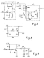
- FIG. 2 A particular embodiment of the switch 5 and of the horizontal scanning circuit is illustrated in FIG. 2.
- This switch 5 comprises two transistors 10 and 11.
- Transistor 10 receives the output voltage from gate 4 (signal S4) via a divider bridge 12 and 13.
- This transistor 10 is an NPN transistor mounted as a common emitter, its collector is connected to the base of the transistor 11 via a resistor 14 and its emitter is connected to ground.
- the transistor 11 is a PNP transistor mounted as a common emitter. The emitter of this transistor receives the supply voltage + VA, which is used to power the scanning circuit 2 and this emitter is also connected to the base of the transistor 11 via one. resistance 15.
- the collector of the transistor is connected to the chemical capacitor 8.
- transistor 10 When the voltage applied to the base of transistor 10 is positive, the base-emitter junction of this transistor is forward biased, transistor 10 conducts.
- the base-emitter junction of transistor 11 is then forward biased, the transistor conducts.
- the collector voltage of transistor 11 is substantially equal to the supply voltage + VA, the switch 5 is closed, the scanning circuit 2 is supplied.
- the scanning circuit 2 includes a THT transformer 17 supplied via the capacitor 8, the collector of the control transistor is charged by this transformer.
- This LC circuit includes a capacitor 20 in parallel on the diode 18. 11 also includes a capacitor 21 in series with a coil 19, connected in parallel on the capacitor 20. The coil 19 delivering a sawtooth current causes the deflection horizontal of the spot on the screen.
- FIG. 3 illustrates a particular embodiment of the threshold detector 3.
- This circuit includes a PNP transistor 27 mounted as a common emitter, the emitter is supplied by the signal S2, that is to say by the supply voltage of the central unit 1.
- the collector of the transistor 27 delivers the signal S3 and is connected to ground via a resistor 28.
- the base is connected to the cathode of a Zener diode 29 via a resistor 26.
- the anode of diode 29 is connected to the ground, the cathode is connected to signal S2 by a resistor 25.
- the base voltage of transistor 27 is substantially equal to the Zener voltage, as long as the voltage S2 is below the predetermined threshold, the base emitter junction is reverse biased, the transistor is blocked, the output S3 is zero.
- the voltage S2 is greater than the threshold, the emitter base junction is forward biased, the transistor 27 is saturated, the output S3 is substantially equal to S2, S3 is in the logic state "1".
- FIG. 4 illustrates a particular embodiment of the shaping circuit 7.
- This circuit includes an NPN transistor mounted as a common emitter.
- the base receives the signal H via a resistor 30.
- This resistor 30 is connected to the power supply + VA by a resistor 31.
- the collector of transistor 32 is connected to the power supply + VA by a resistor 33.
- the emitter of the transistor is connected to ground.
- a resistor 35 in series with a diode 36 are connected between the collector of transistor 32 and ground.
- the cathode of diode 36 is connected to resistor 35 while the anode is connected to ground.
- a link capacitor 34 connects the collector of transistor 32 to resistor 35.
- the transistor 32 is conducting, when the signal H has a pulse of determined and positive length, the output voltage VBE taken between the terminal A and the ground is negative.
- FIG. 5 illustrates a diagram of the signal times S4, H, the voltage of the base-emitter junction VBE of the scanning control transistor 6, the collector current lc of this transistor, and the collector voltage of this transistor 6.
- the time interval T-to corresponds to correct operation of the central unit 1, its supply voltage being correct (stable), it generates a periodic synchronization signal H whose pulse level is well determined.
- the output signal S4 of the gate 4 is in the logic state "1" during this same time interval and this corresponding to the closing of the switch 5 and therefore to the supply of the scanning circuit 2.
- the voltage VBE is negative during the pulses of the clock H, and positive when the signal H is zero.
- the transistor 6 conducts when the voltage VBE is positive, that is to say when the signal H is zero.
- the signal S4 is in logic state "0" which corresponds to the opening of the switch 5.
- the scanning circuit is no longer supplied by the supply voltage + VA. As this is a case of switching off the supply after correct operation, the scanning circuit 2 and the shaping circuit 7 are supplied by the capacitor 8 for a time determined by its time constant discharge.
- Transistor 6 is an NPN transistor of type BU806 or equivalent.
- the transistor 10 is an NPN transistor of the MPSA42 type or equivalent.
- the transistor 27 is a PNP transistor of the 2N2907 A type or equivalent.
- the transistor 32 is an NPN transistor of the BC372 type or equivalent.
- Diode 36 is of type 1 N4148 or equivalent.
Landscapes
- Engineering & Computer Science (AREA)
- Multimedia (AREA)
- Signal Processing (AREA)
- Details Of Television Scanning (AREA)
Applications Claiming Priority (2)
| Application Number | Priority Date | Filing Date | Title |
|---|---|---|---|
| FR8205243A FR2524185A1 (fr) | 1982-03-26 | 1982-03-26 | Dispositif de protection de la commande de balayage horizontal d'un ecran de visualisation |
| FR8205243 | 1982-03-26 |
Publications (2)
| Publication Number | Publication Date |
|---|---|
| EP0091333A1 EP0091333A1 (fr) | 1983-10-12 |
| EP0091333B1 true EP0091333B1 (fr) | 1986-04-30 |
Family
ID=9272451
Family Applications (1)
| Application Number | Title | Priority Date | Filing Date |
|---|---|---|---|
| EP83400535A Expired EP0091333B1 (fr) | 1982-03-26 | 1983-03-15 | Dispositif de protection de la commande de balayage horizontal d'un écran de visualisation |
Country Status (4)
| Country | Link |
|---|---|
| US (1) | US4484112A (show.php) |
| EP (1) | EP0091333B1 (show.php) |
| DE (1) | DE3363252D1 (show.php) |
| FR (1) | FR2524185A1 (show.php) |
Families Citing this family (1)
| Publication number | Priority date | Publication date | Assignee | Title |
|---|---|---|---|---|
| DE3705615A1 (de) * | 1987-02-21 | 1988-09-01 | Thomson Brandt Gmbh | Zeilenablenkschaltung fuer verschiedene zeilenfrequenzen |
Family Cites Families (4)
| Publication number | Priority date | Publication date | Assignee | Title |
|---|---|---|---|---|
| DE2057907A1 (de) * | 1970-11-25 | 1972-06-08 | Licentia Gmbh | Schutzschaltung fuer ein Geraet der Nachrichtentechnik,insbesondere einen Fernsehempfaenger |
| DE2116167C3 (de) * | 1971-04-02 | 1982-05-27 | Blaupunkt-Werke Gmbh, 3200 Hildesheim | Niederspannungs-Versorgungsschaltung für ein Fernsehempfangsgerät |
| DE2530350C3 (de) * | 1975-07-08 | 1978-10-26 | Standard Elektrik Lorenz Ag, 7000 Stuttgart | Speiseschaltung für Fernsehgeräte |
| US4162434A (en) * | 1977-11-07 | 1979-07-24 | Rca Corporation | Regulator with short circuit protection |
-
1982
- 1982-03-26 FR FR8205243A patent/FR2524185A1/fr active Granted
-
1983
- 1983-03-15 DE DE8383400535T patent/DE3363252D1/de not_active Expired
- 1983-03-15 EP EP83400535A patent/EP0091333B1/fr not_active Expired
- 1983-03-22 US US06/477,731 patent/US4484112A/en not_active Expired - Fee Related
Also Published As
| Publication number | Publication date |
|---|---|
| EP0091333A1 (fr) | 1983-10-12 |
| FR2524185A1 (fr) | 1983-09-30 |
| DE3363252D1 (en) | 1986-06-05 |
| US4484112A (en) | 1984-11-20 |
| FR2524185B1 (show.php) | 1984-05-04 |
Similar Documents
| Publication | Publication Date | Title |
|---|---|---|
| EP0537084B1 (fr) | Disjoncteur à verrouillage sélectif | |
| EP0258091B1 (fr) | Déclencheur statique numérique auto-surveille | |
| EP0002983A1 (fr) | Circuit de commande de puissance et alimentation à découpage l'utilisant | |
| CH669057A5 (fr) | Installation de surveillance et d'alarme. | |
| FR2596927A1 (fr) | Circuit de protection d'alimentation a decoupage | |
| US3378775A (en) | Method and apparatus for controlling a television receiver | |
| EP0091333B1 (fr) | Dispositif de protection de la commande de balayage horizontal d'un écran de visualisation | |
| FR2525386A1 (fr) | Dispositif de commutation de charges electriques du type resistif et selfique alimentees en courant alternatif | |
| FR2515867A1 (fr) | Dispositif a contacteurs de commande de circuits electriques | |
| EP0536058B2 (fr) | Déclencheur électronique comportant des moyens de signalisation locale du type de défaut détecté | |
| FR2618968A1 (fr) | Appareil a tuner autoprogrammable | |
| EP0789486B1 (fr) | Appareil d'affichage d'images, muni d'un dispositif de mise en veille progressif | |
| EP0891597B1 (fr) | Objet electronique portatif pour l'echange d'informations a distance | |
| EP0418168B1 (fr) | Dispositif de surveillance à distance de l'alimentation en courant d'un appareil électrique | |
| EP0536011B1 (fr) | Dispositif de commande et de protection de sorties, notamment pour automate programmable | |
| FR2577706A1 (fr) | Agencement de circuits pour un recepteur de telecommande centralisee | |
| FR2517150A1 (fr) | Circuit telephonique gere par microprocesseur a circuit integre de transmission 2 fils-4 fils et alimentation de sauvegarde par courant de ligne | |
| CH623276A5 (show.php) | ||
| KR890002390B1 (ko) | 시력보호를 위한 텔레비젼 근접 시청 방지장치 | |
| FR2733865A1 (fr) | Procede de controle d'un etage final de puissance et montage pour la mise en oeuvre de ce procede | |
| FR2680595A1 (fr) | Dispositif de controle de segment pour afficheur a cristaux liquides, et procede de controle correspondant. | |
| FR2498807A1 (fr) | Relais monostable a faible consommation | |
| US7030908B2 (en) | Method and circuit for spot-killer control in cathode-ray tube | |
| JPS6256715B2 (show.php) | ||
| EP1492392B1 (fr) | Appareil de variation de la puissance moyenne d'alimentation d'une charge en courant alternatif |
Legal Events
| Date | Code | Title | Description |
|---|---|---|---|
| PUAI | Public reference made under article 153(3) epc to a published international application that has entered the european phase |
Free format text: ORIGINAL CODE: 0009012 |
|
| AK | Designated contracting states |
Designated state(s): DE GB IT SE |
|
| 17P | Request for examination filed |
Effective date: 19840216 |
|
| GRAA | (expected) grant |
Free format text: ORIGINAL CODE: 0009210 |
|
| AK | Designated contracting states |
Kind code of ref document: B1 Designated state(s): DE GB IT SE |
|
| PG25 | Lapsed in a contracting state [announced via postgrant information from national office to epo] |
Ref country code: SE Effective date: 19860430 Ref country code: IT Free format text: LAPSE BECAUSE OF FAILURE TO SUBMIT A TRANSLATION OF THE DESCRIPTION OR TO PAY THE FEE WITHIN THE PRESCRIBED TIME-LIMIT;WARNING: LAPSES OF ITALIAN PATENTS WITH EFFECTIVE DATE BEFORE 2007 MAY HAVE OCCURRED AT ANY TIME BEFORE 2007. THE CORRECT EFFECTIVE DATE MAY BE DIFFERENT FROM THE ONE RECORDED. Effective date: 19860430 |
|
| REF | Corresponds to: |
Ref document number: 3363252 Country of ref document: DE Date of ref document: 19860605 |
|
| PLBE | No opposition filed within time limit |
Free format text: ORIGINAL CODE: 0009261 |
|
| STAA | Information on the status of an ep patent application or granted ep patent |
Free format text: STATUS: NO OPPOSITION FILED WITHIN TIME LIMIT |
|
| PGFP | Annual fee paid to national office [announced via postgrant information from national office to epo] |
Ref country code: DE Payment date: 19920218 Year of fee payment: 10 |
|
| 26N | No opposition filed | ||
| PGFP | Annual fee paid to national office [announced via postgrant information from national office to epo] |
Ref country code: GB Payment date: 19920226 Year of fee payment: 10 |
|
| PG25 | Lapsed in a contracting state [announced via postgrant information from national office to epo] |
Ref country code: GB Effective date: 19930315 |
|
| GBPC | Gb: european patent ceased through non-payment of renewal fee |
Effective date: 19930315 |
|
| PG25 | Lapsed in a contracting state [announced via postgrant information from national office to epo] |
Ref country code: DE Effective date: 19931201 |