EP0086333B1 - Digitalschaltung - Google Patents
Digitalschaltung Download PDFInfo
- Publication number
- EP0086333B1 EP0086333B1 EP83100237A EP83100237A EP0086333B1 EP 0086333 B1 EP0086333 B1 EP 0086333B1 EP 83100237 A EP83100237 A EP 83100237A EP 83100237 A EP83100237 A EP 83100237A EP 0086333 B1 EP0086333 B1 EP 0086333B1
- Authority
- EP
- European Patent Office
- Prior art keywords
- level
- potential
- signal
- transistor
- node
- Prior art date
- Legal status (The legal status is an assumption and is not a legal conclusion. Google has not performed a legal analysis and makes no representation as to the accuracy of the status listed.)
- Expired
Links
- 230000008859 change Effects 0.000 claims description 15
- 230000005669 field effect Effects 0.000 claims description 9
- 230000004044 response Effects 0.000 claims description 8
- 238000009877 rendering Methods 0.000 claims 3
- 238000010586 diagram Methods 0.000 description 5
- 230000002035 prolonged effect Effects 0.000 description 3
- 239000000654 additive Substances 0.000 description 2
- 230000000996 additive effect Effects 0.000 description 2
- 238000000034 method Methods 0.000 description 2
- 230000008901 benefit Effects 0.000 description 1
- 238000010276 construction Methods 0.000 description 1
- 230000003247 decreasing effect Effects 0.000 description 1
- 230000006870 function Effects 0.000 description 1
- 230000007257 malfunction Effects 0.000 description 1
- 230000009467 reduction Effects 0.000 description 1
Images
Classifications
-
- H—ELECTRICITY
- H03—ELECTRONIC CIRCUITRY
- H03K—PULSE TECHNIQUE
- H03K19/00—Logic circuits, i.e. having at least two inputs acting on one output; Inverting circuits
- H03K19/003—Modifications for increasing the reliability for protection
- H03K19/00346—Modifications for eliminating interference or parasitic voltages or currents
- H03K19/00361—Modifications for eliminating interference or parasitic voltages or currents in field effect transistor circuits
-
- G—PHYSICS
- G11—INFORMATION STORAGE
- G11C—STATIC STORES
- G11C7/00—Arrangements for writing information into, or reading information out from, a digital store
- G11C7/12—Bit line control circuits, e.g. drivers, boosters, pull-up circuits, pull-down circuits, precharging circuits, equalising circuits, for bit lines
Definitions
- the present invention relates to a digital circuit, and more particularly to a precharge circuit for a digital circuit employing field-effect transistors.
- Digital circuits widely adopt the precharge technique in which predetermined circuit nodes are all charged to a predetermined potential and subsequently charges accumulated at the selected circuit nodes are discharged to determine logic levels, because such precharge technic is advantageous in view of low power consumption and a high speed operation.
- a precharge control signal is commonly applied to the precharge transistors and used to control them.
- the precharge control signal is usually generated as an output signal of an inverter which receives a basic control signal such as a chip enable signal and with a predetermined slope it changes from one of binary logic levels which makes the precharge transistors non-conducting to the other of the binary logic levels which makes the precharge transistors conducting.
- a potential at gates of the precharge transistors similarly changes and the precharge transistors become conducting to feed circuit nodes such as digit lines with currents. While, a potential at the circuit nodes to be charged is gradually raised as time elapses. This raise of potential at the circuit nodes functions to reduce a gate-source voltage bias of the precharge transistors. Therefore, amount of currents fed through the precharge transistors is increased in accordance with shift in potential of the precharge control signal towards the other of the binary logic levels till a predetermined time point, and then it is decreased in accordance with the potential raise at the circuit nodes to be charged. Accordingly, the amount of currents fed throughout the precharge inevitably takes a peak value. In general, if a current having a large peak values flows in a circuit, then various harmful noises are generated thereby and in the worst case malfunction of the circuit would be caused.
- the circuit node is effectively charged already during the time when the first signal has its first and second rates of change.
- the second rate of change which is smaller than the first rate is effective for suppressing a peak value of the charging current.
- the circuit node is further charged during the time when the first signal has its third rate of change, this makes only a small contribution to the charging of the circuit node because the circuit node had already been charged to a level rather close to the final level during the time of the second rate of change of the first signal.
- the effective conductance of the precharged transistor is limited to a relatively low value and hence the peak value of the charging current fed through the precharge transistor is also limited to a small value.
- a wave form of the precharge current is made moderate throughout the precharge operation without prolonging a period of time of the precharge operation.
- CMOS structure in which N-channel field effect transistors and P-channel field effect transistors are included is employed by way of example and the logic "1" or high level corresponds to a power supply voltage (Vcc) while the logic "0" or low level corresponds to the ground potential.
- Vcc power supply voltage
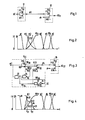
- a precharge signal generator portion 11 for generating a precharge control signal ⁇ 3 and a portion 12 forming a precharge is illustrated.
- P-channel transistors P 11 and P 12 , and N-channel transistors N 11 and N 12 are employed, and a node NO" is precharged.
- the precharge signal generator portion 11 is constructed of CMOS inverter circuit consisting of the transistors P 11 and N 11 .
- the node NO 11 to be charged is brought to a charged level, i.e., "1"-level.
- the precharge control signal ⁇ 3 becomes “1"-level, hence the transistor P 12 is turned OFF.
- the first control signal ⁇ 1 becomes "1"-level, the node NO 11 to be charged is turned to "0"-level through the transistor N 12 .
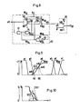
- a precharge circuit is basically composed of a precharge signal generator portion 30 for generating a precharge control signal ⁇ 4 and a precharge portion 35 responsive to the precharge control signal ⁇ 4 for charging a node N0 37 .
- the precharge portion 35 includes a P-channel transistor P 32 as a precharge transistor coupled between the node N0 37 and a power supply terminal V cc and an N-channel transistor N 35 coupled between the node N0 37 and the ground potential.
- a circuit structure of the precharge portion 35 is basically the same as the portion 12 of Fig. 1.
- the transistor P 32 charges the node N0 37 in response to "0" or low level of the precharge control signal ⁇ 4 .
- the N-channel transistor N 35 discharges the charge at the node N0 37 in response to "1" or high level of a first control signal ⁇ 1 .
- the precharge control signal generator portion 30 receives a second control signal ⁇ 2 as a basic signal for controlling precharge operation and generates the precharge control signal ⁇ 4 .
- the precharge control signal generator portion 30 includes a P-channel transistor P 31 coupled between the power supply terminal (V cc ) and an output node N0 30 and having a gate receiving the signal ⁇ 2 N-channel transistors N 31 and N 32 connected in series between the output node N0 30 and the ground potential, N-channel transistors N 33 and N 34 connected in series between the output node N0 30 and the ground potential. Gates of the transistors N 3 , and N 33 receive the signal ⁇ 2 .
- delay circuits 31 and 32, a NAND gate 34 and an inverter 33 are provided.
- the delay circuit 31 receives the signal ⁇ 2 and an output signal of the delay circuit 31 is applied to a gate of the transistor N 34 , a first input terminal of the NAND gate 34, and an input terminal of the delay circuit 32.
- An output of the delay circuit 32 is led to a second input terminal of the NAND gate 34 through the inverter 33.
- An output signal of the NAND gate 34 is applied to a gate of the transistor N 3 2.
- an effective conductance of the series circuit of the transistors N 3 , and N 32 is set far larger than that of the series circuit of the transistors N 33 and N 34 .
- the conductance of the transistors N 32 and N 34 are made substantially the same, the conductance of the transistor N 31 is made larger than that of the transistor N 33 .
- the transistor N 35 When the first control signal ⁇ 1 is at "1"-level, the transistor N 35 is turned ON and brings the node N0 37 to be charged to "0"-level i.e., discharged. Subsequently the first control signal ⁇ 1 becomes "0"-level and the transistor N 35 is turned OFF. In this instance, the signal ⁇ 2 is at "0" level, and the output signal at a node N0 34 of the delay circuit 31 is still at “0" level, and therefore the output signal at a node N0 32 of the gate 34 is at "1" level. Therefore, the transistor N 32 is conducting.
- the transistor P 31 is turned OFF and the transistor N 31 and N 33 is turned ON, so that the precharge control signal ⁇ 4 begins to fall in potential from "1"-level (V cc potential) with a large gradient m 31 that is determined by the serial ON resistances of the transistors N 3 , and N 32 .
- the transistor P 32 is turned ON to start charging of the node N0 37 to be charged.
- the conductance of the transistor P 32 rises, and hence, the charging current I cc3 for the node N0 37 to be charged is gradually increased.
- the node N0 34 is brought to "1"-Ievel via the delay circuit 31, and hence the transistor N 34 is turned ON.
- the node N0 32 is brought to "0"-level through the NAND circuit 34 because the node N0 34 is at "1" level and the node N0 35 is still at "0" level by a delay time of the delay circuit 32 to set the node N0 36 at "1" level.
- the transistor N 32 is turned OFF.
- the current path which causes potential drop of the precharge signal ⁇ 4 is switched from the transistors N 3 , and N 32 to the transistors N 33 and N 34 .
- the precharge control signal ⁇ 4 present a moderate slope indicated by m 32 that is determined by the ON resistances of the transistors N 33 and N 34 . Consequently, the rise of the conductance of the transistor P 32 also becomes moderate or suppressed. Therefore, the charging current I cc3 becomes nearly constant.
- the node N0 35 becomes "1"-level via the delay circuit 32 after a delay time of the delay circuit 32, and the node N0 36 becomes “0"-level via the inverter circuit 33.
- the node N0 32 again becomes “1"-level via the NAND circuit 34, and consequently, the transistor N 32 is turned ON.
- the potential drop of the precharge control signal ⁇ 4 again takes a steep slope indicated by m 33 towards OV. Therefore, the conductance of the transistor P 32 again starts quickrise, but at the moment t 32 in Fig.
- the potential at the node N0 37 to be charged has already come close to the V cc potential (for instance 80% or higher of the V cc potential), and hence the value of the charging current I cc3 begins to reduce.
- the transistor P 3 is turned ON, the transistors N 3 , and N 33 are turned OFF, hence the precharge control signal ⁇ 4 takes "1" level, and the transistor P 32 is turned OFF.
- the first control signal ⁇ 1 takes "1" level to bring the node N0 37 to be charged to "0"-level.
- a memory cell MC is arrayed at an intersection of a word line WL and a pair of digit lines DL and DL .
- the pair of digit lines DL and DC are precharged by P-channel transistors P 51 , P 52 and P 53 in response to "0"- level of the precharge control signal ⁇ 4 .
- the threshold voltage of the transistors P 5 , to P 53 is represented by V T p.
- the precharge control signal ⁇ 4 is at a "1"-leveI, and hence the transistors P 51 to P 53 are in an OFF state.
- one (DL) of the digit lines is at "0" level.
- the precharge control signal ⁇ 4 begins to fall in potential, and if the potential becomes a potential equal to or lower than V cc ⁇
- the potential of the precharge control signal ⁇ 4 falls, the conductances of the transistors P 51 to P 53 are increased, and hence the value of the charging current I cc5 for the digit line DL becomes large gradually.
- the slope of the precharge control signal ⁇ 4 becomes moderate the rise of the conductances of the transistors P 5 , to P 53 becomes moderate.
- the charging current I cc5 becomes nearly constant.
- the slope of the precharge control signal ⁇ 4 again becomes steep, then the conductances of the transistors P 51 to P 53 begin to rise and the digit line rises towards the V cc potential, but the charging current is reduced.
- the large peak current appearing as a charging current for digit lines is one of the important points which becomes a problem upon design of a memory circuit and also upon designing a system employing the memory circuit. More particularly, although a capacitance of a digit line in a memory circuit is a small value (for instance 1 pF) with respect to a single digit line only, as a memory capacity becomes large-sized, the number of the digit lines is increased, and the total capacitance for the entire digit lines becomes a large value. For instance, in a memory circuit of 16 K bits, the number of the digit lines is sometimes 128, and hence the peak current value produced upon charging these digit lines amounted in the prior art as large as 150 mA.
- FIG. 3 shows a detailed example of the embodiment of Fig. 3.
- the logic blocks in the above-described first preferred embodiment are replaced by transistors of CMOS constructions. Accordingly, the operation is similar to the case of the above-described first preferred embodiment. Hence, only the correspondance betwen Figs. 3 and 7 will be explained here.
- P-channel transistors P 72 to P 76 and N-channel transistors N 75 to N 79 are employed.
- the transistors P 72 , N 75 , P 73 and N 76 and the additive capacitance C 71 form a CMOS delay circuit 31 which corresponds to the delay circuit indicated with the same reference number in Fig. 3.
- the transistors P 76 and N 79 and the additive capacitance C 72 form a CMOS delay circuit and an inverter circuit in combination 32 and 33 which corresponds to the delay circuit 32 and the inverter circuit 33 in Fig. 3.
- the transistors P 74 , P 75 , N 77 and N 78 form a CMOS NAND circuit 34 which corresponds to the NAND circuit 34 with the same reference number in Fig. 3.
- a precharge control signal generator portion 80 receives a second control signal ⁇ 5 and generates a precharge control signals ⁇ 6 to be applied to a precharge transistor.
- a precharge portion 85 includes an N-channel transistor N 82 coupled between the power supply terminal (V cc ) and a node NO 87 to be precharged and an N-channel transistor N 83 coupled between the node NO 87 and the ground potential.
- the transistor N 82 charges the node NO 87 in response to a "1" level of the precharge control signal ⁇ 6 while the transistor N 83 discharges the node NO 87 in response to a "1"-level of the first control signal ⁇ 1 .
- the precharge control signal generator portion 80 includes a series circuit of P-channel transistors P 81 and P 82 and a series circuit of P-channel transistors P 83 and P 84 both connected in series between the power supply terminal (V cc ) and an output node NO so , and an N-channel transistor N 81 , coupled between the node NO 80 and the ground potential.
- Delay circuits 81 and 82, an inverter 83 and a NOR gate 84 are provided for controlling the transistors P 82 and P 84 .
- the transistor N 81 is turned OFF, while the transistors P 81 and P 83 are turned ON, so that the precharge signal ⁇ 6 rises in potential at a slope m 81 that is determined by ON resistances of the respective transistors P 81 and P 82 starting from "0"-level.
- the transistor N 82 is turned ON to start charging of the node NO 87 to be charged, and since the conductance of the transistor N 82 becomes large, the charging current I cc8 for the node NO 87 to be charged would be increased gradually.
- the second control signal ⁇ 5 becomes "0"-level
- the node N0 84 is brought to "0"-level through the delay circuit 81
- the transistor P 84 is turned ON
- the node NO 82 is brought to "1"-level via the NOR circuit 84
- the transistor P 82 is turned OFF.
- t 81 the path of the current for potential rise of the precharge signal ⁇ 6 is switched from the transistors P 81 and P 82 to the transistors P 83 and P 84 .
- the precharge signal ⁇ 6 can take a moderate slope as indicated by m 82 which is determined by the ON resistances of the respective transistors P 83 and P 84 . Consequently, the rise of the conductance of the transistor N 82 also becomes moderate, and so the charging current I cc8 becomes nearly constant.
- the node NO 85 is brought to the "0"-level via the delay circuit 82, the node N0 86 is brought to "1 "-level via the inverter circuit 83, the node NO 82 is again brought to "0"-level via the NOR circuit 84 and the transistor P 82 is turned ON. (The moment when the transistor P 82 is turned on is indicated by t 82 ). As a result, the precharge control signal ⁇ 6 again takes a steep slope as indicated by m 83 and increases towards the V cc potential.
- the conductance of the transistor 82 again makes abrupt rise.
- the potential of the node NO 87 to be charged is close to the finally reaching potential (for instance, assuming that the threshold voltage of the transistor N 82 is 0.8 V, a potential equal to or higher than 80% of V cc ⁇ 0.8 V)
- the potential at the node NO 87 to be charged will be finally reaching potential while the value of the charging current I cc8 is being reduced.
- the second control signal ⁇ 5 becomes "1"-level
- the transistors P 81 and P 83 are turned OFF, the transistor N 81 is turned ON and the precharge control signal ⁇ 6 becomes "0"- level.
- the first control signal ⁇ 1 becomes "1"-level, so that the node NO 87 to be charged becomes "0"-level.
- Fig. 10 are illustrated waveforms of the precharge signals and the charging current in the prior art and according to the present invention, respectively.
- a waveform 3 is the precharge signal in the prior art shown in Fig. 1 and a waveform 4 shows a precharge sig signal according to the present invention.
- I cc1 designates a waveform I cc1 shows a charging current for a node to be charged in the prior art, while a waveform I cc3 shows a charging current for a node to be charged according to the present invention. If potential fall arises just as the precharge control signal 3 in the prior art, then the conductance of the transistor P 12 shown in Fig.
- the waveform of the charging current I cc3 for the node N0 37 to be charged takes a shape of a trapezoid, and as compared to the wave form of an accute-angled isosceles triangle of the charging current I cc1 , the peak value can be reduced (for example up to 60% of the prior art) without extending the charging time, that is, while the area of the figure surrounded by the waveform and the time axis (corresponding to the total charging quantity) is maintained the same as shown in Fig. 10.
- a peak current upon operation of the parts is large, it would become a source of harmful noises, and therefore, reduction of a peak current is very effective.
Landscapes
- Physics & Mathematics (AREA)
- Engineering & Computer Science (AREA)
- Computer Hardware Design (AREA)
- Computing Systems (AREA)
- General Engineering & Computer Science (AREA)
- Mathematical Physics (AREA)
- Logic Circuits (AREA)
- Read Only Memory (AREA)
- Dram (AREA)
- Static Random-Access Memory (AREA)
Claims (3)
Applications Claiming Priority (2)
| Application Number | Priority Date | Filing Date | Title |
|---|---|---|---|
| JP57003787A JPS58121195A (ja) | 1982-01-13 | 1982-01-13 | プリチヤ−ジ信号発生回路 |
| JP3787/82 | 1982-01-13 |
Publications (2)
| Publication Number | Publication Date |
|---|---|
| EP0086333A1 EP0086333A1 (de) | 1983-08-24 |
| EP0086333B1 true EP0086333B1 (de) | 1986-06-25 |
Family
ID=11566887
Family Applications (1)
| Application Number | Title | Priority Date | Filing Date |
|---|---|---|---|
| EP83100237A Expired EP0086333B1 (de) | 1982-01-13 | 1983-01-13 | Digitalschaltung |
Country Status (4)
| Country | Link |
|---|---|
| US (1) | US4570083A (de) |
| EP (1) | EP0086333B1 (de) |
| JP (1) | JPS58121195A (de) |
| DE (1) | DE3364218D1 (de) |
Families Citing this family (10)
| Publication number | Priority date | Publication date | Assignee | Title |
|---|---|---|---|---|
| JPS60182096A (ja) * | 1984-02-29 | 1985-09-17 | Fujitsu Ltd | 半導体記憶装置 |
| JPS6194290A (ja) * | 1984-10-15 | 1986-05-13 | Fujitsu Ltd | 半導体メモリ |
| US4751680A (en) * | 1986-03-03 | 1988-06-14 | Motorola, Inc. | Bit line equalization in a memory |
| US4779010A (en) * | 1986-07-29 | 1988-10-18 | Advanced Micro Devices, Inc. | Monostable logic gate in a programmable logic array |
| US4751407A (en) * | 1986-12-19 | 1988-06-14 | Hughes Aircraft Company | Self-timing circuit |
| US4857764A (en) * | 1988-06-30 | 1989-08-15 | Harris Corporation | Current compensated precharged bus |
| DE69232170T2 (de) * | 1992-06-26 | 2002-06-06 | Stmicroelectronics S.R.L., Agrate Brianza | Puffer mit niedrigem Rauschen |
| US5748022A (en) * | 1995-10-31 | 1998-05-05 | Texas Instruments Incorporated | Input circuit |
| DE19836736C1 (de) * | 1998-08-13 | 1999-12-30 | Siemens Ag | Kombinierte Vorlade- und Homogenisierschaltung |
| US6480419B2 (en) | 2001-02-22 | 2002-11-12 | Samsung Electronics Co., Ltd. | Bit line setup and discharge circuit for programming non-volatile memory |
Citations (3)
| Publication number | Priority date | Publication date | Assignee | Title |
|---|---|---|---|---|
| EP0027905A1 (de) * | 1979-09-28 | 1981-05-06 | Nec Corporation | Schaltung zur Erzeugung eines verzögerten Signales |
| EP0030813A2 (de) * | 1979-12-05 | 1981-06-24 | Fujitsu Limited | Spannungserhöhungsschaltungen |
| EP0032017A1 (de) * | 1979-12-19 | 1981-07-15 | Fujitsu Limited | Bootstrapschaltung |
Family Cites Families (9)
| Publication number | Priority date | Publication date | Assignee | Title |
|---|---|---|---|---|
| JPS52146274A (en) * | 1976-05-31 | 1977-12-05 | Toshiba Corp | Output circuit |
| US4123799A (en) * | 1977-09-19 | 1978-10-31 | Motorola, Inc. | High speed IFGET sense amplifier/latch |
| US4208730A (en) * | 1978-08-07 | 1980-06-17 | Rca Corporation | Precharge circuit for memory array |
| DE2904674C2 (de) * | 1979-02-08 | 1980-11-20 | Standard Elektrik Lorenz Ag, 7000 Stuttgart | Schaltungsanordnung mit einem als Schalter dienenden Transistor |
| US4222112A (en) * | 1979-02-09 | 1980-09-09 | Bell Telephone Laboratories, Incorporated | Dynamic RAM organization for reducing peak current |
| JPS5730192A (en) * | 1980-07-29 | 1982-02-18 | Fujitsu Ltd | Sense amplifying circuit |
| US4458336A (en) * | 1980-10-22 | 1984-07-03 | Fujitsu Limited | Semiconductor memory circuit |
| US4404474A (en) * | 1981-02-06 | 1983-09-13 | Rca Corporation | Active load pulse generating circuit |
| US4414480A (en) * | 1981-12-17 | 1983-11-08 | Storage Technology Partners | CMOS Circuit using transmission line interconnections |
-
1982
- 1982-01-13 JP JP57003787A patent/JPS58121195A/ja active Granted
-
1983
- 1983-01-13 DE DE8383100237T patent/DE3364218D1/de not_active Expired
- 1983-01-13 EP EP83100237A patent/EP0086333B1/de not_active Expired
- 1983-01-13 US US06/457,596 patent/US4570083A/en not_active Expired - Lifetime
Patent Citations (3)
| Publication number | Priority date | Publication date | Assignee | Title |
|---|---|---|---|---|
| EP0027905A1 (de) * | 1979-09-28 | 1981-05-06 | Nec Corporation | Schaltung zur Erzeugung eines verzögerten Signales |
| EP0030813A2 (de) * | 1979-12-05 | 1981-06-24 | Fujitsu Limited | Spannungserhöhungsschaltungen |
| EP0032017A1 (de) * | 1979-12-19 | 1981-07-15 | Fujitsu Limited | Bootstrapschaltung |
Also Published As
| Publication number | Publication date |
|---|---|
| EP0086333A1 (de) | 1983-08-24 |
| US4570083A (en) | 1986-02-11 |
| DE3364218D1 (en) | 1986-07-31 |
| JPH0222472B2 (de) | 1990-05-18 |
| JPS58121195A (ja) | 1983-07-19 |
Similar Documents
| Publication | Publication Date | Title |
|---|---|---|
| EP0205294B1 (de) | Leseverstärkungsschaltung für eine integrierte Schaltung | |
| US4574203A (en) | Clock generating circuit providing a boosted clock signal | |
| EP0072686B1 (de) | Pufferschaltung mit einer Inverterschaltung | |
| US5151614A (en) | Circuit having charge compensation and an operation method of the same | |
| US5537060A (en) | Output buffer circuit for memory device | |
| KR100419816B1 (ko) | 신호 전위 변환 회로 | |
| US4754170A (en) | Buffer circuit for minimizing noise in an integrated circuit | |
| EP0086333B1 (de) | Digitalschaltung | |
| US4833643A (en) | Associative memory cells | |
| US5073872A (en) | Data output control circuit for semiconductor storage device | |
| KR102670315B1 (ko) | 논-타겟 odt 기능을 가진 출력 버퍼 회로 | |
| US4894559A (en) | Buffer circuit operable with reduced power consumption | |
| EP0048922B1 (de) | Dynamische Signalerzeugungsschaltung | |
| US5210449A (en) | Edge triggered tri-state output buffer | |
| JPH021456B2 (de) | ||
| EP0115140B1 (de) | Dekodierschaltung | |
| US5652727A (en) | Semiconductor memory device | |
| US4447893A (en) | Semiconductor read only memory device | |
| US4467456A (en) | Memory circuit | |
| KR100301602B1 (ko) | 출력파형의링잉을억제하는것이가능한반도체장치 | |
| WO1984002042A1 (en) | Schmitt trigger circuit | |
| US4353104A (en) | Output interface circuits | |
| US5732025A (en) | Output interfacing device programmable among three states for a memory in CMOS technology | |
| US5218241A (en) | AND circuit and address circuit employing the same | |
| KR940006076B1 (ko) | 그라운드 노이즈가 감소된 데이타 출력버퍼 |
Legal Events
| Date | Code | Title | Description |
|---|---|---|---|
| PUAI | Public reference made under article 153(3) epc to a published international application that has entered the european phase |
Free format text: ORIGINAL CODE: 0009012 |
|
| PUAI | Public reference made under article 153(3) epc to a published international application that has entered the european phase |
Free format text: ORIGINAL CODE: 0009012 |
|
| AK | Designated contracting states |
Designated state(s): DE FR GB NL |
|
| RAP1 | Party data changed (applicant data changed or rights of an application transferred) |
Owner name: NEC CORPORATION |
|
| 17P | Request for examination filed |
Effective date: 19831108 |
|
| GRAA | (expected) grant |
Free format text: ORIGINAL CODE: 0009210 |
|
| AK | Designated contracting states |
Kind code of ref document: B1 Designated state(s): DE FR GB NL |
|
| REF | Corresponds to: |
Ref document number: 3364218 Country of ref document: DE Date of ref document: 19860731 |
|
| ET | Fr: translation filed | ||
| PLBE | No opposition filed within time limit |
Free format text: ORIGINAL CODE: 0009261 |
|
| STAA | Information on the status of an ep patent application or granted ep patent |
Free format text: STATUS: NO OPPOSITION FILED WITHIN TIME LIMIT |
|
| 26N | No opposition filed | ||
| PGFP | Annual fee paid to national office [announced via postgrant information from national office to epo] |
Ref country code: GB Payment date: 19920108 Year of fee payment: 10 |
|
| PGFP | Annual fee paid to national office [announced via postgrant information from national office to epo] |
Ref country code: FR Payment date: 19920109 Year of fee payment: 10 |
|
| PGFP | Annual fee paid to national office [announced via postgrant information from national office to epo] |
Ref country code: NL Payment date: 19920131 Year of fee payment: 10 |
|
| PGFP | Annual fee paid to national office [announced via postgrant information from national office to epo] |
Ref country code: DE Payment date: 19920324 Year of fee payment: 10 |
|
| PG25 | Lapsed in a contracting state [announced via postgrant information from national office to epo] |
Ref country code: GB Effective date: 19930113 |
|
| PG25 | Lapsed in a contracting state [announced via postgrant information from national office to epo] |
Ref country code: NL Effective date: 19930801 |
|
| GBPC | Gb: european patent ceased through non-payment of renewal fee |
Effective date: 19930113 |
|
| NLV4 | Nl: lapsed or anulled due to non-payment of the annual fee | ||
| PG25 | Lapsed in a contracting state [announced via postgrant information from national office to epo] |
Ref country code: FR Effective date: 19930930 |
|
| PG25 | Lapsed in a contracting state [announced via postgrant information from national office to epo] |
Ref country code: DE Effective date: 19931001 |
|
| REG | Reference to a national code |
Ref country code: FR Ref legal event code: ST |