EP0084376A2 - Knock control system - Google Patents
Knock control system Download PDFInfo
- Publication number
- EP0084376A2 EP0084376A2 EP83100396A EP83100396A EP0084376A2 EP 0084376 A2 EP0084376 A2 EP 0084376A2 EP 83100396 A EP83100396 A EP 83100396A EP 83100396 A EP83100396 A EP 83100396A EP 0084376 A2 EP0084376 A2 EP 0084376A2
- Authority
- EP
- European Patent Office
- Prior art keywords
- circuit
- resistor
- signal
- gain
- output
- Prior art date
- Legal status (The legal status is an assumption and is not a legal conclusion. Google has not performed a legal analysis and makes no representation as to the accuracy of the status listed.)
- Withdrawn
Links
Images


Classifications
-
- F—MECHANICAL ENGINEERING; LIGHTING; HEATING; WEAPONS; BLASTING
- F02—COMBUSTION ENGINES; HOT-GAS OR COMBUSTION-PRODUCT ENGINE PLANTS
- F02P—IGNITION, OTHER THAN COMPRESSION IGNITION, FOR INTERNAL-COMBUSTION ENGINES; TESTING OF IGNITION TIMING IN COMPRESSION-IGNITION ENGINES
- F02P5/00—Advancing or retarding ignition; Control therefor
- F02P5/04—Advancing or retarding ignition; Control therefor automatically, as a function of the working conditions of the engine or vehicle or of the atmospheric conditions
- F02P5/145—Advancing or retarding ignition; Control therefor automatically, as a function of the working conditions of the engine or vehicle or of the atmospheric conditions using electrical means
- F02P5/15—Digital data processing
- F02P5/152—Digital data processing dependent on pinking
- F02P5/1527—Digital data processing dependent on pinking with means allowing burning of two or more fuels, e.g. super or normal, premium or regular
-
- F—MECHANICAL ENGINEERING; LIGHTING; HEATING; WEAPONS; BLASTING
- F02—COMBUSTION ENGINES; HOT-GAS OR COMBUSTION-PRODUCT ENGINE PLANTS
- F02P—IGNITION, OTHER THAN COMPRESSION IGNITION, FOR INTERNAL-COMBUSTION ENGINES; TESTING OF IGNITION TIMING IN COMPRESSION-IGNITION ENGINES
- F02P5/00—Advancing or retarding ignition; Control therefor
- F02P5/04—Advancing or retarding ignition; Control therefor automatically, as a function of the working conditions of the engine or vehicle or of the atmospheric conditions
- F02P5/145—Advancing or retarding ignition; Control therefor automatically, as a function of the working conditions of the engine or vehicle or of the atmospheric conditions using electrical means
- F02P5/15—Digital data processing
- F02P5/152—Digital data processing dependent on pinking
- F02P5/1526—Digital data processing dependent on pinking with means for taking into account incorrect functioning of the pinking sensor or of the electrical means
-
- Y—GENERAL TAGGING OF NEW TECHNOLOGICAL DEVELOPMENTS; GENERAL TAGGING OF CROSS-SECTIONAL TECHNOLOGIES SPANNING OVER SEVERAL SECTIONS OF THE IPC; TECHNICAL SUBJECTS COVERED BY FORMER USPC CROSS-REFERENCE ART COLLECTIONS [XRACs] AND DIGESTS
- Y02—TECHNOLOGIES OR APPLICATIONS FOR MITIGATION OR ADAPTATION AGAINST CLIMATE CHANGE
- Y02T—CLIMATE CHANGE MITIGATION TECHNOLOGIES RELATED TO TRANSPORTATION
- Y02T10/00—Road transport of goods or passengers
- Y02T10/10—Internal combustion engine [ICE] based vehicles
- Y02T10/40—Engine management systems
Landscapes
- Engineering & Computer Science (AREA)
- Signal Processing (AREA)
- Chemical & Material Sciences (AREA)
- Combustion & Propulsion (AREA)
- Mechanical Engineering (AREA)
- General Engineering & Computer Science (AREA)
- Electrical Control Of Ignition Timing (AREA)
- Combined Controls Of Internal Combustion Engines (AREA)
Abstract
A gain control system comprising a gain variable amplifier (205) for amplifying an input signal linearly, a gain control circuit (206) for producing a gain control signal for controlling the gain of the amplifier on the basis of an output signal of the amplifier, and a gain control signal controller for controlling the gain control signal to prevent the gain of the gain variable amplifier from changing abruptly.
Description
- The present invention relates to a knock control system for an internal combustion engine, or more in particular to a knock control system for detecting a knock signal accurately thereby to control a knock properly regardless of engine speed.
- The knock generated in the engine is accompanied by a knocking noise and therefore reduces the running performance on one hand and a reverse torque is generated thereby to reduce the engine output or the engine overheated is destroyed on the other hand. The knock thus , generated has a close relation with the ignition timing, and it is known that the characteristics of the engine are such that the engine output is maximized by setting the ignition timing, namely, the ignition advance angle immediately before a knock. If the ignition advance is reduced to avoid the knocking, the engine output is reduced, and therefore the ignition timing is required to be controlled at a point immediately before a knocking.
- Generally, the output of a knock sensor for detecting a knock sound increases with the increase of engine speed, which in turn increases the background level (BGL), with the result that any knocking that may occur is accurately detected.
- Since the BGL is obtained by averaging the output of the knock sensor and by making use of charge and discharge of a capacitor, however, the gain of a gain variable amplifier changes with the ripple carried in the output signal of the knock sensor. Although the knock signal is capable of following the ripple change, the output signal of the averaging circuit of BGL is delayed and therefore a knock cannot be detected accurately by comparison of the two signals.
- Accordingly, it is the object of the present invention to provide a knock control system capable of accurate knock control.
- In order to achieve this object, according to the present invention, there is provided a knock control system in which the output of a gain control circuit for controlling the gain of the gain variable amplifier for amplifying the knock signal is provided with an integration time constant thereby to effect accurate knock control.
- The above and other objects, features and advantages will be made apparent by the detailed description taken in conjunction with the accompanying drawings, in which:
- Fig. 1 is a diagram showing a general configuration of a typical example of a knock control system according to the present invention;
- Figs. 2 to 8 show the circuits of various parts in detail;
- Fig. 9 is a time chart showing signal waveforms produced at the various parts of Fig. 1;
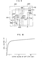
- Fig. 10 shows a BPF voltage - BG voltage characteristic; and
- Figs. 11 and 12 show the ignition timing characteristic of a knock control system according to the present invention.
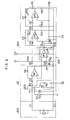
- The present invention will be explained below in detail with reference to the accompanying drawings. Fig. 1 shows a block diagram of a typical example of a knock control system according to the present invention.
- In the drawing, a knock control system comprises a
knock sensor 100 for detecting a knock signal, aknock control unit 200 for applying a control signal for controlling the ignition timing of anignition coil 600 in response to the knock signal supplied from theknock sensor 100, apickup coil 400 for detecting the spark timing of theignition coil 600, and a contactless ignition means 500 for igniting the ignition coil and supplying a feedback signal to theknock control unit 200 in response to the output of thepickup coil 400 and theknock control unit 200. - The
knock control unit 200, in response to a detection signal of theknock sensor 100 and an output signal of the contactless ignition means 500, controls the contactless ignition means 500 thereby to control the ignition advance or retardation in accordance with the knocking involved. - The
knock control unit 200 includes anamplifier 201 having an ignitionnoise cut circuit 202 with a gate for cutting off the ignition noises in synchronism with the spark timing, a band pass filter (BPF) 204 for passing the knock signal, a gain variable amplifier circuit (AGC circuit) 205 for controlling the gain of the amplifier thereof in proportion to the input signal ratio in response to the output ofBPF 204, amask circuit 207. for masking the AGC output for a predetermined timing period, a halfwave rectifier ciruit 208 for half-wave rectifying the input signal supplied from theAGC circuit 205 through themask circuit 207, a knocksignal clamp circuit 209 for preventing the background level from being affected by a large knock signal inserted in the half wave signal of the halfwave rectifier circuit 208, a background level (BGL)detector circuit 210 for obtaining the average value of the knock signals, again control circuit 206 for amplifying the output of theBGL detector circuit 210 and feeding back it to theAGC circuit 205, asignal amplifier circuit 211 for amplifying the output of themask circuit 207, acomparator 212 for comparing the output voltage of theBGL detector circuit 210 with the output signal of thesignal amplifier circuit 211 and producing a retardation signal proportional to the knocking, amask circuit 214 for masking the output of thecomparator 212 at a predetermined timing and producing an output, a knock signalvoltage converter circuit 215 for integrating the output of themask circuit 214 and producing a voltage value corresponding to the retardation signal proportional to the knocking, a fail-safe circuit 213 for detecting an open fault of theknock sensor 100 and therby retarding the ignition timing forcibly, amonostable circuit 216 for producing a signal of a predetermined pulse duration in synchronism with the cutoff of the ignition coil 600 (namely, in synchronism with the base current of the power transistor 503) in response to the signal from the contactless ignition means 500, anF-V generator 217 for producing a voltage proportional to the engine speed in response to the output pulse of themonostable circuit 216, a 2000-rpm detector circuit 218 for producing a signal associated with 2000 r.p.m. or higher engine speed in response to the output of theF-V generator 217, a 4000-rpm detector circuit 219 for producing a signal when the engine speed is 4000 r.p.m. or higher, a low-voltage detector circuit 220 for suspending the knock control by detecting a battery voltage drop at the time of engine start, and a referencevoltage generator circuit 203. - The contactless ignition means 500 includes an
amplifier 501 for shaping the waveform of the output signal of thepickup coil 400, aretard circuit 502 for controlling the ignition timing in accordance with the output voltage of theknock control circuit 200, and thepower transistor 503 for generating a high voltage on the secondary side of theignition coil 600. - Now, the circuits of the knock control means 200 will be explained in detail.
- The detailed circuits of the
knock sensor 100, theamplifier 201, the ignitionnoise cut circuit 202, the referencevoltage generator circuit 203 and the bandpass filter (BPF) 204 are shown in Fig. 2. - Specifically, the
knock sensor 100 is of capacitance type using a piezoelectric element and is equivalently a parallel circuit including a capacitor C and a constant current source. - The positive terminal (+) of the
knock sensor 100 is connected with a resistor Rl, the other end of which is connected to a resistor R2, a resistor R3, the cathode of a zener diode ZD1 and the collector of a transistor Tl. The other end of the resistor R2, the anode of the zener diode AD1, and the emitter of the transistor Tl are grounded. The base of the transistor Tl is connected to the monostable circuit (OSM) 216 through a resistor R6. The other terminal of the resistor R3 is connected to the negative terminal (-) of an operational amplifier OP1 through a capacitor C2. The operational amplifier OP1 is negatively fed back with the output thereof through a resistor R4, and the output terminal of the operational amplifier OP1 is connected with resistors R7 and R8. The other end of the resistor R7 is grounded, and the other end of the resistor R8 is connected to capacitors C4, C5 and avariable resistor 9. - The resistors Rl, R2, R3, R4, R7, the capacitor C2, and the operational amplifier OP1 make up an
amplifier circuit 201, while the transistor Tl and the resistor R6 construct the ignitionnoise cut circuit 202. - The other end of the variable resistor R9 is grounded, and the other end of the capacitor C4 is connected to the input terminal (-) of the operational amplifier OP2. The other end of the capacitor C5 is connected to the output terminal of the operational amplifier OP2. The operational amplifier OP2 is negatively fed back with the output thereof through the resistor R10. The positive input terminal (+) of the operational amplifier OP2 is connected to the output terminal of the operational amplifier OP3. The output terminal of the operational amplifier OP2 is connected to resistors Rll and R17. The other end of the resistor R17 is grounded, and the other end of the resistor Rll is connected to a variable resistor R12 and capacitors C6 and C7. The other end of the variable resistor R12 is grounded, and the other end of the capacitor C6 is connected to the negative terminal (-) of an operational amplifier OP4. The operational amplifier OP4 is fed back negatively with the output thereof through a resistor R13. The other end of the capacitor C7 is connected to the output terminal of the operational amplifier OP4. The positive input terminal (+) of the operational amplifier OP4 is connected to the output terminal of the operational amplifier OP3. The output terminal of the operational amplifier OP4 is connected through a resistor R18 to a resistor R19 of the gain
variable amplifier circuit 205. The other end of this resistor R18 is grounded. - The resistors R8, R9, R10, Rll, R12, R13, R17, R18, the capacitors C4, C5, C6, C7 and the operational amplifiers OP2, OP4 make up the bandpass filter (BPF) 204. This
BPF 204 is a two-stage filter. - The positive input terminal (+) of the operational amplifier OP3 is connected to a capacitor C14 and a variable resistor R15. The other ends of the capacitor C14 and the resistor 15 are grounded. The operational amplifier OP3 is supplied with a source voltage as a drive power through S2. The operational amplifier OP3 is negatively fed back with the output thereof and has an output terminal connected with a resistor R16 and a capacitor C19. The other ends of the resistor R16 and the capacitor C19 are grounded. The power terminal of the operational amplifier OP3 is grounded through the capacitor C3.
- The resistors R15, R16, the capacitors C3, C14, C19 and the operational amplifier OP3 make up the reference
voltage generator circuit 203. By changing the resistance values of the resistors R14 and R15, the output RV of the operational amplifier OP3 is fixed to a reference voltage of, say, 3.6 V. - Fig. 3 shows detailed circuits of the
gain variable amplifier 205, thegain control circuit 206, themask circuit 207 and the halfwave rectifier circuit 208. - In this drawing, the terminal S5 shown in Fig. 2 is connected with a resistor R19, which in turn is connected to the positive terminal (+) of an operational amplifier OP5 and a variable resistor R20. The other end of this variable resistor R20 is connected to the terminal S6 shown in Fig. 2. The negative input terminal (-) of the operational amplifier OP5 is connected to resistors R21, R22 and R23. The other end of this resistor R22 is connected to the drain of an FET. The source of this FET is connected to the terminal S6 shown in Fig. 2, and the gate thereof is connected to a resistor R30 and a capacitor C15. The other end of this capacitor C15 is grounded, and the other end of the resistor R30 is connected to the output terminal of the operational amplifier OP7. The other end of the resistor R21 is connected to the positive input terminal (+) of the operational amplifier OP7. The other end of the resistor R23 is connected to the output terminal of the operational amplifier OP5. The output terminal of the operational amplifier OP5 is connected to the resistors R24 and R110. The other end of this resistor R110 is grounded. The other end of the resistor R24 is connected to the terminal S7, the capacitor C8 and the collector of the transistor T2. The capacitor C8 is connected through a resistor R27 to the negative input terminal (-) of the operational amplifier OP6. The negative input terminal (-) of the operational amplifier OP6 is connected to a resistor R25 and the anode of a diode Dl. The cathode of this diode Dl is connected to the output terminal of an operational amplifier OP6 and the anode of a diode D2. The cathode of this diode D2 is connected to a resistor R25 and the terminal S8.
- The positive input terminal (+) of the operational amplifier OP6 is connected to the emitter of the transistor T2 and the positive input terminal (+) of an operational amplifier OP7. The base of the transistor T2 is connected through a resistor R29 to terminal S3. The negative input terminal (-) of the operational amplifier OP7 is connected to the resistor R31, a variable resistor R33, and a resistor R46. The other end of this resistor R31 is connected to the output terminal of the operational amplifier OP7, and the other end of the variable resistor R33 is grounded. The other end of the resistor R46 is connected to the terminal S9. The output terminal of the operational amplifier OP7 is grounded via a resistor R32.
- The resistors R19, R20, R21, R22, R23, the field effect transistor, and the operational amplifier OP5 make up the gain
variable amplifier circuit 205. - The resistors R30, R31, R32, R33, R46, the capacitor C15, and the operational amplifier OP7 make up the
gain control circuit 206. - 'The resistors R24, R29, R110 and the transistor T2 make up the
mask circuit 207. - Further, the resistors R25, R27, R28, the capacitor C8, the diodes Dl, D2, and the operational amplifier OP6 make up the half
wave rectifier circuit 208. - Fig. 4 shows detailed circuits of the knock
signal clamp circuit 209, the background level (BGL)detector circuit 210, thesignal amplifier circuit 211, thecomparator 212, and the fail-safe circuit 213. - In the diagram, the terminal S7 of Fig. 3 is connected through the capacitor Cl to a resistor R26. The other end of this resistor R26 is connected to a variable resistor R36 and the input terminal (-) of an operational amplifier OP8. The other end of the variable resistor R36 is connected to the output terminal of the operational amplifier OP8.
- The capacitor Cl, the resistors R26, R36 and the operational amplifier OP8 make up the
signal amplifier circuit 211. - The operational amplifier OP8 is supplied power from the terminal S2, and has a terminal grounded. The positive input terminal (+) of the operational amplifier OP8 is connected to the variable resistor R35 and the terminal 513. The other end of the variable resistor R35 is connected to the terminal Sl of Fig. 2 through a resistor R34. The other end of the variable resistor R35 is connected to the negative input terminal (-) of an operational amplifier OP9. The positive input terminal (+) of the operational amplifier OP9 is connected to the terminal S9. The output terminal of the operational amplifier OP9 is connected to a resistor R37, the other end of which is connected to a resistor R105 and the terminal S10. The other end of this resistor R105 is grounded.
- The resistors R34, R35, R37, R105 and the operational amplifier OP9 make up the fail-
safe circuit 213. - The output terminal of the operational amplifier OP8 is connected to the resistor R54 and the positive input terminals (+) of comparators C01 and C02. The other end of this resistor R54 is grounded. The terminal Sl is connected to the anode of a diode D12 through a resistor R103, and the cathode of this diode D12 is connected to the base of a transistor T3 and a resistor R104. The emitter of this transistor T3 is connected to the resistors R39 and R40, and the collector thereof is grounded. The other end of this resistor R39 is connected to the terminal S8 and the resistor R38, and the other end of the resistor R38 is grounded. The other end of the resistor R40 is connected to the positive input terminal (+) of an operational amplifier OP10 and a capacitor C16. The other end of this capacitor C16 is connected to the terminal S13. The negative input terminal (-) of the operational amplifier OP10 is connected to a resistor R43, the resistor R44 and the resistor R45. The other end of the resistor R43 is . connected to the resistor R41 and the variable resistor R42. The other end of the resistor R41 is connected to the terminal Sl. The other end of the variable resistor R42 is grounded. The other end of the resistor R44 is connected to the terminal S13. The other end of the resistor R45 is connected to the output terminal of an operational amplifier OP10. The output terminal of the operational amplifier OP10 is connected to the terminal S9 and the positive input terminal (+) of the operational amplifier OP9.
- The other end of the resistor R104, on the other hand, is connected to the terminal S13.
- The resistors R103, R104, the diode D12 and the transistor T3 make up the knock
signal clamp circuit 209. - The resistors R54, R38, R39, R40, R41, R42, R43, R44, R45, the capacitor C16, and the operational amplifier OP10 make up the background level (BGL)
detector circuit 210. - The negative input terminal (-) of the comparator C01 of which the positive input terminal (+) is connected to the output terminal of the operational amplifier OP8 is connected to the resistor R47 and the variable resistor R48. The other end of this resistor R47 is connected to the terminal Sl, and the other end of the variable resistor R48 is connected to the terminal S13. The output terminal of the operational amplifier OP8 is connected to the positive input terminal (+) of the comparator C02, of which the negative terminal (-) is connected to the output terminal of the operational amplifier OP10. The output terminal of the comparator COl is connected to the terminal Sll, and the output terminal of the comparator C02 is connected to the terminal S12.
- The resistors R47, R48, and the comparators C01, C02 make up the
comparator circuit 212. - Detailed circuits of the
mask circuit 214, and the knock signalvoltage converter circuit 215 are shown in Fig. 5. - In the drawing, the terminal S3 of Fig. 2 is connected through a resistor R51 to the base of a transistor T5, and the collector of the transistor T5 is connected to a resistor R52, while the emitter thereof is grounded.
- The resistors R51, R52 and the transistor T5 make up the
mask circuit 214. - The terminal Sll of Fig. 4 is connected to the resistors R49, R50 and the anode of the diode D3. The terminal S12 of Fig. 4 is similarly connected to the resistors R49, R50 and the anode of the diode D3. The other end of this resistor R49 is connected to the terminal Sl of Fig. 2. The other end of the resistor R50 is connected to the cathode of the diode D3. The cathode of the diode D3 is connected to the resistors R52, R53 and a capacitor C9. The other end of the capacitor C9 is grounded, and the other end of the resistor R53 is connected to the resistor R54, the collector of a transistor T6 and the base of a transistor T7. The other end of the resistor R54 is connected to the terminal S14. The collector of the transistor T7 is connected to a variable resistor R63, and the emitter thereof is grounded. The base of the transistor T6 is connected to a resistor R61, and the emitter of the transistor T6 is grounded, The other end of the resistor R61 is connected to the terminal S17 and the resistor R60. The other end of the resistor R60 is connected to the base of the transistor T4, the collector of which is connected through a resistor R62 to the terminal Sl of Fig. 2, while the emitter thereof is connected to the cathode of the diode D5 and the negative input terminal (-) of an operational amplifier OP11. The negative input terminal (-) of the operational amplifier OP11 is connected to a capacitor C17, a resistor R57 and the anode of a diode D4. The other end of the resistor R57 is connected to the resistors R55 and R56. The other end of the resistor R55 is connected to the terminal Sl of Fig. 2. The other end of the resistor R56 is connected to the terminal S4 of Fig. 2, the terminal S13 of Fig. 4, and the positive input terminal (+) of the operational amplifier OP11.
- The other end of the capacitor C17 is connected via the capacitor C18 to the output terminal of the operational amplifier OPll. The output terminal of the operational amplifier OPll is connected to a resistor R64, the positive input terminal (+) of the operational amplifier OP12, the positive input terminal (+) of the operational amplifier OP13 and the resistor R73. The other end of the resistor R64 is grounded, and the negative input terminal (-) of the operational amplifier OP12 is connected through a resistor R69 to the terminal Sl of Fig. 2. The output terminal of the operational amplifier OP12 is connected through a resistor R65 to the anode of a diode D5 and a capacitor C10. The other end of the capacitor C10 is grounded. The negative input terminal (-) of the operational amplifier OP12 is connected to resistors R70 and R71. The other end of the resistor R70 is grounded. The other end of the resistor R71 is connected to the terminal S16 and the collector of a transistor T8. The emitter of the transistor T8 is grounded, and the base thereof is connected via a resistor R72 to the terminal S14.
- On the other hand, the negative input terminal (-) of the operational amplifier OP13 is connected through the resistor R67 to the resistor R68 and the terminal S15. Also, the output terminal of the operational amplifier OP13 is connected to the cathode of the diode D4.
- The resistor R73 is connected to the capacitor Cll and the signal terminal SIG. The other end of the capacitor Cll is grounded.
- The knock signal
voltage converter circuit 215 is comprised of the resistors R49, R50, R53, R54, R55, R56, R57, R60, R61, R62, R63, R64, R65, R66, R67, R68, R69, R70, R71, R72, R73, the capacitors C9, C10, Cll, C17, C18, the diodes D3, D4, D5, the transistors T4, T6, T7, T8, the operational amplifier OPll, OP12, OP13. - Fig. 6 shows the monostable multivibrator circuit (OSM) 216 in detail.
- In the diagram, the input terminal IG supplied with the ignition signal, namely, the signal from the
power transistor 503 is connected to a resistor R74, the other end of which is connected to a capacitor C12, the cathode of a diode D6 and the base of a transistor T9. The other end of this capacitor C12 and the anode of the diode D6 are grounded. The emitter of the transistor T9 is grounded, and the collector thereof is connected to a resistor R75 and a resistor R76. The other end of the resistor R75 is connected to the terminal Sl of Fig. 2, and the other end of the resistor R76 is connected to the base of a transistor T10 and a resistor R81. The emitter of the transistor T10 is grounded, and the collector thereof is connected to the cathode of a diode D8. The anode of the diode D8 is connected to resistors R78 and R79. The other end of the resistor R78 is connected to the terminal Sl of Fig. 2, and the other end of the resistor R79 is connected through a capacitor C13 to the base of a transistor Tll. The base of the transistor Tll is also connected to the terminal Sl of Fig. 2 through a resistor R80, and the emitter thereof is connected to the earth. The collector of the transistor Tll is connected to a resistor R81, a resistor R82 and the terminal S3 of Fig. 2. The other end of the resistor R82 is connected to the terminal S2 of Fig. 2. - The resistors R74, R75, R76, R78, R79, R80, R81, the capacitors C12, C13, the diodes D6, D8, and the transistors T9, T10, Tll make up a
monostable multivibrator circuit 216. - Fig. 7 shows the
F-V generator circuit 217, the 2000-rpm detector circuit 218, and the 4000-rpm detector circuit 219 in detail. - In Fig. 7, the terminal S15 of Fig. 5 is connected to the positive input terminal (+) of an operational amplifier OP14. The negative input terminal (-) of this operational amplifier OP14 is connected to a resistor R85, a variable resistor R84 and a capacitor C19. The other end of the resistor R85 is connected to the output terminal of the operational amplifier OP14. The other end of the variable resistor R84, on the other hand, is connected to the collector of a transistor T12. The emitter of the transistor T12 is grounded, and the base thereof is connected to the terminal S3 of Fig. 2 through a resistor R83. The other end of the capacitor C19 is connected to the output terminal of the operational amplifier OP14. The output terminal of this operational amplifier OP14 is connected through a resistor R86 to a resistor R87, the negative input terminal (-) of a comparator C03 and the negative input terminal (-) of a comparator C04. The operational amplifier OP14 is supplied with a power source from the terminal S2 of Fig. 2, and has a terminal grounded. The positive input terminal (+) of the comparator C03 is connected to resistors R88, R89, and the anode of a diode D9, and the other end of the resistor R89 is grounded. The other end of the resistor R88 is connected to the terminal Sl of Fig. 2. The cathode of the diode D9 is connected via a resistor R90 to the output terminal of the comparator C03. The output terminal of the comparator C03 is connected to resistors R91 and R92. The other end of the resistor R91 is connected to the terminal S2 of Fig. 2, the other end of the resistor R92 being connected to the terminal S10 of Fig. 4 and the base of a transistor T13. The emitter of the transistor T13 is grounded, and the collector thereof is connected to the terminal S14 of Fig. 5 and a resistor R93. The other end of the resistor R93 is connected to the terminal S2 of Fig. 2.
- On the other hand, the positive input terminal (+) of the comparator C04 is connected to resistors R94 and R95. The other end of the resistor R94 is connected to the terminal S2 of Fig. 2, and other end of the resistor R95 is connected to a resistor R109 and the anode of a diode D10. The other end of the resistor R109 is grounded. The cathode of the diode D10 is connected to the output terminal of the comparator C04 through a resistor R96. The comparator C04 is supplied with power from the terminal S2 of Fig. 2, and is grounded. The output terminal of the comparator C04 is connected to the terminal S16 shown in Fig. 5.
- The resistors R83, R84, R85, R86, the transistors T12, the capacitor C19, and the operational amplifier OP14 make up the
F-V generator 217. - The resistors R87, R88, R89, R90, R91, the diode D9, and the comparator C03 make up the 2000-
rpm detector circuit 218. - Furhter, the resistors R92, R93, R94, R95, R96, R109, the transistor T13, the diode D10 and the comparator C04 make up the 4000-
rpm detector circuit 219. - The diagram of Fig. 8.illustrates the low-
voltage detector circuit 220, and thesource voltage circuit 300 in detail. - In the drawing, the terminal S17 of Fig. 5 is connected to a resistor R97, the collector of a transistor T14 and a capacitor C23. The other end of the resistor R97 is connected to the battery power supply V+. Also, the emitter of the transistor T14 is grounded, and the base thereof is connected to the other end of the capacitor C23, the resistor R93, the cathode of the diode Dll and the anode of the zener diode ZD3. The other end of the resistor R98 is grounded and the anode of the diode Dll is also grounded. The cathode of the zener diode ZD3 is connected to the battery V+ through the resistor R99. The cathode of the zener diode ZD3 is connected to the resistor R100 and the capacitor C20. The other end of the resistor R100 and the other end of the capacitor C20 are both grounded.
- The resistors R97, R98, R99, the capacitors C20, C23, the diode Dll, the zener diode ZD3 and the transistor T14 make up the low-
voltage detector circuit 220. - The battery power supply V+ is connected through the resistor R101 to the terminal S2 of Fig. 2. The resistor R101 is connected to the cathode of the zener diode ZD4 and the capacitor C21. The anode of this zener diode ZD4 and the other end of the capacitor C21 are both grounded.
- On the other hand, the battery power supply V+ is connected to the resistor R102, and the other end of this resistor R102 is connected to' the terminal Sl of Fig. 2, the cathode of the zener diode ZD5 and the capacitor C22. The anode of the zener diode ZD5 and the other end of the capacitor C22 are both grounded.
- The resistors R101, R102, the capacitors C21, C22 and the zener diodes ZD4, ZD5 make up the
source voltage circuit 300. - Now, the operation of the
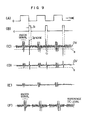
knock control system 200 will be explained. - First, the signal as shown in Fig. 9 (A) is applied to the terminal IG of Fig. 6, whereupon the transistor T9 is turned on at the "high" state of this signal, and the transistor T10 is turned off. When the transistor T10 is turned off, the route of current flow from the terminal Sl of the power supply, through the resistor R78, the resistor R79, the capacitor C13, to the transistor Tll is formed. On the other hand, the "low" state of the base signal turns off the transistor T9, while the transistor T10 is turned on, so that the route of current flow from the terminal Sl of the power supply through the resistor R80, the capacitor C13, the resistor R79, the diode D8, the transistor T10 to the ground is formed. These two routes provide a charge-discharge circuit for the capacitor C13, so that the a pulse in synchronism with the spark timing with the time duration of tl as shown in Fig. 9 (B) is generated at the collector terminal of the transistor Tll. This signal is applied to the base of the transistor Tl of the ignition noise cut
circuit 202 thereby to provide an ignition noise cut signal. At the same time, this signal is applied to the base of the transistor T2 of themask circuit 207. Further, the same signal is applied to the base of the transistor T5 of themask circuit 214 to function as an ignition noise cut signal. Fig. 9 (A) shows an ignition timing waveform, which actually provides the base signal of thepower transistor 503 of the contactless ignition means 500 described later. At "high" state of this signal, thepower transistor 503 is turned on, while at "low" level thereof, thepower transistor 503 is turned off. The spark of the ignition coil is generated in the course of switching from "on" to "off" of the transistor. The signal of Fig. 9 (B) provides a pulse output signal of a predetermined duration of themonostable multivibrator circuit 216 for generating a pulse signal of predetermined duration of t1 by being triggered at the time of switch from "on" to "off" of the base signal. In other words, this signal provides the collector waveform of the transistor Tll. - If the input impedance of the knock control system is increased, the external noises are likely to be superimposed. A typical external noise is the ignition noise (Ig noise) generated in synchronism with the ignition timing.
- The ignition noise of this system will be explained below. The base control of the
power transistor 503 is effected by the pulse as shown in Fig. 9 (A). At "high" state of this pulse, thepower transistor 503 is turned on, and vice versa. In the course of switching from "on" to "off" state of this transistor, or when thetransistor 503 is turned off, the secondary voltage of the ignition coil sharply increases, thus generating the primary noises. Further, with the increase of the secondary voltage, the insulation of the air layer between the plugs is broken for ignition. At the time of ignition, the secondary noise is generated. The secondary noise is classified into the noise caused by the capacitance discharge current flowing in the initial state of ignition and the noise caused by the induction discharge current flowing in subsequent stage. Among the secondary noises, the former makes up a larger noise source. When the input impedance is increased, the primary noise and the secondary noise (former noise) are superimposed on the output of the knock sensor as an external noise adversely affecting the knock signal discrimination. - This external noise is required to be removed. This external noise persists for the priod of about 50 to 60 µsec. During this period, the knock sensor should be masked. For this purpose, the ignition noise cut
circuit 207 is provided. The actual masking period is set to, say, about 0.8 msec sufficiently longer than the noise period mentioned above. - When the signal as shown in Fig. 9 (C) is produced from the
knock sensor 100, the amplitude of the signal is reduced by being divided by the resistors Rl and R2 as shown in Fig. 9 (D) and the reduced signal is applied to the ignition noise cutcircuit 202. The signal thus detected by theknock sensor 100 is one pulsating between positive and negative with the DC zero level as a reference. This ignition noise cutcircuit 202 functions mainly by the transistor Tl. The transistor Tl is turned on and off by the output of themonostable multivibrator circuit 216. Themonostable circuit 216 generates a pulse of the masking period by being triggered at the fall of the base signal of thepower transistor 503 shown in Fig. 9 (A). The output of themonostable circuit 216 is shown in Fig. 9 (B) and has the time of t1 making up the masking period. The transistor Tl is turned on only during the period t1 when the output of themonostable multivibrator circuit 216 is "1". As a result, during the period tl, the output of the knock sensor is shorted to the earth, so that the input to the operational amplifier OPl is eliminated thereby to mask the ignition noises. - The signal as shown in Fig. 9 (E) is produced from the ignition noise cut
circuit 202. - The signal shown in Fig. 9 (E) is amplified at the operational amplifier OP1 on the one hand and the signal shown in Fig. 9 (F) is produced from the output terminal of the operational amplifier OP1 as a signal (3.6 V) of DC level by the feedback of the signal of the reference
voltage generator circuit 203 on the other hand. The amplification factor (G) of this operational amplifier OP1 is given as G =
- The signal shown in Fig. 9 (F) is applied to the bandpass filter (BPF) 204. The
bandpass filter 204 emphasizes and produces the knock signal (attenuating the other signals) and has a characteristic of attenuating the other signals at a frequency slightly higher than the knock signal. The gainvariable amplifier circuit 205, in response to the feedback signal from the backgroundlevel detector circuit 210 through thehalfwave rectifier circuit 208, changes the gain thereof in inverse proportion to the BGL output, namely, the feedback signal. Themask circuit 207 masks the output of the gainvariable amplifier circuit 205 at a predetermined timing. This masking operation is performed by the pulse signal of Fig. 9 (B). In response to the output of themask circuit 205, theBGL detector circuit 210 detects the background level. Thecomparator 212 compares the BGL output (voltage) of theBGL detector circuit 210 with the output of thesignal amplifier circuit 211. The output signal as shown in Fig. 9 (G) is produced at the output terminal of the operational amplifier OP4 of thebandpass filter 204. The signal shown in Fig. 9 (G) is applied to the gainvariable amplifier circuit 205. - One feature of the system under consideration is the circuit configuration between the gain
variable amplifier circuit 205 and thecomparator circuit 212. The outputs S5 and S6 of thebandpass filter 204 are applied to the gainvariable amplifier circuit 205. The output of the gainvariable amplifier circuit 205 is divided into two routes through themask circuit 207. The first route is for amplifying the knock signal by theamplifier 211 and applying the amplified signal to one of the input terminals of thecomparator circuit 212. The second route is includes thehalfwave rectifier circuit 208, the knocksignal clamp circuit 209, and theBGL detector circuit 210 having an integrator circuit and an amplifier circuit. The outpt of theBGL detector circuit 210 is applied to the other input terminal of thecomparator circuit 212. The output of theBGL detector circuit 212 is negatively fed back to the gainvariable amplifier circuit 205 through thegain control circuit 206. - The output of the
knock sensor 100 ranges from ±5 mV to ±600 mV. Specifically, the sensor output varies in the range up to 120 times. If this output is simply amplified, say, by 100 times, the voltage of ±0.5 V to ±60 V is obtained. In the case of an automobile, the maximum battery voltage is about 12 V, and the voltage of 60 V is not used. Conventionally, therefore, a small gain is used to avoid saturation or the output is processed taking the saturation for granted. The former method results in a low sensitivity against a minute output, while the latter method leads to a low sensitivity against an input of large amplitude. The configuration of the embodiment under consideration is characterized by the provision of gainvariable amplifier circuit 205 and that this gainvariable amplifier circut 205 is inserted on the output side of thebandpass filter 204 thereby to give an integration time constant to the output of thegain control circuit 206. By this configuration, the level difference between the knock signal and a non-knock signal is increased and an input is applied to the gainvariable amplifier circuit 205 with this increased level difference, with the result that even at the time of a sudden change of the background level, the signal and the background level can be changed at the same rate, thus producing an output of superior S/N ratio. - The output filtered through the
bandpass filter 204 is thus applied through the resistor R19 to the operational amplifier OP5 of the gainvariable amplifier circuit 205. The negative terminal of the operational amplifier OP5 is provided with an FET the gain of which is controlled through thegain control circuit 206. As a result, the gain of the gainvariable amplifier circuit 205 is changed in accordance with the output of the operation amplifier OP10. The output of the gainvariable amplifier circuit 205 is masked at a predetermined timing by themask circuit 207, and through the capacitor C18 and the resistor R21 applied to the halfwave rectifier circuit 208. - The gain G (Z) of the gain
variable amplifier circuit 205 is given as described below. - Let the output resistance of the field effect transistor in the non-saturated region be r. Then r is expressed as

- The gain G(Z) of the gain
variable amplifier circuit 205 is given as
bandpass filter 204 is about several mV. As a result, the value of VDS in equation (2) is sufficiently small as compared with the voltage VGS, so that in this calculation the value VDS of equation (2) is handled as 0 V. - The waveform produced from the gain
variable amplifier circuit 205, which carries the ignition noise mentioned above, is masked by themask circuit 207. Specifically, the trasistor T2 of themask circuit 207 is turned on by the output signal of themonostable multivibrator circuit 216 applied to the base of the transistor T2. The turning on of the transistor T2 causes the output of the gainvariable amplifier circuit 205 to drop to the earth potential and is masked. - The signal thus masked is applied to the half-
wave rectifier circuit 208 and thesignal amplifier circuit 211. - In the half-
wave rectifier circuit 208, the diodes Dl and D2 function to rectify only the positive half component of the signal and the resulting signal is applied to the knocksignal clamp circuit 209. The knock signal is further integrated and smoothed by an integrator circuit including the resistor R40 and the capacitor C16 of the backgroundlevel detector circuit 210 and after being amplified at the operational amplifier OP10, is applied to thecomparator circuit 212. - The
signal amplifier circuit 211, on the other hand, has an amplification function at the amplification factor of the operational amplifier OP8. - The gain Gl of the half
wave rectifier circuit 208 is given as

- Assuming that the half wave peak voltage is E, the gain G2 of the integrator including the resistor R40 and the capacitor C16 at the time of application of the half wave rectification signal is given as

- As a result, the terminal voltage VC(t) of the capacitor C16 is


- On the other hand, let the difference of BGL with the voltage Vref (the output voltage of the reference
voltage generator circuit 203 of, say, 3.6 V) be ΔVBGL, the output voltage of the gain control circuit be VC, and the output voltage of thebandpass filter 204 be Vin . Then from equations (2), (3), (4) and (9), the background level voltage is given as
- The gate-source voltage (VGS) of the field effect transistor is given as


- In this way, the characteristics as shown in Fig. 10 are obtained from the calculation formula with VP = about 2 V, R0 = 85 Ω and YO = about 12 mΩ for the field effect transistor.
- The background level thus obtained and the signal are compared with each other at the
comparator 212 as shown in Fig. 9 (H). - The relation between the gain
variable amplifier circuit 205 providing the feature of the embodiment under consideration and thegain control circuit 206 will be described below. - The gain
variable amplifier circuit 205 is controlled by the output produced at the output terminal of the output operational amplifier OP7 of thegain control circuit 206. When the output of the operational amplifier OP7 is "high", the gate voltage of the field effect transistor is increased and the non-saturation resistance (drain-source resistance of about 200 Ω) of the field effect transistor is small. Thus the gain of the operational amplifier OP5 is greatly increased (by about 30 times). On the other hand, if the output of the operational amplifier OP7 is small, the gate voltage of the field effect transistor is decreased so that the non-saturation resistance between drain and source is very large (say, about 20 KΩ) while the gain of theoperational amplifier OP5 is very small (say, three times). - If the background level voltage is higher than, say, 3.6 V at the division point of the resistors R46 and R33, for instance, the gain of the operational amplifier OP5 is decreased. When the background voltage is lower than 3.6 V, by contrast, the gain of the operational amplifier OP5 is increased.
- An integrator circuit comprised of the
resistor R30 and the capacitor C15 is provided at the output side of thegain control circuit 206. This integrator circuit has a time constant of about 0.5 seconds larger than that of the integrator circuit (about 0.2 seconds or smaller) comprised of the capacitor C16 and the resistor R40 of the backgroundlevel detector circuit 210. As a result, the gain is maintained substantially constant during the period of about 0.5 seconds. - Engine vibrations undergo constant changes even when the revolutional speed and the load conditions are constant. Such vibrations always contain small ripples. Without the integrator circuit including the resistor R30 and the capacitor C15, therefore, the gain (of the gain variable amplifier circuit 205) is suddenly changed against the vibration ripple signal. Although the output signal of the sensor changes following the sudden change of the gain, the background level to be compared with the knock sensor output signal at the
comparator 212 is delayed in response by the time constant on account of the integration time constant (of about 0.2 seconds) due to the resistor R40 and the capacitor C16. Then the previous background level instead of the background level associated with the knocking is undesirably compared. - The
comparator 212 produces a rectangular wave as shown in Fig. 9 (I). This pulse signal is applied to the knock signalvoltage converter circuit 215 through themask circuit 214. - In the
mask circuit 214, the transistor T5 is turned on by the output signal from themonostable multivibrator circuit 216, when the output of thecomparator 212 flows to the earth and is masked through the transistor T5. When the transistor T5 is off, the output signal from thecomparator 212 is stored in the capacitor C9 and through the resistor R53, drives the transistor T7. The transistor T7 is driven by the output signal of the 4000-rpm detector circuit 219 through the resistor R54. The source voltage applied to the base of thetransistor T6 from the terminal S17 is the output voltage of the low-voltage detector circuit 220. At the time of engine start, the battery voltage is lower than a predetermined lowest allowable voltage. This is also the case when the battery capacity is decreased. At the time of this abnormal voltage drop, a high voltage is applied to the base of the transistor T6, while a low voltage is applied thereto at the time of high voltage. When this voltage is high, the transistor T6 is turned on, and the transistor T7 is kept off regardless of the signal applied through the resistors R53 and R54. When the voltage applied to the base of the transistor T6 is low, on the other hand, the transistor T6 is turned off, with the result that the transistor T7 is turned on and off by the voltage value through the resistors R53 and R54. - In Fig. 5, the resistors R55, R56, R57, R60, R62 and the transistor T4 make up a fixed advance angle setting circuit. The advance output signal thus produced is determined by the source voltage supplied from the terminal S17 for the advance at the time of engine start.
- The operational amplifier OP11, the capacitors C17, C18 and the resistor R64 make up an integrator. The operational amplifier OP12, the resistors R65, R69, R70, R71, R73, R72, the diode D5, and the transistor T8 make up a maximum voltage clamp circuit. Further, the operational amplifier OP13, the resistors R67, R68 and the diode D4 make up a minimum voltage clamp circuit. The integrator, the maximum voltage clamp circuit and the minimum voltage clamp circuit provide an integrator circuit.
- Assume that the knock signal produced from the
comparator 212 turns on the transistor T7 in synchronism with the knock signal. As shwon in Fig. 9 (I), during the pulse duration of t0 (about 40 to 70 psec) of the knock signal, the transistor T7 conducts and the current i1 flows from the operational amplifier OP11 through the capacitors C18, C17, the resistor R63 and the transistor T7 to the earth. At this time, the operational amplifier OP11 produces an output voltage of 3.6 V. - Under this condition, the voltage increase rate AV1 of the operational amplifier OP11 for each pulse (voltage increase per pulse) is given from


- The zener voltage of the zener diode ZD4 is 6 V. The voltage at the positive terminal (+) of the operational amplifier OP11 stands at 3.6 V.
- The current i2 is expressed as


- The integrator circuit is adapted to provide a specified advance characteristic (advance value) by the turning on of the transistor T4 in response to the output voltage of the low-
voltage detector circuit 220 at the time of engine start. This advance characteristic is such that the actual advance (retard) is controlled by theretard circuit 502 in accordance with the command of the integrator circuit of the knock signalvoltage converter circuit 215. Thisretard circuit 502 is provided, for instance, by the circuit disclosed in the U.S. Patent Application Serial No. 80202, by Noboru Sugiura, filed October 1, 1979 and assigned to the assignee of this application "Ignition Timing Control System for Internal Combustion Engine". - The operation of the
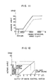
retard circuit 502 will be described below. - Generally, the ignition timing characteristic is relative and is determined by the distributor and an operating mode which is in turn determined by the ignition system used. The maximum retard characteristic is prepared for the knocking, and this characteristic is followed at the time of a knocking. Fig. 11 shows the advance and retard characteristics, in which the solid line represents the minimum retard characteristic (minimum clamp voltage) for a certain operating mode and the dotted line represents the maximum retard (maximum clamp voltage) at the time of a knocking. At the time of a low speed below, say, 200 r.p.m, the control is effected to attain the maximum advance characteristic depending on the ignition timing characteristic as far as possible. The use of this characteristic is in order to accomplish the starting without fail. If the ignition timing is delayed at the time of engine start, the engine is subjected to reverse torque so that a very large load is imposed on the starter. As a result, the drive current for the starter is abnormally increased to such a degree that the engine cannot be started by the starter, thereby leading to a starting failure. In order to prevent such a starting failure, the maximum advance characteristic determined by the ignition timing characteristic is attained at the speed of 200 r.p.m. or lower at the time of starting.
- The retard circuit for attaining the above- mentioned feature is shown in Fig. 12. As shown in the drawing, the retard characteristic inclined by a predetermined angle is provided against the output voltage of the integrator, namely, the output of the knock signal
voltage converter circuit 215. Consequently, an advance of a predetermined angle is secured for each period. In other words, the ignition timing is advanced by a predetermined angle for each period while being retarded in accordance with the number of the knocking pulses. - The battery source is connected to the V+ terminal, and being cut at a level higher than a predetermined voltage (6.2 V) by the zener diode ZD5, produces B = 6.2 V. A voltage reflecting the start detection is produced at the terminals S2 and S17. Specifically, the battery voltage is decreased at the time of engine start. When this decrease exceeds a reference value, the transistor T14 is turned off to give the same value for the terminals S2 and S17. The same operation is performed when the power capacity of the battery is decreased. When the source voltage of the battery is normal, the transistor T14 is turned on and the terminal S17 is substantially reduced to the earth potential, the voltage at the terminal S2 being equivalent to the voltage drop due to the resistor R97. The resistor R97 is set to a comparatively high level of 22 KQ. This voltage of the terminal S17 is applied to the base of the transistor T4 and the base of the transistor T6 to set a predetermined advance characteristic for engine start.
- Now, the operation of the integrator circuit for controlling the
retard circuit 502, specifically, the advancing operation at the time of engine start will be described. The zener diode ZD3 has a zener voltage of about 6 V. When the source voltage V+ is low, that is, at the time of engine start with the starter on, the voltage at the middle point of the resistors R99 and R100 is incapable of turning on the zener diode ZD3. As a result, the transistor T14 is turned off and the transistors T6 and T7 are turned on. Under this condition, the transistor T7 is turned off. With the transistor T4 turned on, the current flows in the same direction as the current i2 through the resistor R62 from the power supply, so that the output of the operational amplifier OP11 is reduced to the same voltage as the voltage at point k and clamped. The voltage at point k corresponds to the minimum clamp voltage of 1.5 V shown in Fig. 12. The output thus clamped sets the maximum retard characteristic for engine start shown by the dotted line in Fig. 11. As a result, the retard circuit 132 is controlled and thereby set to the maximum retard characteristic. - Now, the
F-V generator 217 will be explained. The transistor T12 is turned on when two conditions are met, that is, when the output signal of themonostable multivibrator circuit 216 is in "high" state and the transistor T9 is off. The transistor T12 is thus turned on for the pulse duration of t1 shown in Fig. 9 (B). The period of this pulse is proportional to the engine speed and therefore the transistor T12 is turned on in accordance with the engine speed. The positive terminal of the operational amplifier OP14 is impressed with the voltage of about 1.7 V at the junction point of the resistors R67 and R68. When the transistor T12 is on, the route is formed from the output side of the operational amplifier OP14 to the capacitor C19 to the resistor R84 to the transistor T12 to the earth thereby to charge the capacitor C19. When the transistor T12 is off, the charges of the capacitor C19 flow into the resistor R85. The operational amplifier OP14 produces an output corresponding to the error between the voltages applied to the negative and positive terminals thereof, which output voltage is applied to the negative terminal of the comparator C03. The positive terminal of the comparator C03 is supplied with a constant voltage of 3.0 V divided by the resistors R88 and R89. The negative terminal of the comparator C03, on the other hand, is supplied with a voltage corresponding to the engine speed higher than 1.7 V which is compared with the constant voltage of 3 V. When the voltage thus compared is 3 V or higher, the output of the comparator C03 is reduced to "low" state, while when it is lower than 3 V, the output is raised to "high" state. The reference voltage of 3 V is corresponds to high engine speed. Specifically, the engine speed corresponding to this voltage of 3 V is set to 2000 r.p.m. Only when the engine speed is lower than 2000 r.p.m., therefore, the output of the comparator C03 is raised to "high" state. When the engine speed is lower than 2000 r.p.m., the transistor T8 of the knock signalvoltage converter circuit 215 is turned on. With the turning on of the transistor T8, the voltage applied to the negative terminal of the operational amplifier OP12 is reduced below the voltage associated with the turning off of the transistor T8. The diode D9 and the resistor R90 are required to be provided with the hysteresis and take time before responding to the engine speed of 2000 r.p.m. During this period, the engine speed may increase to some degree, so that the output is produced taking this increase into account. - The output of the operational amplifier OP14 is applied to the negative terminal (-) of the comparator C04. The positive terminal (+) of this comparator circuit C04 is impressed with a constant voltage of 5.0 V divided by the resistors R94, R95 and R109 connected in series. The negative terminal (-) of the comparator C04 is supplied with the voltage higher than 1.7 V corresponding to the engine speed, which voltage is compared with the constant voltage of 5 V. When the voltage thus compared is higher than 5 V, the output of the comparator C04 is reduced to "low" state, while if it is lower than 5 V, the output of the comparator C04 is raised to "high" state. The voltage of 5 V providing a reference is one corresponding to the high engine speed. Specifically, the engine speed corresponding to this 5 V is set to 4000 r.p.m. Consequently, the output of the comparator C04 is raised to "high" only when the engine speed of lower than 4000 r.p.m. is involved. When the engine speed exceeds 4000 r.p.m., the voltage applied to the negative terminal (-) of the operational amplifier OP12 is reduced as if the transistor T8 of the knock signal
voltage converter circuit 215 is turned on. - Now, the fail-
safe circuit 218 will be described. This fail-safe circuit 218 is for open detection and decides at the operational amplifier OP9 whether or not the background voltage is higher than 1 V in a certain engine speed range higher than 2000 r.p.m. The voltage at the negative terminal (-) of this operational amplifier OP9 stands at a reference voltage Vref of 3.6 V plus 1 V. Under normal conditions, the background voltage is higher than 1 V for more than 2000 r.p.m. An input open condition, under which the background voltage is lower than 1 V, can be detected. - In normal operation, the positive input (+) of the operational amplifier OP9 is higher and therefore a "high" signal is produced from the output thereof, which signal is applied to the base of the transistor T13 thereby to turn on the same transistor. With the transistor T13 turned on, the normal knock control is effected since the transistor T8 of the knock signal
voltage converter circuit 215 is cut off. In the case where an open fault is involved, however, the transistor T13 is turned off and the transistor T8 is turned on, so that the timing is retarded to the maximum retard value. - According to the embodiment under consideration, therefore, the sensor output signal and the background level may be compared with each other as a value amplified at the same gain.
- It will thus be understood from the foregoing description that according to the present invention, the knock control is effected accurately.
Claims (5)
1. A gain control system comprising:
a gain variable amplifier (205) for amplifying an input signal linearly;
a gain control circuit (206) for producing a gain control signal for controlling the gain of said amplifier on the basis of an output signal of said amplifier; and
means (R30, C15) for controlling said gain control signal to prevent the gain of said gain variable amplifier from changing abruptly.
2. A gain control system according to Claim 1, wherein averaging means (208, 209, 210) is interposed between said gain variable amplifier and said gain control circuit for averaging the output signal of said gain variable amplifier and applying the resulting signal to said gain control circuit.
3. A gain control system according to Claim 2, wherein the time constant of said control means is larger than the time constant of said averaging means.
4. A knock control system comprising:
an amplifier (201) for amplifying a signal from a knock sensor for detecting the engine vibrations and producing the same;
bandpass filter (204) for producing a knocking frequency region of the output of said amplifier;
a gain variable amplifier circuit (205) for variably amplifying the output of said bandpass filter;
first means (208, 209, 210) for halfwave rectifying and averaging the output signal of said gain variable amplifier circuit;
a knock signal amplifier circuit (211) for amplifying by a predetermined amount the signal produced from said gain variable amplifier circuit;
a gain control circuit (206) for producing a control signal for controlling the gain of said gain variable amplifier circuit in response to the output of said first means;
comparator means (212) for comparing the output value of said first means with the output value of said knock signal amplifier circuit;
knock control means (215) for producing a signal for retarding the ignition timing in accordance with the knock intensity in response to the result of comparison of said comparator means; and
time constant means (R30, C15) for providing a time constant to the control signal applied to said gain variable amplifier circuit from said gain control circuit.
5. A knock control system according to Claim 1, wherein the time constant of said time constant means is larger than the integration time constant of said first means.
Applications Claiming Priority (2)
| Application Number | Priority Date | Filing Date | Title |
|---|---|---|---|
| JP57007091A JPS58124067A (en) | 1982-01-19 | 1982-01-19 | Knocking control device |
| JP7091/82 | 1982-01-19 |
Publications (2)
| Publication Number | Publication Date |
|---|---|
| EP0084376A2 true EP0084376A2 (en) | 1983-07-27 |
| EP0084376A3 EP0084376A3 (en) | 1984-10-03 |
Family
ID=11656404
Family Applications (1)
| Application Number | Title | Priority Date | Filing Date |
|---|---|---|---|
| EP83100396A Withdrawn EP0084376A3 (en) | 1982-01-19 | 1983-01-18 | Knock control system |
Country Status (3)
| Country | Link |
|---|---|
| US (1) | US4528955A (en) |
| EP (1) | EP0084376A3 (en) |
| JP (1) | JPS58124067A (en) |
Cited By (2)
| Publication number | Priority date | Publication date | Assignee | Title |
|---|---|---|---|---|
| EP0269426A1 (en) * | 1986-11-27 | 1988-06-01 | LUCAS INDUSTRIES public limited company | Knock detection system |
| EP0424917A2 (en) * | 1989-10-24 | 1991-05-02 | Japan Electronic Control Systems Co., Ltd. | System for identifying misfire cylinder in internal combustion engine |
Families Citing this family (13)
| Publication number | Priority date | Publication date | Assignee | Title |
|---|---|---|---|---|
| JPH0756334B2 (en) * | 1985-12-10 | 1995-06-14 | マツダ株式会社 | Automatic transmission control device |
| US4667637A (en) * | 1986-01-08 | 1987-05-26 | Brunswick Corporation | Gated knock detector for internal-combustion engines |
| US4644918A (en) * | 1986-04-14 | 1987-02-24 | General Motors Corporation | Knock control with AGC having reduced knock dependence |
| US4664083A (en) * | 1986-04-14 | 1987-05-12 | General Motors Corporation | Adaptive knock control with variable knock tuning |
| US4763625A (en) * | 1987-06-09 | 1988-08-16 | Brunswick Corporation | Cold start fuel enrichment circuit |
| US4761992A (en) * | 1987-06-09 | 1988-08-09 | Brunswick Corporation | Knock detection circuit with gated automatic gain control |
| US4777913A (en) * | 1987-06-09 | 1988-10-18 | Brunswick Corporation | Auxiliary fuel supply system |
| JPH01150053A (en) * | 1987-12-07 | 1989-06-13 | Nissan Motor Co Ltd | Control device for engine with automatic transmission |
| KR940004351B1 (en) * | 1990-09-27 | 1994-05-23 | 미쓰비시덴키가부시키가이샤 | Knock detector |
| WO1998031928A1 (en) * | 1997-01-20 | 1998-07-23 | Yanmar Diesel Engine Co., Ltd. | Method of knocking control of internal combustion engine |
| US20090078027A1 (en) * | 2007-09-25 | 2009-03-26 | Lycoming Engines, A Division Of Avco Corporation | Aircraft engine cylinder assembly knock detection and suppression system |
| JP5963474B2 (en) | 2012-02-29 | 2016-08-03 | キヤノン株式会社 | Information processing apparatus, information processing method, and program |
| JP6001334B2 (en) * | 2012-05-31 | 2016-10-05 | ルネサスエレクトロニクス株式会社 | Semiconductor device, battery state monitoring module, and vehicle system |
Citations (5)
| Publication number | Priority date | Publication date | Assignee | Title |
|---|---|---|---|---|
| FR2274796A1 (en) * | 1974-06-12 | 1976-01-09 | Raffinage Cie Francaise | Engine ignition timing system based on pinking - sensitive detector on engine supplying actual pinking detector |
| FR2398895A1 (en) * | 1977-07-26 | 1979-02-23 | Exxon Research Engineering Co | METHOD AND APPARATUS FOR AUTOMATIC CONTROL OF THE IGNITION POINT OF AN INTERNAL COMBUSTION ENGINE |
| JPS55114878A (en) * | 1979-02-28 | 1980-09-04 | Nippon Denso Co Ltd | Ignition timing controller of internal combustion engine |
| FR2449798A1 (en) * | 1979-02-23 | 1980-09-19 | Sev Marchal | ELECTRONIC DEVICE FOR DETECTING CLICK IN THE OPERATION OF AN INTERNAL COMBUSTION ENGINE |
| GB2066894A (en) * | 1979-12-04 | 1981-07-15 | Nissan Motor | Knocking detector for an internal combustion engine |
Family Cites Families (4)
| Publication number | Priority date | Publication date | Assignee | Title |
|---|---|---|---|---|
| US4116175A (en) * | 1976-07-28 | 1978-09-26 | General Motors Corporation | Internal combustion engine ignition spark timing system modulated by cylinder combustion pressure |
| GB2061380B (en) * | 1979-10-11 | 1983-11-02 | Nissan Motor | Knocking detector for controlling ignition timing of an internal combustion engine |
| JPS5726673U (en) * | 1980-07-22 | 1982-02-12 | ||
| JPS5738667A (en) * | 1980-08-14 | 1982-03-03 | Hitachi Ltd | Knock controller |
-
1982
- 1982-01-19 JP JP57007091A patent/JPS58124067A/en active Granted
-
1983
- 1983-01-17 US US06/458,324 patent/US4528955A/en not_active Expired - Fee Related
- 1983-01-18 EP EP83100396A patent/EP0084376A3/en not_active Withdrawn
Patent Citations (5)
| Publication number | Priority date | Publication date | Assignee | Title |
|---|---|---|---|---|
| FR2274796A1 (en) * | 1974-06-12 | 1976-01-09 | Raffinage Cie Francaise | Engine ignition timing system based on pinking - sensitive detector on engine supplying actual pinking detector |
| FR2398895A1 (en) * | 1977-07-26 | 1979-02-23 | Exxon Research Engineering Co | METHOD AND APPARATUS FOR AUTOMATIC CONTROL OF THE IGNITION POINT OF AN INTERNAL COMBUSTION ENGINE |
| FR2449798A1 (en) * | 1979-02-23 | 1980-09-19 | Sev Marchal | ELECTRONIC DEVICE FOR DETECTING CLICK IN THE OPERATION OF AN INTERNAL COMBUSTION ENGINE |
| JPS55114878A (en) * | 1979-02-28 | 1980-09-04 | Nippon Denso Co Ltd | Ignition timing controller of internal combustion engine |
| GB2066894A (en) * | 1979-12-04 | 1981-07-15 | Nissan Motor | Knocking detector for an internal combustion engine |
Non-Patent Citations (1)
| Title |
|---|
| PATENTS ABSTRACTS OF JAPAN, vol. 4, no. 167 (M-42)[649], 19th November 1980; & JP - A - 55 114 878 (NIPPON DENSO K.K.) 04-09-1980 * |
Cited By (3)
| Publication number | Priority date | Publication date | Assignee | Title |
|---|---|---|---|---|
| EP0269426A1 (en) * | 1986-11-27 | 1988-06-01 | LUCAS INDUSTRIES public limited company | Knock detection system |
| EP0424917A2 (en) * | 1989-10-24 | 1991-05-02 | Japan Electronic Control Systems Co., Ltd. | System for identifying misfire cylinder in internal combustion engine |
| EP0424917A3 (en) * | 1989-10-24 | 1991-08-21 | Japan Electronic Control Systems Co., Ltd. | System for identifying misfire cylinder in internal combustion engine |
Also Published As
| Publication number | Publication date |
|---|---|
| EP0084376A3 (en) | 1984-10-03 |
| US4528955A (en) | 1985-07-16 |
| JPH048628B2 (en) | 1992-02-17 |
| JPS58124067A (en) | 1983-07-23 |
Similar Documents
| Publication | Publication Date | Title |
|---|---|---|
| US4528955A (en) | Knock control system | |
| US4425891A (en) | Engine knock control apparatus | |
| US5758629A (en) | Electronic ignition system for internal combustion engines and method for controlling the system | |
| JP3410294B2 (en) | Knock control device for internal combustion engine | |
| US4111035A (en) | Engine knock signal generating apparatus with noise channel inhibiting feedback | |
| JP3505419B2 (en) | Device for detecting combustion state of internal combustion engine | |
| US4558674A (en) | Knock control apparatus equipped with altitude compensation function | |
| EP0326193A2 (en) | Ignition timing control method and apparatus for an internal combustion engine having a plurality of cylinders | |
| US4599982A (en) | Knock control apparatus for internal combustion engines | |
| US4495918A (en) | Ignition timing retard angle control apparatus for internal combustion engine | |
| JP2001140740A (en) | Knock detecting device | |
| EP1342915B1 (en) | System and method for impulse noise suppression for integrator-based ion current signal processor | |
| JPH0136567B2 (en) | ||
| JPS639106B2 (en) | ||
| JPS6326278B2 (en) | ||
| EP0148308B1 (en) | Engine knock control apparatus | |
| EP0826881B1 (en) | Ignition device for an internal combustion engine | |
| JPS58178875A (en) | Knocking control device | |
| JPH08338298A (en) | Burning state detecting device for internal combustion engine | |
| JPS5813159A (en) | Knocking control device | |
| JPS6122141B2 (en) | ||
| JPS5943973A (en) | Knock controller | |
| JPS5874872A (en) | Controlling apparatus for knocking | |
| JPS58162770A (en) | Apparatus for controlling engine knocking | |
| JPS5870055A (en) | Controlling device for knocking |
Legal Events
| Date | Code | Title | Description |
|---|---|---|---|
| PUAI | Public reference made under article 153(3) epc to a published international application that has entered the european phase |
Free format text: ORIGINAL CODE: 0009012 |
|
| AK | Designated contracting states |
Designated state(s): CH DE FR GB IT LI NL SE |
|
| PUAL | Search report despatched |
Free format text: ORIGINAL CODE: 0009013 |
|
| AK | Designated contracting states |
Designated state(s): CH DE FR GB IT LI NL SE |
|
| 17P | Request for examination filed |
Effective date: 19841008 |
|
| 17Q | First examination report despatched |
Effective date: 19860327 |
|
| STAA | Information on the status of an ep patent application or granted ep patent |
Free format text: STATUS: THE APPLICATION HAS BEEN WITHDRAWN |
|
| 18W | Application withdrawn |
Withdrawal date: 19860729 |
|
| RIN1 | Information on inventor provided before grant (corrected) |
Inventor name: SUGIURA, NOBORU |