EP0084353A2 - Delta-sigma modulator with switched capacitor implementation - Google Patents
Delta-sigma modulator with switched capacitor implementation Download PDFInfo
- Publication number
- EP0084353A2 EP0084353A2 EP83100279A EP83100279A EP0084353A2 EP 0084353 A2 EP0084353 A2 EP 0084353A2 EP 83100279 A EP83100279 A EP 83100279A EP 83100279 A EP83100279 A EP 83100279A EP 0084353 A2 EP0084353 A2 EP 0084353A2
- Authority
- EP
- European Patent Office
- Prior art keywords
- capacitor
- delta
- switching
- sigma modulator
- output
- Prior art date
- Legal status (The legal status is an assumption and is not a legal conclusion. Google has not performed a legal analysis and makes no representation as to the accuracy of the status listed.)
- Granted
Links
Images


Classifications
-
- H—ELECTRICITY
- H04—ELECTRIC COMMUNICATION TECHNIQUE
- H04B—TRANSMISSION
- H04B14/00—Transmission systems not characterised by the medium used for transmission
- H04B14/02—Transmission systems not characterised by the medium used for transmission characterised by the use of pulse modulation
- H04B14/06—Transmission systems not characterised by the medium used for transmission characterised by the use of pulse modulation using differential modulation, e.g. delta modulation
- H04B14/062—Transmission systems not characterised by the medium used for transmission characterised by the use of pulse modulation using differential modulation, e.g. delta modulation using delta modulation or one-bit differential modulation [1DPCM]
-
- H—ELECTRICITY
- H03—ELECTRONIC CIRCUITRY
- H03M—CODING; DECODING; CODE CONVERSION IN GENERAL
- H03M3/00—Conversion of analogue values to or from differential modulation
- H03M3/30—Delta-sigma modulation
- H03M3/458—Analogue/digital converters using delta-sigma modulation as an intermediate step
- H03M3/464—Details of the digital/analogue conversion in the feedback path
-
- H—ELECTRICITY
- H03—ELECTRONIC CIRCUITRY
- H03M—CODING; DECODING; CODE CONVERSION IN GENERAL
- H03M3/00—Conversion of analogue values to or from differential modulation
- H03M3/30—Delta-sigma modulation
- H03M3/39—Structural details of delta-sigma modulators, e.g. incremental delta-sigma modulators
- H03M3/412—Structural details of delta-sigma modulators, e.g. incremental delta-sigma modulators characterised by the number of quantisers and their type and resolution
- H03M3/422—Structural details of delta-sigma modulators, e.g. incremental delta-sigma modulators characterised by the number of quantisers and their type and resolution having one quantiser only
- H03M3/43—Structural details of delta-sigma modulators, e.g. incremental delta-sigma modulators characterised by the number of quantisers and their type and resolution having one quantiser only the quantiser being a single bit one
-
- H—ELECTRICITY
- H03—ELECTRONIC CIRCUITRY
- H03M—CODING; DECODING; CODE CONVERSION IN GENERAL
- H03M3/00—Conversion of analogue values to or from differential modulation
- H03M3/30—Delta-sigma modulation
- H03M3/39—Structural details of delta-sigma modulators, e.g. incremental delta-sigma modulators
- H03M3/436—Structural details of delta-sigma modulators, e.g. incremental delta-sigma modulators characterised by the order of the loop filter, e.g. error feedback type
- H03M3/438—Structural details of delta-sigma modulators, e.g. incremental delta-sigma modulators characterised by the order of the loop filter, e.g. error feedback type the modulator having a higher order loop filter in the feedforward path
- H03M3/454—Structural details of delta-sigma modulators, e.g. incremental delta-sigma modulators characterised by the order of the loop filter, e.g. error feedback type the modulator having a higher order loop filter in the feedforward path with distributed feedback, i.e. with feedback paths from the quantiser output to more than one filter stage
Definitions
- the invention relates to a DeLta-Sigma modulator for digitally encoding an analog input signal.
- a modulator of this kind is disclosed in "IRE Transactions Space Electronics Telemetry", Vol. SET-8, pp. 204 - 209 (September 1962).
- the prior art basically analog, delta-sigma modulator is presented and its utility as an improvement over the prior art DeLta modulator is described.
- DeLta modulation system pulses are sent over a transmission Line carrying information corresponding to the derivative of the input signal amplitude. At the receiving end, those pulses are integrated to obtain the original waveform. Transmission disturbances such as noise, etc., result in a cumulative error as a transmitted signal is integrated at the receiving end.
- the so-called DeLta-sigma modulation system provides for integration of the input signal before it enters the moduLator itself so that the output transmitted pulses carry information corresponding to the amplitude of the input signal.
- the behavior of a DeLta-Sigma modulator depends on the absolute value of capacitors and resistors in the circuits and, therefore, sensivity to the detrimental effects of aging and temperature is encountered.
- operational amplifiers included in analog implementations must be of superior quality, the gain and bandwidth of such amplifiers should not be such as to affect the transfer function of the integrator within the input circuitry of the device.
- the waveform at the output of the digital to analog converter has to be precise and not pattern sensitive, that is, a pulse for an isolated "1" must be substantially identical to pulses imbedded in a series of "1-s".
- the circuit intricacies of analog DeLta-Sigma modulator implementations are often the result of that requirement.
- the DeLta-Sigma modulating characteristics are affected only by the ratio of capacitors. These ratios are relatively unaffected by temperature variations and aging. AbsoLute values of capacitors can be chosen so that the design of operational amplifiers is more fLexibLe. For example, the Larger the value of a capacitor, the Larger is the slew rate requirement on the operational amplifier which is charging the capacitor. However, the stray capacitance wiLL be more effectively swamped. Conversely, a smaLL capacitance is more easily charged, but the effect of stray capacitance is more pronounced. By Leaving the absolute value of the capacitor as a design parameter, greater design Latitude is possible in the overall DeLta-Sigma modulator design.
- operational amplifiers employed need only be able to charge and discharge circuit capacitors in a nominal time (on the order of one-half the sampling interval). The results in insensitivity to drift of element values caused by temperature and aging.
- Fu-rther a switched capacitor has an inherent sample and hold function at its input. Actually, the signals at all nodes in the circuit change at discrete instants of time. Consequently, the input to the comparator of the circuit is stable when the comparator makes a decision.
- the term DeLta-Sigma modulator is sometimes called a Sigma-Delta modulator, the transposition of the sigma and delta terms being a matter of author's preference, the same device going under either name.
- Fig. 1 is prior art as aforementioned and substantially self-explanatory.
- the D/A converter would be a pulse shaper providing one of the two different pulses in accordance with whether the digital signal is high or low, mathematiclly +A or -A, the quantity A being related to the conversion between a number and a voltage.
- the basically Lowpass (integrating) device labeled H(s) determines the order of the DeLta-Sigma modulator.
- the modulator noise (inaccuracy of conversion of the input function to a digital signal) reduction achieved by the DeLta-Sigma modulator is the result of keeping track of all previous conversion errors and feeding this information (as an error related signal) back to correct the next conversion.
- a first order modulator attempts to zero the average error over a period of time, whereas a second order modulator not only keeps this average error at zero but also keeps the first derivative of the error signal at zero.
- the integrating filter H(s) can be described for a first order DeLta-Sigma moduLator as: and similarly, for a second order filter Capacitor and other component values are chosen to give appropriate values for the coefficients.
- DeLta-Sigma modulation performance in terms of noise and stability is reLated to these coefficients.
- the paper cited hereinbefore provides an implementation and the underlying analysis of a "fi rst-order" Delta-Sigma modulator.
- Figure 1 of that paper shows the "error signal", S(t) - P(t) being applied to an integrator which has a first-order transfer-function and consequently is a "first-order DeLta-Sigma modulator".
- the sampling pulse generator and pulse modulator together form an A/D + D/A operation.
- the pulse modulator outputs a pulse of known shape whose polarity is determined by the polarity of the analog signal at the input of the pulse modulator at the instant the sampling pulse is asserted.
- ALL switched capacitor implementations are generalized in Fig. 2 and can be, mathematically, reduced to the form shown below.
- H(z) is a discrete-time transfer function, of the form (for "second-order Delta-Sigma ModuLator"): where z -1 is the unit delay operator, unit delay being the time of one sampling interval. For a sampling rate of 1 MHz, the sampling interval will be seen to be 1 ⁇ s.
- the coefficients, which determine the noise performance and stability, are functions of capacitor ratios. The absolute value of each capacitor can be chosen by the circuit designer to optimize amplifier performance, to swamp stray capacitance, etc.
- the switched capacitor DeLta-Sigma modulator according to the invention is best explained in stages.
- the principle underlying the operation of any DeLta-Sigma modulator is to provide an anaLog-to-digitaL conversion wherein the digital word size is small but the sampling frequency is much higher than the highest signal (speech) frequency.
- Fig. 3 depicts these waveforms in a typical relationship.
- the dotted enclosures 301 and 302 may be called reference switching means.
- the operation of the comparator and D flip-flop is to obtain
- V is termed the "reference voltag-e” and normally all voltages are evaluated as fractions thereof.
- Fig. 3 requires two reference voltages, +V and -V. If only one reference, for example +V is available, then the configuration consisting of +V, -V, switches 6, 7 and 9 and capacitor C 2 (similarly with +V, -V, switches 13, 14, 16 and capacitor C 5 ) can be replaced by the circuit 501 shown in Fig. 5 and included in Fig. 6 as dotted block 601.
- C 8 charges to V during ⁇ 1 and during ⁇ 2 causing a change of - ( ). V in the output of amplifier 4.
- the samling rate must be much higher than the highest frequency component of the input signal u(t).
- the invention is particularly useful for digitally encoding telephone (speech) band signals for transmission through a discrete telephonic channel. Since such signals require only a few kHz of bandwidth, and accordingly the sampling rate of 1 MHz typical for the modulator of the invention fulfills the aforementioned requirement.
- a second order Delta-Sigma modulator can be considered to be constructed of a first orde-r DeLta-Sigma modulator embedded in a feedback Loop.
- a first order DeLta-Sigma modulator can be considered to be a subset of a second order DeLta-Sigma modulator obtained by "stripping" the second order DeLta-Sigma moduLator down.
- the configuration shown in Figures 3 or 6 be stripped down to form a first order switched capacitor DeLta-Sigma modulator. If amplifier 4, capacitors C 3 , C 1 , C 2 and their associated switches are removed, what remains is a first order DeLta-Sigma modulator which converts an analog signal at u into a digital signal b(n).
- a simple analog Lowpass filter to smooth the waveform.
- This would entail the transmission of ⁇ b(n) ⁇ directly, which is about 1 megabit/s which is quite high.
- An alternative method is to employ a sequence of digital Lowpass filters which do the "smooting" while retaining the digital nature of the signal.
- the number of bits per word increases, that is the granularity of levels, which can be represented, is made fine.
- the Lowpass filters permit the resampling of the digital signal at 8 Kilowords per sec with a granularity corresponding to 13 bits per word in a uniform code.
- Each code word can be converted into an 8-bit code, if so desired, corresponding to either the A-law or ⁇ -Law format.
- the 1-bit device in this sense, does represent a Large range of sample values from u(nt).
- the 1-bit/word, 1 Mword/sec stream i.e. a 1-Megabit/sec stream
- PULSE-DENSITY MODULATED version of the complex voice channel signal.
Abstract
Description
- DeLta-Sigma ModuLator with Switched Capacitor ImpLementation
- The invention relates to a DeLta-Sigma modulator for digitally encoding an analog input signal.
- A modulator of this kind is disclosed in "IRE Transactions Space Electronics Telemetry", Vol. SET-8, pp. 204 - 209 (September 1962). In this paper the prior art, basically analog, delta-sigma modulator is presented and its utility as an improvement over the prior art DeLta modulator is described.
- The authors of the paper have pointed out that in the still earlier, so-called DeLta modulation system, pulses are sent over a transmission Line carrying information corresponding to the derivative of the input signal amplitude. At the receiving end, those pulses are integrated to obtain the original waveform. Transmission disturbances such as noise, etc., result in a cumulative error as a transmitted signal is integrated at the receiving end.
- The so-called DeLta-sigma modulation system provides for integration of the input signal before it enters the moduLator itself so that the output transmitted pulses carry information corresponding to the amplitude of the input signal.
- In a basically analog implementation, the behavior of a DeLta-Sigma modulator depends on the absolute value of capacitors and resistors in the circuits and, therefore, sensivity to the detrimental effects of aging and temperature is encountered. Further, operational amplifiers included in analog implementations must be of superior quality, the gain and bandwidth of such amplifiers should not be such as to affect the transfer function of the integrator within the input circuitry of the device. StiLL further, in an analog implementation the waveform at the output of the digital to analog converter has to be precise and not pattern sensitive, that is, a pulse for an isolated "1" must be substantially identical to pulses imbedded in a series of "1-s". The circuit intricacies of analog DeLta-Sigma modulator implementations are often the result of that requirement.
- In view of the disadvantages of the prior art basically analog DeLta-Sigma modulator, it is the general objective of the present invention to provide a DeLta-Sigma modulator in which performance does not depend on the absolute value of capacitors and resistors as is the case with the prior art analog implementations. This object is attained as set forth in
claim 1. Advantageous aspects and preferred embodiments are apparent from the subclaims. - The DeLta-Sigma modulating characteristics are affected only by the ratio of capacitors. These ratios are relatively unaffected by temperature variations and aging. AbsoLute values of capacitors can be chosen so that the design of operational amplifiers is more fLexibLe. For example, the Larger the value of a capacitor, the Larger is the slew rate requirement on the operational amplifier which is charging the capacitor. However, the stray capacitance wiLL be more effectively swamped. Conversely, a smaLL capacitance is more easily charged, but the effect of stray capacitance is more pronounced. By Leaving the absolute value of the capacitor as a design parameter, greater design Latitude is possible in the overall DeLta-Sigma modulator design.
- Further, according to the switched capacitor implementation of the invention, operational amplifiers employed need only be able to charge and discharge circuit capacitors in a nominal time (on the order of one-half the sampling interval). The results in insensitivity to drift of element values caused by temperature and aging.
- Fu-rther, a switched capacitor has an inherent sample and hold function at its input. Actually, the signals at all nodes in the circuit change at discrete instants of time. Consequently, the input to the comparator of the circuit is stable when the comparator makes a decision.
- Basic circuitry, parameter identification and operational considerations are set forth in the detailed description of a preferred embodiment of the invention hereinafter presented.
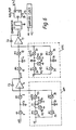
- Fig. 1 is a schematic block diagram representative of typical analog implementations according to the prior art.
- Fig. 2 is a schematic block diagram basically representative of switched capacitor implementations.
- Fig. 3 is a schematic diagram of an implementation of the DeLta-Sigma modulator according to the invention employing +V and -V reference voltages.
- Fig. 4 is a timing waveform presentation for the circuit of Fig. 3.
- Fig. 5 shows a portion of a circuit of Fig. 4 with circuitry adapated to the use of a single reference voltage +V.
- Fig. 6 iLLustrates the substitution of the single reference voltage circuitry of Fig. 5 into the device of Fig.3.
- At the outset, it should be pointed out that the term DeLta-Sigma modulator is sometimes called a Sigma-Delta modulator, the transposition of the sigma and delta terms being a matter of author's preference, the same device going under either name. Fig. 1 is prior art as aforementioned and substantially self-explanatory. In Fig. 1 herewith, the D/A converter would be a pulse shaper providing one of the two different pulses in accordance with whether the digital signal is high or low, mathematiclly +A or -A, the quantity A being related to the conversion between a number and a voltage. The basically Lowpass (integrating) device labeled H(s) determines the order of the DeLta-Sigma modulator. H(s) is typically a first order filter if H(s) is = 2 and second order s if

- It may be said that the modulator noise (inaccuracy of conversion of the input function to a digital signal) reduction achieved by the DeLta-Sigma modulator is the result of keeping track of all previous conversion errors and feeding this information (as an error related signal) back to correct the next conversion. In this process, a first order modulator attempts to zero the average error over a period of time, whereas a second order modulator not only keeps this average error at zero but also keeps the first derivative of the error signal at zero.
- In a first order system, only a DC input signal will be accurately represented digitally, However, in a second order system, the bandwidth of the signal which can be continuously represented digitally is increased.
- According to known filter theory, the integrating filter H(s) can be described for a first order DeLta-Sigma moduLator as:


- In Fig. 1 of that paper, the sampling pulse generator and pulse modulator together form an A/D + D/A operation. The pulse modulator outputs a pulse of known shape whose polarity is determined by the polarity of the analog signal at the input of the pulse modulator at the instant the sampling pulse is asserted.
- Higher order DeLta-Sigma modulators provide, potentially, better noise behavior but are notorious for being unstable and are consequently not recommended. The second order embodiment herein described is regarded as optimum.
- ALL switched capacitor implementations are generalized in Fig. 2 and can be, mathematically, reduced to the form shown below.
- H(z) is a discrete-time transfer function, of the form (for "second-order Delta-Sigma ModuLator"):

- The switched capacitor DeLta-Sigma modulator according to the invention is best explained in stages. The principle underlying the operation of any DeLta-Sigma modulator is to provide an anaLog-to-digitaL conversion wherein the digital word size is small but the sampling frequency is much higher than the highest signal (speech) frequency.
- First consider the sampling clock which operates the D type (edge-triggered) flip-flop, 20 in Fig. 3. This clock provides the time reference f and also two other clock waveforms, at the sampling frequency, but with duty cycle Less than 50 %. These are designated θ1 ("charge") and θ2 ("discharge"). Fig. 4 depicts these waveforms in a typical relationship.
- Consider next a section of Fig. 3 consisting of
switches sampling clock 303 controls theswitch 1 and 62 controls theswitch 3. When θ1 is Low,switch 1 is open (open circuit) and when θ1 is high,switch 1 is closed (short circuit). Similarly with θ2 andswitch 3. The non-overLapping nature of θ1 and θ2 ensures thatswitches 
switches 

- The dotted
enclosures 
- The noise performance and stability of the Delta-Sigma modulator is governed by the capacitor ratios

- The voltage V is termed the "reference voltag-e" and normally all voltages are evaluated as fractions thereof. V ist sometimes referred to as the "crash point" of the encoder and is the maximum amplitude of the input signal. An input amplitude of greater than V will cause overload.
- For a typical DeLta-Sigma modulator, the following capacitor ratios were found to be satisfactory.


- It will be noted that the configuration of Fig. 3 requires two reference voltages, +V and -V. If only one reference, for example +V is available, then the configuration consisting of +V, -V, switches 6, 7 and 9 and capacitor C2 (similarly with +V, -V, switches 13, 14, 16 and capacitor C5) can be replaced by the
circuit 501 shown in Fig. 5 and included in Fig. 6 asdotted block 601. - In that variation, and during each sampling interval, C8 charges to V during θ1 and during θ2 causing a change of - (

- During θ1, C7 charges to V volts with the polarity indicated shown on Figs. 5 and 6. If Qn were "high ", i.e., b(n) = +1, switches 23 and 22 would close during θ2 and, because of
the polarity reversal, cause a change of + (
- if


- If C7 = 2C8, then the overall operation of the circuit in Fig. 5 can be described as


- The samling rate must be much higher than the highest frequency component of the input signal u(t). The invention is particularly useful for digitally encoding telephone (speech) band signals for transmission through a discrete telephonic channel. Since such signals require only a few kHz of bandwidth, and accordingly the sampling rate of 1 MHz typical for the modulator of the invention fulfills the aforementioned requirement. A second order Delta-Sigma modulator can be considered to be constructed of a first orde-r DeLta-Sigma modulator embedded in a feedback Loop. Conversely, a first order DeLta-Sigma modulator can be considered to be a subset of a second order DeLta-Sigma modulator obtained by "stripping" the second order DeLta-Sigma moduLator down. The configuration shown in Figures 3 or 6 be stripped down to form a first order switched capacitor DeLta-Sigma modulator. If amplifier 4, capacitors C3, C1, C2 and their associated switches are removed, what remains is a first order DeLta-Sigma modulator which converts an analog signal at u into a digital signal b(n).
- It is possible to transmit the bit-stream {b(n)} as is and at the receiving end have a simple digital-to-analog converter which comprises of a pulse shaper which puts out distinct waveforms in a bit-inverval according as b(n) = "HIGH" or b(n) = "LOW" followed by a simple analog Lowpass filter to smooth the waveform. This, however, would entail the transmission of {b(n)} directly, which is about 1 megabit/s which is quite high. An alternative method, is to employ a sequence of digital Lowpass filters which do the "smooting" while retaining the digital nature of the signal. As a consequence, the number of bits per word increases, that is the granularity of levels, which can be represented, is made fine. In a Line circuit such as that of U.S. Patent No. 4,270,027 the Lowpass filters permit the resampling of the digital signal at 8 Kilowords per sec with a granularity corresponding to 13 bits per word in a uniform code. Each code word can be converted into an 8-bit code, if so desired, corresponding to either the A-law or µ-Law format. The 1-bit device, in this sense, does represent a Large range of sample values from u(nt). The 1-bit/word, 1 Mword/sec stream (i.e. a 1-Megabit/sec stream) is some- taimes referred to in the art as "PULSE-DENSITY MODULATED" version of the complex voice channel signal.
Claims (9)
Priority Applications (1)
| Application Number | Priority Date | Filing Date | Title |
|---|---|---|---|
| AT83100279T ATE37256T1 (en) | 1982-01-20 | 1983-01-14 | DELTA-SIGMA MODULATOR WITH SWITCHED CAPACITOR REALIZATION. |
Applications Claiming Priority (2)
| Application Number | Priority Date | Filing Date | Title |
|---|---|---|---|
| US06/340,931 US4439756A (en) | 1982-01-20 | 1982-01-20 | Delta-Sigma modulator with switch capacitor implementation |
| US340931 | 1989-04-20 |
Publications (3)
| Publication Number | Publication Date |
|---|---|
| EP0084353A2 true EP0084353A2 (en) | 1983-07-27 |
| EP0084353A3 EP0084353A3 (en) | 1985-08-14 |
| EP0084353B1 EP0084353B1 (en) | 1988-09-14 |
Family
ID=23335536
Family Applications (1)
| Application Number | Title | Priority Date | Filing Date |
|---|---|---|---|
| EP83100279A Expired EP0084353B1 (en) | 1982-01-20 | 1983-01-14 | Delta-sigma modulator with switched capacitor implementation |
Country Status (28)
| Country | Link |
|---|---|
| US (1) | US4439756A (en) |
| EP (1) | EP0084353B1 (en) |
| JP (1) | JPS58170115A (en) |
| KR (1) | KR900008049B1 (en) |
| AT (1) | ATE37256T1 (en) |
| AU (1) | AU557736B2 (en) |
| BE (1) | BE895656A (en) |
| BR (1) | BR8300195A (en) |
| CA (1) | CA1191958A (en) |
| DE (1) | DE3378008D1 (en) |
| EG (1) | EG15067A (en) |
| ES (1) | ES8500680A1 (en) |
| FI (1) | FI81223C (en) |
| GR (1) | GR78435B (en) |
| HU (1) | HU187522B (en) |
| IE (1) | IE55546B1 (en) |
| IN (1) | IN159353B (en) |
| IT (1) | IT1168702B (en) |
| MA (1) | MA19684A1 (en) |
| MX (1) | MX153054A (en) |
| NO (1) | NO158706C (en) |
| NZ (1) | NZ202845A (en) |
| PH (1) | PH19777A (en) |
| PT (1) | PT76126B (en) |
| RO (1) | RO84865B (en) |
| SU (1) | SU1336958A3 (en) |
| YU (1) | YU291882A (en) |
| ZA (1) | ZA829475B (en) |
Cited By (11)
| Publication number | Priority date | Publication date | Assignee | Title |
|---|---|---|---|---|
| EP0155061A2 (en) * | 1984-03-16 | 1985-09-18 | BELL TELEPHONE MANUFACTURING COMPANY Naamloze Vennootschap | Sigma-delta modulator |
| EP0208371A1 (en) * | 1985-07-02 | 1987-01-14 | Koninklijke Philips Electronics N.V. | Digital-to-analog converter |
| US4733219A (en) * | 1986-02-27 | 1988-03-22 | Alcatel N.V. | Converter circuit |
| FR2604839A1 (en) * | 1986-10-07 | 1988-04-08 | Crystal Semiconductor Corp | METHOD FOR REDUCING THE EFFECTS OF ELECTRICAL NOISE IN AN ANALOG TO DIGITAL CONVERTER |
| EP0328318A2 (en) * | 1988-02-10 | 1989-08-16 | Fujitsu Limited | Delta-sigma modulator |
| DE3908314A1 (en) * | 1988-03-15 | 1989-09-28 | Toshiba Kawasaki Kk | ANALOG-DIGITAL CONVERTER WITH DELTA SIGMA MODULATION |
| EP0396786A1 (en) * | 1989-05-08 | 1990-11-14 | Siemens Aktiengesellschaft | Integrable sigma-delta modulator of the switched-capacitor type |
| EP1735911A1 (en) * | 2004-03-31 | 2006-12-27 | Silicon Labs CP, Inc. | Gain control for delta sigma analog-to-digital converter |
| EP1777825A1 (en) * | 2005-10-21 | 2007-04-25 | Realtek Semiconductor Corp. | Low-pass filter based delta-sigma modulator |
| US7321325B2 (en) | 2005-07-07 | 2008-01-22 | Realtek Semiconductor Corp. | Background calibration of continuous-time delta-sigma modulator |
| US7446687B2 (en) | 2006-10-27 | 2008-11-04 | Realtek Semiconductor Corp. | Method and apparatus to reduce internal circuit errors in a multi-bit delta-sigma modulator |
Families Citing this family (36)
| Publication number | Priority date | Publication date | Assignee | Title |
|---|---|---|---|---|
| FR2533382B1 (en) * | 1982-09-21 | 1988-01-22 | Senn Patrice | DELTA-SIGMA, DOUBLE INTEGRATION ENCODER AND APPLICATIONS OF THIS ENCODER TO A MIC TYPE TRANSMISSION CHANNEL AND TO THE MEASUREMENT OF CONTINUOUS VOLTAGES |
| US4704600A (en) * | 1985-02-04 | 1987-11-03 | Nippon Telegraph And Telephone Corporation | Oversampling converter |
| US4654815A (en) * | 1985-02-07 | 1987-03-31 | Texas Instruments Incorporated | Analog signal conditioning and digitizing integrated circuit |
| US4675863A (en) | 1985-03-20 | 1987-06-23 | International Mobile Machines Corp. | Subscriber RF telephone system for providing multiple speech and/or data signals simultaneously over either a single or a plurality of RF channels |
| US4825448A (en) * | 1986-08-07 | 1989-04-25 | International Mobile Machines Corporation | Subscriber unit for wireless digital telephone system |
| US5010347A (en) * | 1987-09-25 | 1991-04-23 | Nec Corporation | Analog-to-digital converter having an excellent signal-to-noise ratio for small signals |
| US4851841A (en) * | 1987-10-02 | 1989-07-25 | Crystal Semiconductor Corporation | Gain scaling of oversampled analog-to-digital converters |
| US4876543A (en) * | 1988-05-31 | 1989-10-24 | Motorola, Inc. | Multi-rate cascaded noise shaping modulator |
| US5150324A (en) * | 1988-06-09 | 1992-09-22 | Asahi Kasei Microsystems Co. Ltd. | Analog arithmetic circuit that can perform multiplication division expansion and compression by using delta sigma modulator |
| US4924226A (en) * | 1988-07-29 | 1990-05-08 | Carillon Technology, Inc. | Signal error compensation |
| US4972436A (en) * | 1988-10-14 | 1990-11-20 | Hayes Microcomputer Products, Inc. | High performance sigma delta based analog modem front end |
| NL8901602A (en) * | 1989-06-23 | 1991-01-16 | Bronkhorst High Tech Bv | INTEGRATED SEMICONDUCTOR SWITCH FOR THERMAL MEASUREMENTS. |
| US5063521A (en) * | 1989-11-03 | 1991-11-05 | Motorola, Inc. | Neuram: neural network with ram |
| US5055843A (en) * | 1990-01-31 | 1991-10-08 | Analog Devices, Inc. | Sigma delta modulator with distributed prefiltering and feedback |
| US5159341A (en) * | 1991-03-12 | 1992-10-27 | Analog Devices, Inc. | Two phase sampling for a delta sigma modulator |
| US5287107A (en) * | 1992-06-05 | 1994-02-15 | Hewlett-Packard Company | Optical isolation amplifier with sigma-delta modulation |
| US5719572A (en) * | 1994-07-08 | 1998-02-17 | Cirrus Logic, Inc. | Digital signal processor with reduced pattern dependent noise |
| US5801652A (en) * | 1994-07-08 | 1998-09-01 | Cirrus Logic, Inc. | Pattern dependent noise reduction in a digital processing circuit utilizing image circuitry |
| KR0155622B1 (en) * | 1995-05-02 | 1998-12-15 | 문정환 | Delta-sigma a/d converter |
| US5771281A (en) * | 1995-05-02 | 1998-06-23 | Batten, Jr.; George Washington | Serial-port powered caller identification computer interface |
| US5760723A (en) * | 1996-06-10 | 1998-06-02 | General Electric Company | Delta-sigma analog-to-digital converter including charge coupled devices |
| US6035005A (en) * | 1997-02-10 | 2000-03-07 | Motorola, Inc. | Receiver with baseband I and Q demodulator |
| CA2213156A1 (en) * | 1997-08-15 | 1999-02-15 | Philsar Electronics Inc. | One bit digital quadrature vector modulator |
| US6275259B1 (en) * | 1998-02-02 | 2001-08-14 | International Business Machines Corporation | Digital automatic gain control circuit for image system |
| US6160505A (en) * | 1998-02-24 | 2000-12-12 | At&T Corp | Method and apparatus for converting an analog signal to a digital signal |
| GB2335322B (en) * | 1998-03-13 | 2002-04-24 | Ericsson Telefon Ab L M | Phase detector |
| US6087969A (en) * | 1998-04-27 | 2000-07-11 | Motorola, Inc. | Sigma-delta modulator and method for digitizing a signal |
| US6816100B1 (en) | 1999-03-12 | 2004-11-09 | The Regents Of The University Of California | Analog-to-digital converters with common-mode rejection dynamic element matching, including as used in delta-sigma modulators |
| JP3407871B2 (en) * | 1999-09-17 | 2003-05-19 | 日本電気株式会社 | Analog / digital mixed ΔΣ modulator |
| CA2292463C (en) * | 1999-12-17 | 2005-04-12 | Vtech Communications, Ltd. | Digitally-implemented demodulator |
| KR20010096789A (en) * | 2000-04-14 | 2001-11-08 | 조양호 | Sigma-delta modulator with efficient clock speeds |
| KR20020035586A (en) * | 2000-07-07 | 2002-05-11 | 롤페스 요하네스 게라투스 알베르투스 | Sigma-delta modulator with an adjustable feedback factor |
| JP4845038B2 (en) * | 2007-03-01 | 2011-12-28 | 敏雄 鈴木 | Steel coil fall prevention tool and fall prevention method |
| US7915838B2 (en) * | 2007-06-29 | 2011-03-29 | Cypress Semiconductor Corporation | Delta-sigma signal density modulation for optical transducer control |
| US7646325B2 (en) * | 2007-09-27 | 2010-01-12 | Nanoamp Mobile, Inc. | Analog to digital converter |
| US7916054B2 (en) * | 2008-11-07 | 2011-03-29 | Baker R Jacob | K-delta-1-sigma modulator |
Citations (4)
| Publication number | Priority date | Publication date | Assignee | Title |
|---|---|---|---|---|
| EP0023182A1 (en) * | 1979-07-20 | 1981-01-28 | Jean-Pierre Petit | Digital transmission system with delta-sigma coder with double analogue integration and delta-sigma decoder with double digital integration |
| JPS5625827A (en) * | 1979-08-10 | 1981-03-12 | Nec Corp | Coding unit |
| WO1982004508A1 (en) * | 1981-06-12 | 1982-12-23 | Inc Gould | Enhanced delta modulation encoder |
| EP0104988A1 (en) * | 1982-09-21 | 1984-04-04 | Patrice Senn | Double integration delta-sigma encoder and use of this encoder in a PCM transmission path and in the measuring of DC voltages |
Family Cites Families (2)
| Publication number | Priority date | Publication date | Assignee | Title |
|---|---|---|---|---|
| US4009475A (en) * | 1974-12-05 | 1977-02-22 | Hybrid Systems Corporation | Delta-sigma converter and decoder |
| US4270027A (en) * | 1979-11-28 | 1981-05-26 | International Telephone And Telegraph Corporation | Telephone subscriber line unit with sigma-delta digital to analog converter |
-
1982
- 1982-01-20 US US06/340,931 patent/US4439756A/en not_active Expired - Lifetime
- 1982-12-10 PH PH28258A patent/PH19777A/en unknown
- 1982-12-15 AU AU91545/82A patent/AU557736B2/en not_active Expired
- 1982-12-17 NZ NZ202845A patent/NZ202845A/en unknown
- 1982-12-22 SU SU823526948A patent/SU1336958A3/en active
- 1982-12-23 ZA ZA829475A patent/ZA829475B/en unknown
- 1982-12-30 YU YU02918/82A patent/YU291882A/en unknown
-
1983
- 1983-01-10 KR KR1019830000066A patent/KR900008049B1/en active IP Right Grant
- 1983-01-11 GR GR70236A patent/GR78435B/el unknown
- 1983-01-14 EP EP83100279A patent/EP0084353B1/en not_active Expired
- 1983-01-14 DE DE8383100279T patent/DE3378008D1/en not_active Expired
- 1983-01-14 AT AT83100279T patent/ATE37256T1/en not_active IP Right Cessation
- 1983-01-17 BR BR8300195A patent/BR8300195A/en not_active IP Right Cessation
- 1983-01-17 HU HU83138A patent/HU187522B/en not_active IP Right Cessation
- 1983-01-17 RO RO109753A patent/RO84865B/en unknown
- 1983-01-17 MA MA19901A patent/MA19684A1/en unknown
- 1983-01-18 EG EG34/83A patent/EG15067A/en active
- 1983-01-18 NO NO830149A patent/NO158706C/en unknown
- 1983-01-19 IE IE104/83A patent/IE55546B1/en not_active IP Right Cessation
- 1983-01-19 MX MX195962A patent/MX153054A/en unknown
- 1983-01-19 CA CA000419747A patent/CA1191958A/en not_active Expired
- 1983-01-20 ES ES519149A patent/ES8500680A1/en not_active Expired
- 1983-01-20 FI FI830182A patent/FI81223C/en not_active IP Right Cessation
- 1983-01-20 JP JP58007998A patent/JPS58170115A/en active Granted
- 1983-01-20 PT PT76126A patent/PT76126B/en not_active IP Right Cessation
- 1983-01-20 IT IT19189/83A patent/IT1168702B/en active
- 1983-01-20 BE BE2/60001A patent/BE895656A/en not_active IP Right Cessation
- 1983-08-10 IN IN993/CAL/83A patent/IN159353B/en unknown
Patent Citations (4)
| Publication number | Priority date | Publication date | Assignee | Title |
|---|---|---|---|---|
| EP0023182A1 (en) * | 1979-07-20 | 1981-01-28 | Jean-Pierre Petit | Digital transmission system with delta-sigma coder with double analogue integration and delta-sigma decoder with double digital integration |
| JPS5625827A (en) * | 1979-08-10 | 1981-03-12 | Nec Corp | Coding unit |
| WO1982004508A1 (en) * | 1981-06-12 | 1982-12-23 | Inc Gould | Enhanced delta modulation encoder |
| EP0104988A1 (en) * | 1982-09-21 | 1984-04-04 | Patrice Senn | Double integration delta-sigma encoder and use of this encoder in a PCM transmission path and in the measuring of DC voltages |
Non-Patent Citations (4)
| Title |
|---|
| ELECRONIC ENGINEERING, vol. 50, no. 602, February 1978, pages 17-19, London, GB; "A.E. WHITTAKER: "Chopped complementary deltaverter" * |
| IEEE INTERNATIONAL CONFERENCE ON ACOUSTICS, SPEECH AND SIGNAL PROCESSING, ICASSP 82, 3rd-5th May 1982, Paris, France, vol. 3, pages 1980-1983, IEEE, New York, US; B.P. AGRAWAL et al.: "Specification-based design of epsilon-delta-mu for A/D and D/A conversion" * |
| IEEE JOURNAL OF SOLID-STATE CIRCUITS, vol. SC-12, no. 6, December 1977, pages 600-608, New York, US; B.J. HOSTICKA et al.: "MOS sampled data recursive filters using switched capacitor integrators" * |
| PATENTS ABSTRACTS OF JAPAN; Vol. 5, no. 78 (E58)[750], 22nd May 1981; & JP-A-56 025 827 (NIPPON DENKI K.K.) 12-03-1981 * |
Cited By (17)
| Publication number | Priority date | Publication date | Assignee | Title |
|---|---|---|---|---|
| EP0155061A2 (en) * | 1984-03-16 | 1985-09-18 | BELL TELEPHONE MANUFACTURING COMPANY Naamloze Vennootschap | Sigma-delta modulator |
| EP0155061A3 (en) * | 1984-03-16 | 1987-05-13 | Bell Telephone Manufacturing Company Naamloze Vennootschap | Switched capacitance feedback control circuit and sigma-delta modulator using same |
| EP0208371A1 (en) * | 1985-07-02 | 1987-01-14 | Koninklijke Philips Electronics N.V. | Digital-to-analog converter |
| US4733219A (en) * | 1986-02-27 | 1988-03-22 | Alcatel N.V. | Converter circuit |
| FR2604839A1 (en) * | 1986-10-07 | 1988-04-08 | Crystal Semiconductor Corp | METHOD FOR REDUCING THE EFFECTS OF ELECTRICAL NOISE IN AN ANALOG TO DIGITAL CONVERTER |
| EP0328318A2 (en) * | 1988-02-10 | 1989-08-16 | Fujitsu Limited | Delta-sigma modulator |
| EP0328318A3 (en) * | 1988-02-10 | 1990-11-14 | Fujitsu Limited | Delta-sigma modulator |
| DE3908314A1 (en) * | 1988-03-15 | 1989-09-28 | Toshiba Kawasaki Kk | ANALOG-DIGITAL CONVERTER WITH DELTA SIGMA MODULATION |
| EP0396786A1 (en) * | 1989-05-08 | 1990-11-14 | Siemens Aktiengesellschaft | Integrable sigma-delta modulator of the switched-capacitor type |
| EP1735911A1 (en) * | 2004-03-31 | 2006-12-27 | Silicon Labs CP, Inc. | Gain control for delta sigma analog-to-digital converter |
| EP1735911A4 (en) * | 2004-03-31 | 2007-08-08 | Silicon Labs Cp Inc | Gain control for delta sigma analog-to-digital converter |
| US7315200B2 (en) | 2004-03-31 | 2008-01-01 | Silicon Labs Cp, Inc. | Gain control for delta sigma analog-to-digital converter |
| US7321325B2 (en) | 2005-07-07 | 2008-01-22 | Realtek Semiconductor Corp. | Background calibration of continuous-time delta-sigma modulator |
| EP1777825A1 (en) * | 2005-10-21 | 2007-04-25 | Realtek Semiconductor Corp. | Low-pass filter based delta-sigma modulator |
| US7277032B2 (en) | 2005-10-21 | 2007-10-02 | Realtek Semiconductor Corp. | Low-pass filter based delta-sigma modulator |
| US7301489B2 (en) | 2005-10-21 | 2007-11-27 | Realtek Semiconductor Corp. | Dithering noise cancellation for a delta-sigma modulator |
| US7446687B2 (en) | 2006-10-27 | 2008-11-04 | Realtek Semiconductor Corp. | Method and apparatus to reduce internal circuit errors in a multi-bit delta-sigma modulator |
Also Published As
Similar Documents
| Publication | Publication Date | Title |
|---|---|---|
| EP0084353B1 (en) | Delta-sigma modulator with switched capacitor implementation | |
| KR910009070B1 (en) | Delta to sigma converter | |
| EP2026468B1 (en) | High precision analog to digital converter | |
| US5563597A (en) | Switched-capacitor one-bit digital-to-analog converter with low sensitivity to op-amp offset voltage | |
| EP0199745B1 (en) | Analog-to-digital converter | |
| US5896101A (en) | Wide dynamic range delta sigma A/D converter | |
| KR100928406B1 (en) | Incremental-Delta Analog-to-Digital Conversion | |
| US6369730B1 (en) | Sigma-delta analog-to-digital converter | |
| EP0241077A1 (en) | Encoding device | |
| JPH09510056A (en) | Sigma-delta converter with digital logic gate core | |
| EP0642221A1 (en) | Output filter for over-sampling digital-to-analog converter | |
| Paulos et al. | Improved signal-to-noise ratio using tri-level delta-sigma modulation | |
| EP0208371A1 (en) | Digital-to-analog converter | |
| JP3009597B2 (en) | Multi-bit ΔΣ digital / analog converter | |
| EP0367522A2 (en) | Closed loop pulse width analog-to-digital converter | |
| EP0190694A2 (en) | Oversampling converter | |
| US3959745A (en) | Pulse amplitude modulator | |
| TWI831150B (en) | Sigma delta modulator | |
| CS276581B6 (en) | Delta-sigma modulator | |
| JPH06318872A (en) | Deltasigma modulator | |
| TW202339442A (en) | Sigma delta modulator | |
| CN116846400A (en) | Delta-sigma modulator | |
| JPH02170723A (en) | A/d converting circuit | |
| Baccigalupi et al. | A variable sampling rate third order MASH/spl Sigma//spl Delta/modulator for measurement applications |
Legal Events
| Date | Code | Title | Description |
|---|---|---|---|
| PUAI | Public reference made under article 153(3) epc to a published international application that has entered the european phase |
Free format text: ORIGINAL CODE: 0009012 |
|
| AK | Designated contracting states |
Designated state(s): AT CH DE FR GB LI NL SE |
|
| PUAL | Search report despatched |
Free format text: ORIGINAL CODE: 0009013 |
|
| AK | Designated contracting states |
Designated state(s): AT CH DE FR GB LI NL SE |
|
| 17P | Request for examination filed |
Effective date: 19851114 |
|
| 17Q | First examination report despatched |
Effective date: 19861219 |
|
| RAP1 | Party data changed (applicant data changed or rights of an application transferred) |
Owner name: ALCATEL N.V. |
|
| RAP3 | Party data changed (applicant data changed or rights of an application transferred) |
Owner name: ALCATEL N.V. |
|
| GRAA | (expected) grant |
Free format text: ORIGINAL CODE: 0009210 |
|
| AK | Designated contracting states |
Kind code of ref document: B1 Designated state(s): AT CH DE FR GB LI NL SE |
|
| REF | Corresponds to: |
Ref document number: 37256 Country of ref document: AT Date of ref document: 19880915 Kind code of ref document: T |
|
| REF | Corresponds to: |
Ref document number: 3378008 Country of ref document: DE Date of ref document: 19881020 |
|
| ET | Fr: translation filed | ||
| PLBE | No opposition filed within time limit |
Free format text: ORIGINAL CODE: 0009261 |
|
| STAA | Information on the status of an ep patent application or granted ep patent |
Free format text: STATUS: NO OPPOSITION FILED WITHIN TIME LIMIT |
|
| 26N | No opposition filed | ||
| PGFP | Annual fee paid to national office [announced via postgrant information from national office to epo] |
Ref country code: DE Payment date: 19930227 Year of fee payment: 11 |
|
| PGFP | Annual fee paid to national office [announced via postgrant information from national office to epo] |
Ref country code: CH Payment date: 19930415 Year of fee payment: 11 |
|
| PGFP | Annual fee paid to national office [announced via postgrant information from national office to epo] |
Ref country code: FR Payment date: 19931230 Year of fee payment: 12 |
|
| PGFP | Annual fee paid to national office [announced via postgrant information from national office to epo] |
Ref country code: GB Payment date: 19940105 Year of fee payment: 12 |
|
| PGFP | Annual fee paid to national office [announced via postgrant information from national office to epo] |
Ref country code: SE Payment date: 19940127 Year of fee payment: 12 |
|
| PG25 | Lapsed in a contracting state [announced via postgrant information from national office to epo] |
Ref country code: LI Effective date: 19940131 Ref country code: CH Effective date: 19940131 |
|
| PGFP | Annual fee paid to national office [announced via postgrant information from national office to epo] |
Ref country code: NL Payment date: 19940131 Year of fee payment: 12 |
|
| REG | Reference to a national code |
Ref country code: CH Ref legal event code: PL |
|
| PG25 | Lapsed in a contracting state [announced via postgrant information from national office to epo] |
Ref country code: DE Effective date: 19941001 |
|
| PGFP | Annual fee paid to national office [announced via postgrant information from national office to epo] |
Ref country code: AT Payment date: 19950105 Year of fee payment: 13 |
|
| PG25 | Lapsed in a contracting state [announced via postgrant information from national office to epo] |
Ref country code: GB Effective date: 19950114 |
|
| PG25 | Lapsed in a contracting state [announced via postgrant information from national office to epo] |
Ref country code: SE Effective date: 19950115 |
|
| EAL | Se: european patent in force in sweden |
Ref document number: 83100279.5 |
|
| PG25 | Lapsed in a contracting state [announced via postgrant information from national office to epo] |
Ref country code: NL Effective date: 19950801 |
|
| GBPC | Gb: european patent ceased through non-payment of renewal fee |
Effective date: 19950114 |
|
| PG25 | Lapsed in a contracting state [announced via postgrant information from national office to epo] |
Ref country code: FR Effective date: 19950929 |
|
| NLV4 | Nl: lapsed or anulled due to non-payment of the annual fee |
Effective date: 19950801 |
|
| EUG | Se: european patent has lapsed |
Ref document number: 83100279.5 |
|
| REG | Reference to a national code |
Ref country code: FR Ref legal event code: ST |
|
| PG25 | Lapsed in a contracting state [announced via postgrant information from national office to epo] |
Ref country code: AT Effective date: 19960114 |