EP0084231A1 - Vortex shedding flowmeter circuit arrangements - Google Patents
Vortex shedding flowmeter circuit arrangements Download PDFInfo
- Publication number
- EP0084231A1 EP0084231A1 EP82306579A EP82306579A EP0084231A1 EP 0084231 A1 EP0084231 A1 EP 0084231A1 EP 82306579 A EP82306579 A EP 82306579A EP 82306579 A EP82306579 A EP 82306579A EP 0084231 A1 EP0084231 A1 EP 0084231A1
- Authority
- EP
- European Patent Office
- Prior art keywords
- pulse
- signal
- fixed width
- vortex shedding
- circuit arrangement
- Prior art date
- Legal status (The legal status is an assumption and is not a legal conclusion. Google has not performed a legal analysis and makes no representation as to the accuracy of the status listed.)
- Granted
Links
Images

Classifications
-
- G—PHYSICS
- G01—MEASURING; TESTING
- G01F—MEASURING VOLUME, VOLUME FLOW, MASS FLOW OR LIQUID LEVEL; METERING BY VOLUME
- G01F1/00—Measuring the volume flow or mass flow of fluid or fluent solid material wherein the fluid passes through a meter in a continuous flow
- G01F1/05—Measuring the volume flow or mass flow of fluid or fluent solid material wherein the fluid passes through a meter in a continuous flow by using mechanical effects
- G01F1/20—Measuring the volume flow or mass flow of fluid or fluent solid material wherein the fluid passes through a meter in a continuous flow by using mechanical effects by detection of dynamic effects of the flow
- G01F1/32—Measuring the volume flow or mass flow of fluid or fluent solid material wherein the fluid passes through a meter in a continuous flow by using mechanical effects by detection of dynamic effects of the flow using swirl flowmeters
- G01F1/325—Means for detecting quantities used as proxy variables for swirl
- G01F1/3287—Means for detecting quantities used as proxy variables for swirl circuits therefor
Definitions
- This invention relates to vortex shedding flowmeter circuit arrangements.
- Vortex shedding flowmeters are known.
- an obstruction or bluff body is positioned in a fluid flow.
- Vortices are generated at alternate sides of the obstruction with a frequency which is proportional to the volumetric flow rate.
- the passage of the vortices is counted to provide a signal which indicates the flow rate.
- Such a flowmeter is disclosed for example in US Patents No 4 094 194 (Herzl).
- a vortex shedding flowmeter circuit arrangement including a vortex sensor for generating a vortex shedding frequency signal, the arrangement being characterised by pulse means connected to the vortex sensor for generating a fixed width pulse with a frequency equal to the vortex shedding frequency signal, and a low pass filter connected to the pulse means for receiving the fixed width pulse and operative to generate an analog signal which is proportional in level to the vortex shedding frequency signal.
- a preferred embodiment of the present invention described hereinbelow provides a circuit arrangement for processing a vortex shedding flowmeter signal which produces output signals that are directly compatible with digital control systems.
- the preferred circuit arrangement in fact generates both an analog and a pulse signal, both of which are proportional to the vortex shedding frequency signal.
- the vortex shedding frequency signal is preamplified and supplied to a one-shot for producing pulses, which pulses are processed through a low pass filter to produce the analog signal which is proportional to the vortex shedding frequency.
- the pulse signal is tapped directly from the one-shot to produce a pulse frequency signal having a frequency proportional to the vortex shedding frequency.
- Both the analog and pulse signals typically have a 4 to 20 mA output, which is compatible with known two wire transmission systems for vortex shedding flowmeters.
- the preferred circuit arrangement includes a range selection circuit for receiving the pulse signal to scale or change the range of measurement of the vortex shedding flowmeter.
- the preferred circuit arrangement is simple in design and economical to manufacture.
- FIG. 1 of the drawings shows a vortex shedding flowmeter circuit arrangement having a vortex sensor 10 which generates an output in the form of a vortex shedding frequency signal that has a frequency corresponding to the vortex shedding frequency of a vortex shedding flowmeter.
- the output of the vortex sensor 10 is supplied over a preamplifier 12 to a threshold detector 14.
- An output of the threshold detector 14 is supplied to a one-shot (monostable multivibrator) 16 which generates a fixed width pulse for each cycle of the vortex frequency.
- An output of the one-shot 16 is supplied to a low pass filter 20 for generating an analog signal at a terminal 18, and to a pulse signal network 22 which generates a pulse signal at a terminal 24.
- the low pass filter 20 converts the fixed width pulse coming from the one-shot 16 into an analog level corresponding to the rate of pulses. This thus corresponds to the vortex shedding frequency.
- Figure 2 shows an output stage which can be connected to the pulse signal terminal 24 and the analog signal terminal 18.
- the analog and pulse signals can be selected by a switch SA to apply either one or both of the signals to a non-inverting (positive) input of an operational amplifier OA 1 .
- the output stage of Figure 2 controls the current in two lines attached to terminals T 1 and T 2 . These lines contain a power supply designated 26 and current sensor means (not shown) at an opposite end of transmission lines connected to the terminals T 1 and T 2 .
- a transistor Q 1 and resistors R 32 R 4 are connected as shown between the terminals T 1 and T 2 .
- the resistor R 4 senses the current flowing between the terminals T 1 and T 2 and develops a voltage proportional to that current.
- Resistors R 1 and R 2 feed back a fraction of this voltage to the non-inverting (negative) input of the amplifier OA 1 .
- the amplifier OA 1 compares the input signal and the feedback signal and adjusts the loop including its own gain and the transistor Q 1 so that the two voltages are made equal. This action renders the output current proportional to the input signal of this circuit stage.
- the input signal is either an analog level, yielding a 4 to 20 mA output signal, or a pulse signal, yielding a pulsed output traversing the range of 4 to 20 mA, equalling approximately 4 mA with the pulse off and approximately 20 mA with the pulse on.
- These two inputs, analog or pulse are selected typically by the switch S A or by the movement of a plug cable jumper.
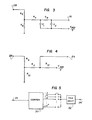
- FIG 3 shows an embodiment of the low pass filter 20 of Figure 1.
- the low pass filter 20 is used to smooth or average the fixed width pulses from the one-shot 16.
- a filtering action is effected by resistance and capacitor combinations R 7 , C 1 and R 8 , C2.
- the voltage at the non-inverting input of the amplifier OA 1 may not be a circuit common.
- the voltage V 1 across the resistor R 2 in Figure 2 will appear across the capacitors C 1 and C 2 in the low pass filter 20. Since these units typically have large values of capacitance and have leakage associated with them, they should have no dc voltage across them to encourage leakage. This leakage has severe effects on the accuracy of the signal for the 4 to 20 mA arrangement.
- V 1 is equal to one half of a reference voltage V REF ( Figure 2).
- V REF reference voltage
- the capacitors C l and C 2 are returned to a value of VREF/2 ( Figure 3).
- Resistors R 5 and R6 are selected so that the voltage at their junction equals one half the reference voltage when the one-shot 16 is off. A minimum of voltage is thus provided at the capacitors C l and C 2 to minimise leakage problems.
- Figure 4 is a schematic representation of an embodiment of pulse signal network 22 of Figure 1.
- the network 22 generates a pulsed frequency signal base level and amplitude.
- Resistors R 9 and R 10 form a voltage V REF /2 at their junction in a similar manner to the resistors R 5 and R 6 in Figure 3.
- the circuit of Figure 4 can actually be incorporated into the circuit of Figure 3, utilising the resistors R 5 and R 6 .
- Resistors R 11 and R12 select a fraction of the excursion of the pulse voltage at the junction between the resistors R 9 and R 10 and presented to the output stage at levels (pulse off and pulse on) to yield pulses between 4 mA (off) and 20 mA (on) in the output circuit.
- Scaling or range selection can be achieved using a circuit shown in Figure 5.
- This circuit contains a counter 30 which divides the vortex shedding frequency by a factor of 2 n , where n equals 1 to a maximum desired in the circuit. More specifically, as shown, the counter 30 may be arranged to divide the vortex shedding frequency by any one of a variety of factors 2 n , each having a different value of n.
- a following one-shot 32 generates a narrow pulse for the output, although it would instead be possible to transmit a 50% duty cycle waveform.
- the circuit of Figure 5 is typically used between those of Figures 2 and 4.
- the circuit of Figure 5 is shown connected between a terminal 24 of Figure 4 (Figure 1) and another terminal 24' which can be connected to the terminal 24 of Figure 2.
- CMOS integrated circuits are used.
- the one-shots are typically MC14538 units and the counter is typically a CD4024B.
- the amplifiers are typically OP20 units or LM108/308 units.
Landscapes
- Physics & Mathematics (AREA)
- Fluid Mechanics (AREA)
- General Physics & Mathematics (AREA)
- Measuring Volume Flow (AREA)
- Arrangements For Transmission Of Measured Signals (AREA)
Abstract
Description
- This invention relates to vortex shedding flowmeter circuit arrangements.
- Vortex shedding flowmeters are known. In such flowmeters, an obstruction or bluff body is positioned in a fluid flow. Vortices are generated at alternate sides of the obstruction with a frequency which is proportional to the volumetric flow rate. The passage of the vortices is counted to provide a signal which indicates the flow rate. Such a flowmeter is disclosed for example in US Patents No 4 094 194 (Herzl).
- It is also known to use a two wire transmission line for supplying power to and receiving a signal from a vortex shedding flowmeter. Such a transmission line arrangement is disclosed for example in US Patent Nos 4 123 940 (Herzl et al) and 4 134 297 (Herzl).
- In prior art circuitry for processing a signal from a vortex shedding flowmeter, it has been necessary to provide an interface between vortex sensing equipment providing the signal and digital control systems for processing the signal.
- According to the present invention there is provided a vortex shedding flowmeter circuit arrangement including a vortex sensor for generating a vortex shedding frequency signal, the arrangement being characterised by pulse means connected to the vortex sensor for generating a fixed width pulse with a frequency equal to the vortex shedding frequency signal, and a low pass filter connected to the pulse means for receiving the fixed width pulse and operative to generate an analog signal which is proportional in level to the vortex shedding frequency signal.
- A preferred embodiment of the present invention described hereinbelow provides a circuit arrangement for processing a vortex shedding flowmeter signal which produces output signals that are directly compatible with digital control systems. The preferred circuit arrangement in fact generates both an analog and a pulse signal, both of which are proportional to the vortex shedding frequency signal. The vortex shedding frequency signal is preamplified and supplied to a one-shot for producing pulses, which pulses are processed through a low pass filter to produce the analog signal which is proportional to the vortex shedding frequency. The pulse signal is tapped directly from the one-shot to produce a pulse frequency signal having a frequency proportional to the vortex shedding frequency. Both the analog and pulse signals typically have a 4 to 20 mA output, which is compatible with known two wire transmission systems for vortex shedding flowmeters. The preferred circuit arrangement includes a range selection circuit for receiving the pulse signal to scale or change the range of measurement of the vortex shedding flowmeter. The preferred circuit arrangement is simple in design and economical to manufacture.
- The invention will now be further described, by way of illustrative and non-limiting example, with reference to the accompanying drawings, in which:
- Figure 1 is a block diagram of an analog and pulse vortex shedding flowmeter circuit arrangement embodying the invention;
- Figure 2 is a schematic representation of an output stage for receiving an analog and a pulse signal from the circuit arrangement of Figure 1;
- Figure 3 is a schematic representation of a low pass filter that can be used in the circuit arrangement of Figure 1;
- Figure 4 is a schematic representation of a pulse signal network that can be used in the circuit arrangement of Figure 1; and
- Figure 5 is a block diagram of a pulse frequency range selection circuit which can be connected between the pulse signal network of Figure 4 and the output stage of Figure 2.
- Figure 1 of the drawings shows a vortex shedding flowmeter circuit arrangement having a
vortex sensor 10 which generates an output in the form of a vortex shedding frequency signal that has a frequency corresponding to the vortex shedding frequency of a vortex shedding flowmeter. The output of thevortex sensor 10 is supplied over apreamplifier 12 to athreshold detector 14. An output of thethreshold detector 14 is supplied to a one-shot (monostable multivibrator) 16 which generates a fixed width pulse for each cycle of the vortex frequency. An output of the one-shot 16 is supplied to alow pass filter 20 for generating an analog signal at aterminal 18, and to apulse signal network 22 which generates a pulse signal at aterminal 24. - The
low pass filter 20 converts the fixed width pulse coming from the one-shot 16 into an analog level corresponding to the rate of pulses. This thus corresponds to the vortex shedding frequency. - Figure 2 shows an output stage which can be connected to the
pulse signal terminal 24 and theanalog signal terminal 18. The analog and pulse signals can be selected by a switch SA to apply either one or both of the signals to a non-inverting (positive) input of an operational amplifier OA1. - The output stage of Figure 2 controls the current in two lines attached to terminals T1 and T2. These lines contain a power supply designated 26 and current sensor means (not shown) at an opposite end of transmission lines connected to the terminals T1 and T2.
- A transistor Q1 and resistors R32 R4 are connected as shown between the terminals T1 and T2. The resistor R4 senses the current flowing between the terminals T1 and T2 and develops a voltage proportional to that current. Resistors R1 and R2 feed back a fraction of this voltage to the non-inverting (negative) input of the amplifier OA1. The amplifier OA1 compares the input signal and the feedback signal and adjusts the loop including its own gain and the transistor Q1 so that the two voltages are made equal. This action renders the output current proportional to the input signal of this circuit stage. The input signal is either an analog level, yielding a 4 to 20 mA output signal, or a pulse signal, yielding a pulsed output traversing the range of 4 to 20 mA, equalling approximately 4 mA with the pulse off and approximately 20 mA with the pulse on. These two inputs, analog or pulse, are selected typically by the switch SA or by the movement of a plug cable jumper.
- Figure 3 shows an embodiment of the
low pass filter 20 of Figure 1. Thelow pass filter 20 is used to smooth or average the fixed width pulses from the one-shot 16. A filtering action is effected by resistance and capacitor combinations R7, C1 and R8, C2. In the output stage of Figure 2, the voltage at the non-inverting input of the amplifier OA1 may not be a circuit common. In this instance, the voltage V1 across the resistor R2 in Figure 2 will appear across the capacitors C1 and C2 in thelow pass filter 20. Since these units typically have large values of capacitance and have leakage associated with them, they should have no dc voltage across them to encourage leakage. This leakage has severe effects on the accuracy of the signal for the 4 to 20 mA arrangement. For optiumum sensitivity, V1 is equal to one half of a reference voltage V REF (Figure 2). Thus, the capacitors Cl and C2 are returned to a value of VREF/2 (Figure 3). Resistors R5 and R6 are selected so that the voltage at their junction equals one half the reference voltage when the one-shot 16 is off. A minimum of voltage is thus provided at the capacitors Cl and C2 to minimise leakage problems. - Figure 4 is a schematic representation of an embodiment of
pulse signal network 22 of Figure 1. Thenetwork 22 generates a pulsed frequency signal base level and amplitude. Resistors R9 and R10 form a voltage VREF/2 at their junction in a similar manner to the resistors R5 and R6 in Figure 3. The circuit of Figure 4 can actually be incorporated into the circuit of Figure 3, utilising the resistors R5 and R6. - Resistors R11 and R12 select a fraction of the excursion of the pulse voltage at the junction between the resistors R9 and R10 and presented to the output stage at levels (pulse off and pulse on) to yield pulses between 4 mA (off) and 20 mA (on) in the output circuit.
- Scaling or range selection can be achieved using a circuit shown in Figure 5. This circuit contains a
counter 30 which divides the vortex shedding frequency by a factor of 2n, where n equals 1 to a maximum desired in the circuit. More specifically, as shown, thecounter 30 may be arranged to divide the vortex shedding frequency by any one of a variety offactors 2n, each having a different value of n. A following one-shot 32 generates a narrow pulse for the output, although it would instead be possible to transmit a 50% duty cycle waveform. The circuit of Figure 5 is typically used between those of Figures 2 and 4. - In Figures 3 and 4, the
output 28 of the one-shot 16 from Figure 1 is shown connected to the input of each respective circuit. - The circuit of Figure 5 is shown connected between a
terminal 24 of Figure 4 (Figure 1) and another terminal 24' which can be connected to theterminal 24 of Figure 2. - Wherever possible to keep power consumption low, since only the 4 mA of the 4 to 20 mA is available to operate a circuit, CMOS integrated circuits are used.
- The one-shots are typically MC14538 units and the counter is typically a CD4024B. The amplifiers are typically OP20 units or LM108/308 units.
- Elements such as the vortex sensor, preamplifier and threshold detector of Figure 1 are known in the art as off-the-shelf items.
Claims (6)
Applications Claiming Priority (2)
| Application Number | Priority Date | Filing Date | Title |
|---|---|---|---|
| US06/329,531 US4429582A (en) | 1981-12-10 | 1981-12-10 | Vortex shedding flowmeter circuit with analog and pulse output signal |
| US329531 | 1989-03-28 |
Publications (2)
| Publication Number | Publication Date |
|---|---|
| EP0084231A1 true EP0084231A1 (en) | 1983-07-27 |
| EP0084231B1 EP0084231B1 (en) | 1986-08-27 |
Family
ID=23285843
Family Applications (1)
| Application Number | Title | Priority Date | Filing Date |
|---|---|---|---|
| EP82306579A Expired EP0084231B1 (en) | 1981-12-10 | 1982-12-09 | Vortex shedding flowmeter circuit arrangements |
Country Status (5)
| Country | Link |
|---|---|
| US (1) | US4429582A (en) |
| EP (1) | EP0084231B1 (en) |
| JP (2) | JPS58154619A (en) |
| CA (1) | CA1187312A (en) |
| DE (1) | DE3272944D1 (en) |
Cited By (1)
| Publication number | Priority date | Publication date | Assignee | Title |
|---|---|---|---|---|
| GB2177204A (en) * | 1985-06-26 | 1987-01-14 | British Gas Corp | Measurement of fluid flows |
Citations (4)
| Publication number | Priority date | Publication date | Assignee | Title |
|---|---|---|---|---|
| DE2632553A1 (en) * | 1976-07-20 | 1978-01-26 | Nord Micro Elektronik Feinmech | DEVICE FOR MEASURING THE VELOCITY OF FLOW BY USING SOUND |
| US4134297A (en) * | 1977-02-14 | 1979-01-16 | Fischer & Porter Company | Two-wire transmission system for vortex-type flowmeters |
| GB2008752A (en) * | 1977-11-14 | 1979-06-06 | Yokogawa Electric Works Ltd | Vortex flow meter |
| GB1566790A (en) * | 1978-03-10 | 1980-05-08 | Flonic Sa | Vortex fluid flow meters |
Family Cites Families (3)
| Publication number | Priority date | Publication date | Assignee | Title |
|---|---|---|---|---|
| JPS5113738A (en) * | 1974-07-23 | 1976-02-03 | Matsushita Electric Ind Co Ltd | Azobenzenjudotaino seizohoho |
| JPS5547629U (en) * | 1978-09-22 | 1980-03-28 | ||
| JPS5698613A (en) * | 1980-01-11 | 1981-08-08 | Nissan Motor Co Ltd | Fuel control device |
-
1981
- 1981-12-10 US US06/329,531 patent/US4429582A/en not_active Expired - Lifetime
-
1982
- 1982-12-08 CA CA000417249A patent/CA1187312A/en not_active Expired
- 1982-12-09 DE DE8282306579T patent/DE3272944D1/en not_active Expired
- 1982-12-09 EP EP82306579A patent/EP0084231B1/en not_active Expired
- 1982-12-10 JP JP57215647A patent/JPS58154619A/en active Pending
-
1987
- 1987-12-15 JP JP1987189558U patent/JPH0320731Y2/ja not_active Expired
Patent Citations (4)
| Publication number | Priority date | Publication date | Assignee | Title |
|---|---|---|---|---|
| DE2632553A1 (en) * | 1976-07-20 | 1978-01-26 | Nord Micro Elektronik Feinmech | DEVICE FOR MEASURING THE VELOCITY OF FLOW BY USING SOUND |
| US4134297A (en) * | 1977-02-14 | 1979-01-16 | Fischer & Porter Company | Two-wire transmission system for vortex-type flowmeters |
| GB2008752A (en) * | 1977-11-14 | 1979-06-06 | Yokogawa Electric Works Ltd | Vortex flow meter |
| GB1566790A (en) * | 1978-03-10 | 1980-05-08 | Flonic Sa | Vortex fluid flow meters |
Non-Patent Citations (1)
| Title |
|---|
| U. TIETZE, CH, SCHENK "Halbleiter-Schaltungstechnik", 5. Auflage, 1980 SPRINGER-VERLAG, Berlin, Heidelberg, New York pages 9-13, 191, 192, 491-494 * |
Cited By (1)
| Publication number | Priority date | Publication date | Assignee | Title |
|---|---|---|---|---|
| GB2177204A (en) * | 1985-06-26 | 1987-01-14 | British Gas Corp | Measurement of fluid flows |
Also Published As
| Publication number | Publication date |
|---|---|
| CA1187312A (en) | 1985-05-21 |
| DE3272944D1 (en) | 1986-10-02 |
| JPS63111614U (en) | 1988-07-18 |
| US4429582A (en) | 1984-02-07 |
| EP0084231B1 (en) | 1986-08-27 |
| JPH0320731Y2 (en) | 1991-05-07 |
| JPS58154619A (en) | 1983-09-14 |
Similar Documents
| Publication | Publication Date | Title |
|---|---|---|
| US5045788A (en) | Digital SQUID control system for measuring a weak magnetic flux | |
| EP0084233A1 (en) | Circuits for processing vortex shedding frequency signals | |
| CN101897588A (en) | Multi-dynamic-range sensor | |
| US4081700A (en) | Touch control switch circuit with compensation for power supply line fluctuations | |
| US3184966A (en) | Electromagnetic flowmeter | |
| EP0084231A1 (en) | Vortex shedding flowmeter circuit arrangements | |
| EP0670502B1 (en) | Electrical quantity measurement device | |
| US4598251A (en) | Frequency to current converter circuit | |
| US4019136A (en) | Process and apparatus for digital indication of electric measuring and/or test values | |
| US4164143A (en) | Ultrasonic amplifier detector | |
| AU562902B2 (en) | Apparatus for converting analog-format signals to pulse-format signals | |
| KR960015901B1 (en) | Electromagnetic flow-meter | |
| CA1215139A (en) | Frequency to current converter circuit | |
| JPS635686B2 (en) | ||
| GB1584458A (en) | Electro magnetic flowmeter nulling system | |
| EP0088827B1 (en) | Flow velocity measuring apparatus | |
| JPS57192155A (en) | Optical receiver | |
| US5854572A (en) | Compact structure of automatic gain control circuit | |
| DE2942150C2 (en) | Device for measuring the mass flow rate | |
| GB2166550A (en) | Electromagnetic flow meter converter | |
| PL100168B1 (en) | DEVICE FOR GENERATING PROPORTIONAL VOLTAGE FOR THE PHASE SHIFT OF TWO PULSE PULSES | |
| JP3131758B2 (en) | Distributor for electromagnetic flowmeter | |
| JPH0334028B2 (en) | ||
| JPH0648350Y2 (en) | Vortex flowmeter converter | |
| SU696292A1 (en) | Rate-of-flow meter |
Legal Events
| Date | Code | Title | Description |
|---|---|---|---|
| PUAI | Public reference made under article 153(3) epc to a published international application that has entered the european phase |
Free format text: ORIGINAL CODE: 0009012 |
|
| AK | Designated contracting states |
Designated state(s): DE FR GB IT |
|
| 17P | Request for examination filed |
Effective date: 19831203 |
|
| ITF | It: translation for a ep patent filed |
Owner name: ST. ASSOC. MARIETTI & PIPPARELLI |
|
| GRAA | (expected) grant |
Free format text: ORIGINAL CODE: 0009210 |
|
| AK | Designated contracting states |
Kind code of ref document: B1 Designated state(s): DE FR GB IT |
|
| REF | Corresponds to: |
Ref document number: 3272944 Country of ref document: DE Date of ref document: 19861002 |
|
| ET | Fr: translation filed | ||
| PLBE | No opposition filed within time limit |
Free format text: ORIGINAL CODE: 0009261 |
|
| STAA | Information on the status of an ep patent application or granted ep patent |
Free format text: STATUS: NO OPPOSITION FILED WITHIN TIME LIMIT |
|
| 26N | No opposition filed | ||
| REG | Reference to a national code |
Ref country code: GB Ref legal event code: 732 |
|
| ITTA | It: last paid annual fee | ||
| PGFP | Annual fee paid to national office [announced via postgrant information from national office to epo] |
Ref country code: FR Payment date: 19961115 Year of fee payment: 15 |
|
| PGFP | Annual fee paid to national office [announced via postgrant information from national office to epo] |
Ref country code: DE Payment date: 19961122 Year of fee payment: 15 |
|
| PGFP | Annual fee paid to national office [announced via postgrant information from national office to epo] |
Ref country code: GB Payment date: 19961128 Year of fee payment: 15 |
|
| PG25 | Lapsed in a contracting state [announced via postgrant information from national office to epo] |
Ref country code: GB Free format text: LAPSE BECAUSE OF NON-PAYMENT OF DUE FEES Effective date: 19971209 |
|
| PG25 | Lapsed in a contracting state [announced via postgrant information from national office to epo] |
Ref country code: FR Free format text: THE PATENT HAS BEEN ANNULLED BY A DECISION OF A NATIONAL AUTHORITY Effective date: 19971231 |
|
| GBPC | Gb: european patent ceased through non-payment of renewal fee |
Effective date: 19971209 |
|
| PG25 | Lapsed in a contracting state [announced via postgrant information from national office to epo] |
Ref country code: DE Free format text: LAPSE BECAUSE OF NON-PAYMENT OF DUE FEES Effective date: 19980901 |
|
| REG | Reference to a national code |
Ref country code: FR Ref legal event code: ST |