EP0080415A2 - Speicherzelle mit Selbstauffrischung - Google Patents
Speicherzelle mit Selbstauffrischung Download PDFInfo
- Publication number
- EP0080415A2 EP0080415A2 EP82402116A EP82402116A EP0080415A2 EP 0080415 A2 EP0080415 A2 EP 0080415A2 EP 82402116 A EP82402116 A EP 82402116A EP 82402116 A EP82402116 A EP 82402116A EP 0080415 A2 EP0080415 A2 EP 0080415A2
- Authority
- EP
- European Patent Office
- Prior art keywords
- transistor
- drain
- gate
- mos transistor
- floating gate
- Prior art date
- Legal status (The legal status is an assumption and is not a legal conclusion. Google has not performed a legal analysis and makes no representation as to the accuracy of the status listed.)
- Granted
Links
- 230000015654 memory Effects 0.000 title claims abstract description 64
- 229910021420 polycrystalline silicon Inorganic materials 0.000 claims description 6
- VYPSYNLAJGMNEJ-UHFFFAOYSA-N Silicium dioxide Chemical compound O=[Si]=O VYPSYNLAJGMNEJ-UHFFFAOYSA-N 0.000 claims description 4
- 230000008878 coupling Effects 0.000 claims description 3
- 238000010168 coupling process Methods 0.000 claims description 3
- 238000005859 coupling reaction Methods 0.000 claims description 3
- 230000004044 response Effects 0.000 claims description 2
- 235000012239 silicon dioxide Nutrition 0.000 claims description 2
- 239000000377 silicon dioxide Substances 0.000 claims description 2
- 230000000694 effects Effects 0.000 description 7
- 230000003068 static effect Effects 0.000 description 6
- 230000003247 decreasing effect Effects 0.000 description 4
- 230000003014 reinforcing effect Effects 0.000 description 4
- 239000004065 semiconductor Substances 0.000 description 4
- 238000000034 method Methods 0.000 description 3
- 230000005641 tunneling Effects 0.000 description 3
- 230000007423 decrease Effects 0.000 description 2
- 238000013461 design Methods 0.000 description 2
- 238000009792 diffusion process Methods 0.000 description 2
- 229920005591 polysilicon Polymers 0.000 description 2
- 239000000758 substrate Substances 0.000 description 2
- 238000012546 transfer Methods 0.000 description 2
- ZOKXTWBITQBERF-UHFFFAOYSA-N Molybdenum Chemical compound [Mo] ZOKXTWBITQBERF-UHFFFAOYSA-N 0.000 description 1
- 229910052581 Si3N4 Inorganic materials 0.000 description 1
- 229910052782 aluminium Inorganic materials 0.000 description 1
- XAGFODPZIPBFFR-UHFFFAOYSA-N aluminium Chemical compound [Al] XAGFODPZIPBFFR-UHFFFAOYSA-N 0.000 description 1
- 239000003990 capacitor Substances 0.000 description 1
- 230000008859 change Effects 0.000 description 1
- 239000004020 conductor Substances 0.000 description 1
- 238000010276 construction Methods 0.000 description 1
- 238000010586 diagram Methods 0.000 description 1
- 239000003989 dielectric material Substances 0.000 description 1
- 230000006870 function Effects 0.000 description 1
- 238000009413 insulation Methods 0.000 description 1
- 238000005468 ion implantation Methods 0.000 description 1
- 239000000463 material Substances 0.000 description 1
- 229910052751 metal Inorganic materials 0.000 description 1
- 239000002184 metal Substances 0.000 description 1
- 229910052750 molybdenum Inorganic materials 0.000 description 1
- 239000011733 molybdenum Substances 0.000 description 1
- 229910001120 nichrome Inorganic materials 0.000 description 1
- 238000012856 packing Methods 0.000 description 1
- 238000012545 processing Methods 0.000 description 1
- 230000008672 reprogramming Effects 0.000 description 1
- 229910021332 silicide Inorganic materials 0.000 description 1
- FVBUAEGBCNSCDD-UHFFFAOYSA-N silicide(4-) Chemical compound [Si-4] FVBUAEGBCNSCDD-UHFFFAOYSA-N 0.000 description 1
- HQVNEWCFYHHQES-UHFFFAOYSA-N silicon nitride Chemical compound N12[Si]34N5[Si]62N3[Si]51N64 HQVNEWCFYHHQES-UHFFFAOYSA-N 0.000 description 1
Images


Classifications
-
- G—PHYSICS
- G11—INFORMATION STORAGE
- G11C—STATIC STORES
- G11C14/00—Digital stores characterised by arrangements of cells having volatile and non-volatile storage properties for back-up when the power is down
-
- H—ELECTRICITY
- H10—SEMICONDUCTOR DEVICES; ELECTRIC SOLID-STATE DEVICES NOT OTHERWISE PROVIDED FOR
- H10B—ELECTRONIC MEMORY DEVICES
- H10B10/00—Static random access memory [SRAM] devices
-
- H—ELECTRICITY
- H10—SEMICONDUCTOR DEVICES; ELECTRIC SOLID-STATE DEVICES NOT OTHERWISE PROVIDED FOR
- H10B—ELECTRONIC MEMORY DEVICES
- H10B10/00—Static random access memory [SRAM] devices
- H10B10/12—Static random access memory [SRAM] devices comprising a MOSFET load element
-
- H—ELECTRICITY
- H10—SEMICONDUCTOR DEVICES; ELECTRIC SOLID-STATE DEVICES NOT OTHERWISE PROVIDED FOR
- H10B—ELECTRONIC MEMORY DEVICES
- H10B10/00—Static random access memory [SRAM] devices
- H10B10/15—Static random access memory [SRAM] devices comprising a resistor load element
Definitions
- This invention relates to 'a self-refreshing memory cell suitable for use in an integrated circuit with increased packing density over circuits of the prior art, and to its method of operation.
- Bistable memory cells are well known. Such cells are disclosed, for example, in United States Patent No. 3,562,721 to Norman, issued February 9, 1971.
- the Norman cell comprises two cross-coupled bipolar transistors connected in what has now become a standard bistable flip-flop configuration.
- the collector of one bipolar transistor in the cell is connected to the base of the other transistor and the emitters of the two transistors are grounded.
- the collector voltage on that transistor drops thereby turning off the other transistor.
- the collector voltage on the off transistor then rises turning on harder the "on” transistor.
- the state of the cell is changed by pulsing simultaneously the collector of the cross-coupled transistor and a selected switching transistor.
- the state of the cell is sensed by determining the voltages on the collectors of the two transistors.
- This invention turns to advanage several previously thought disadvantages of the prior art bistable memory cell and combines these features with a floating gate structure to yield an EEPROM device which, surprisingly, is self-refreshing.
- two transistors are coupled in -a bistable configuration with a floating gate sandwiched between the gate electrode and the channel region of one transistor and connected bv means of tunnel oxide. to a portion of the drain of the other transistor.
- two transistors are cross-coupled in a standard bistable flip-flop configuration with the gate electrode of a first transistor coupled to the drain of the second transistor.
- a separate load resistor connects the drain of each of the two cross-coupled transistors to a power supply.
- a floating gate MOS transistor of this invention connected in series with each load resistor between the load resistor and the drain of its corresponding transistor is a floating gate MOS transistor of this invention.
- the floating gate of each transistor is separated from the underlying source, drain and channel regions of the transistor by dielectric, a portion of which is of reduced thickness over a portion of the drain. Therefore, the floating gate of each transistor is capable of having electrons tunneled to or from it through the tunnel oxide from or to its underlying drain. Consequently, this cell also is self-refreshing.
- This invention provides structures which resemble conventional cross-coupled flip-flops. However, contrary to such flip-flops, the coupling in the flip-flops of this invention is AC rather than DC.
- the flip-flops of this invention may be written into and read from in a conventional manner. However, since the drain voltage on the active element which is off is always in the same direction as for writing, drain disturb reinforces writing assuming that the volatile information stored in the cell is the same as the non-volatile state of the cell. Should these two states be different, then a normal disturb will degrade, rather than reinforce, writing.
- bistable memory cell 10 comprises two MOS transistors M 1 and M 2 .
- M 1 and M 2 are preferably N-channel devices although these devices could also be P-channel with appropriate changes in the polarities of the voltages.
- M 1 has its source grounded and its drain 11-1 connected to one terminal of resistor R 1 , the other terminal of which is connected to power supply V cc .
- a gate 11 is separate by insulation from an underlying floating gate 16.
- One portion of floating gate 16 is separated from the drain of M 2 by means of a thin tunnel oxide, typically from 50 to 200 angstroms thick, above a portion of the drain of transistor M 2 .
- the gate 11 of transistor M 1 is connected at node 14 to the gate 12 of transistor M 2 and also to voltage source V 1 by means of lead 17.
- Transistor M 2 has its source grounded and its drain 12-1 connected to one terminal of resistor R 2 , the other terminal of which is also connected to voltage source V cc .
- Floating gate 15 is sandwiched between gate 12 and the channel region of transistor M 2 but is insulated from both gate 12 and the channel region by dielectric.
- One portion of floating gate 15 is separated from the drain of tran- sistor M 1 by means of a thin tunnel oxide (50-200A) over a portion of the drain.
- an input signal Y is transmitted to node 18 between resistor R 1 and the drain of transistor M I through an MOS switching transistor 13 of conventional design.
- Figure 2a shows in top view the layout of one embodiment of the circuit shown schematically in Figure 1.
- FIG 2a portions of the layout corresponding to circuit components in Figure 1 are numbered identically.
- Ground in Figure 1 is shown in Figure 2a as a common source diffusion labelled V SS .
- the drain regions of the two transistors M 1 and M 2 are shown in Figure 2a as regions 11-1 and 12-1, respectively.
- the gates 11 and 12 of transistors M I and M 2 in Figure 1, respectively, are shown in Figure 2a as a common conductive line 14 with regions 11 and 12 overlying the corresponding channel regions of transistors M 1 and M 2 so as to act as the gate electrodes.
- the drains of transistors M 1 and M 2 are formed by diffusion or by ion-implantation using well-known techniques and extend, in a well-known manner, to contact resistors R 1 and R 2 respectively.
- Resistors R 1 and R 2 can be formed in any one of several ways and can comprise, for example, deposited resistors such as of polysilicon or nichrome on the top surface of the device insulated from the underlying substrate by dielectric or diffused resistors within the semiconductor structure itself or active load devices of well-known construction.
- External signals on lead Y accessed through transistor 13 to the cell, read and write the flip-flop in a conventional manner.
- a volatile memory is one which loses the information stored therein immediately upon loss of power.
- a non-volatile memory is one which retains the information stored therein despite the loss of power.
- memory cell 10 is capable of storing both volatile and non-volatile information.
- the storage in a volatile manner of a logical one within memory cell 10 of Figure 1 will correspond to transistor M 1 nonconducting and transistor M 2 conducting.
- the storage in a volatile manner of a logical zero within memory cell 10 will correspond to transistor M 1 conducting and transistor M 2 nonconducting.
- the storage in a non- volatile manner of a logical one within memory cell 10 corresponds to a threshold voltage of transistor M 2 which is less than the threshold voltage of transistor M 1
- the storage in a non-volatile manner of a logical zero corresponds to a threshold voltage of transistor M 2 which is greater than the threshold voltage of transistor M 1 .
- a data input signal is provided on lead Y ( Figure 1) through gating transistor 13 to node 18.
- This data input signal is high and is approximately equal to V CC (e.g. both the high data input signal and V CC are approximately 5 volts) if a one is to be written into cell 10 and is low (e.g. approximately 0 volts) if a zero is to be written into cell 10.
- the data input signal on node 18 is capacitively coupled to floating gate 15 of transistor M 2 .
- a high voltage is applied on lead Y to node 18.
- V 1 normal gate voltage
- the high voltage on node 18 is capacitively coupled through tunnel oxide to floating gate 15, thus increasing the gate potential of transistor M 2 , causing transistor M 2 to conduct.
- the voltage on drain 12-1 is substantially ground. This low voltage on drain 12-1 is capacitively coupled through tunnel oxide to floating gate 16, thus causing a low gate voltage on transistor M 1 , thus causing transistor M 1 to remain off.
- transistor M 1 With transistor M 1 turned off, the voltage on node 18 remains essentially V CC , even in the absence of the high data input signal from lead Y. Thus, transistor M 2 remains on and transistor M 1 remains off after the removal of the high data input signal from node 18. In this manner, a logical one is stored in a volatile manner in cell 10.
- the state of the data stored in memory cell 10 in a volatile manner is determined by the voltage on node 18.
- node 18 is connected through gating transistor 13 to lead Y which in turn is connected to a suitable sense amplifier of well known design (not shown).
- the sense amplifier is capable of providing an output signal. corresponding to a logical 1 when node 18 is high (transistor M 1 nonconducting and transistor M 2 conducting), and an output signal corresponding to a logical low when the voltage on node 18 is low (transistor M 1 conducting and transistor M 2 nonconducting).
- Non-volatile writing into the bistable cell 10 of Figure 1 takes place as follows.
- V CC is raised to the writing voltage V W (typically 15-20 volts)
- the state of the cell i.e. transistor M 1 conducting and transistor M 2 nonconducting or vice versa
- V W typically 15-20 volts
- the state of the cell i.e. transistor M 1 conducting and transistor M 2 nonconducting or vice versa
- cell 10 is programmed high (logical one) in a volatile manner such that transistor M 1 is off and transistor M 2 is on.
- the gate voltage V 1 is 5 volts.
- the drain 11-1 of transistor M 1 will then be high (at V W ), causing electrons to tunnel from the floating gate 15 of transistor M 2 to the drain 11-1 of transistor M 1 , thereby lowering the threshold voltage of transistor M 2 .
- Transistor M 2 is conducting and therefore the drain 12-1 of transistor M 2 is low. Thus no electrons will tunnel into or out of floating gate 16, and the threshold voltage of transistor M 1 is not affected. There is no tunnelling within the active structures of transistors M 1 and M 2 but rather only in the external tunnelling regions associated with the drains of these two transistors, because these are the only two regions of the device in which the oxide is thin 0 enough (50-200A) to permit tunneling. Thus, the threshold voltage V t2 of transistor M 2 is programmed to be less than the threshold voltage V t1 of transistor M 1 which, as previously mentioned, corresponds to the non-volatile storage of a logical one in cell 10.
- the data stored in a non-volatile manner determines the initial state of cell 10. For example, if a logical 1 is stored in a non-volatile manner in cell 10 such that the threshold voltage of transistor M 2 is less than the threshold voltage of transistor M 1 , upon the application of V CC (approximately 5 volts) and gate voltage V 1 (also approximately 5 volts) to gates 11 and 12 of transistors M 1 and M 2 respectively, transistor M 2 will turn on first, thereby lowering the voltage on drain 12-1 to ground.
- V CC approximately 5 volts
- V 1 also approximately 5 volts
- This low voltage on drain 12-1 is capacitively coupled through tunnel oxide to floating gate 16 of transistor M 1 , thus causing transistor M 1 to remain off.
- transistor M 2 is on and transistor M 1 is off, corresponding to a logical one.
- transistor M 1 will turn on first, thereby lowering the voltage on drain 11-1 to ground.
- This low voltage on drain 11-1 is capacitively coupled through tunnel oxide to floating gate 15 of transistor M 2 , thus preventing transistor M 2 from turning on, resulting in the flip-flop comprising transistors M 1 and M 2 being set to a logical zero.
- Erasure of the data stored in cell 10 in a non- volatile manner is performed by increasing V 1 applied to gates 11 and 12 of transistors M 1 and M 2 , respectively, to the erase voltage V E of approximately 20-25 volts. If V cc is five volts, then both M 1 and M 2 turn on, thereby ensuring equal drain voltages on these two devices. Tunneling occurs such that the same amount of charge is stored on each floating gate and the circuit is balanced upon completion of erase. Erase, which corresponds to the tunnelling of electrons from the drains 11-1 and 12-1 of the transistors M 1 and M 2 , respectively, to the floating gates 15 and 16, respectively, results in an increase in the threshold voltages of transistors M 1 and M 2 . The actual threshold voltages of M 1 and M 2 are varied by varying the magnitude and duration of the erase signal. It is not required to drive the threshold voltages of transistors M 1 and M 2 into heavy enhancement since the cell 10 is capable of operating in the depletion mode.
- Figure 3 illustrates the floating gate voltage with respect to time for different levels of drain voltages.
- the effective threshold voltage of the device remains constant for in excess of 10 9 seconds which corresponds to about 33 years.
- the voltage on the floating gate decays only by about 0.3 volts. Accordingly, this device has the ability to hold charge over an extremely long time.
- the charge can be easily erased by merely raising the voltage on lead 17 to a high level. The erasure CCours in a fraction of a second (typically about 100 milliseunds).
- the cell of this invention may be used in two modes, a non-volatile mode wherein the cell comprises a non-volatile static RAM and a volatile mode in which the flip-flop operates as a volatile static RAM cell.
- volatile data can be stored non-volatily provided the cell has already been erased.
- V CC is raised to V W for a few milliseconds.
- the volatile data in the cell is converted to non-volatile data through the tunnelling of electrons in the manner described above.
- the cell's floating gates therefore retain in a non-volatile manner the electrons indicative of the volatile state of the cell prior to powering down.
- the cell can hold this data for many years, if necessary.
- the data transfer to non-volatile storage occurs simultaneously for all bits in the memory.
- Suitable circuitry can be utilized for determining, when power-down is about to occur.
- circuitry can be used which determines when V CC drops to a predetermined level below normal.
- a suitable signal may be provided by the system (such as a computer system, for example) in which the memory cell of this invention is utilized, thus instructing memory cell 10 to write the volatile data in the cell in a non-volatile manner, as described above.
- the writing voltage V w may be provided during power-down by a capacitor, for example, which has been charged during normal powered operation of the memory cell 10.
- two bits may be stored in each cell, one comprising a volatile storage and the other a non-volatile storage.
- the cell can be-operated as a volatile static memory cell in the standard manner but additionally can have stored on the floating gates of each cell a bit of data corresponding to a different state (for example, "bootstrap" data to be utilized upon initialization or power-up of the device).
- the cell is then operated by ensuring that the drive voltages used to operate the cell in its volatile storage mode are sufficient to overcome the non-volatile information stored in the cell.
- V 1 the gate voltage on lead 17
- V 1 will have little effect on. floating gate 16 because this floating gate is connected through tunnel oxide to a high potential on the drain 12-1 of transistor M 2 and an increase in the voltage V 1 merely reduces the difference between the potential on floating gate 16 and V CC .
- the normal disturbing voltages are in such a direction as to enhance the storage of information in the cell rather than degrade the storage of information.
- the non-volatile bit is opposite to the volatile bit, the non-volatile bit state is degraded rather than enhanced by positive disturb voltages on V CC .
- FIG. 4 shows another embodiment of this invention.
- resistors R 1 and R 2 (which may be, for example, active MOS transistor loads or polysilicon resistors) and ' conventional MOS transistors T 1 and T 2 form a conventional cross-coupled static flip-flop such as disclosed, for example, in Craft et al. United States Patent No. 3,530,443.
- memory transistors M 1 and M 2 are added between resistors R 1 and R 2 and transistors T 1 and T 2 , respectively.
- the storage in a volatile manner of a logical one within memory cell 110 of Figure 4 will correspond to transistor T 1 nonconducting-and transistor T 2 conducting.
- the storage in a volatile manner of a logical zero within memory cell 110 will correspond to transistor T 1 conducting and transistor T 2 nonconducting.
- the storage in a non-volatile manner of a logical one within memory cell 11 corresponds to a threshold voltage of transistor M 1 which is less than the threshold voltage of transistor M 2
- the storage in a non-volatile manner of a logical zero corresponds to a threshold voltage of transistor M 1 which is greater than the threshold voltage of transistor M 2 .
- the memory cell 110 functions as a volatile flip-flop, with its logical state (zero or one) being determined by the data input signal placed on node 43 in a similar fashion as has been described for memory cell 10 of Figure 1. Furthermore, the logical state of memory cell 110 is read, in a manner described above for memory cell 10 of Figure 1, by suitable sense applifiers (not shown) connected to node 43 through gating transistor T 3 and lead Y.
- transistors M 1 and M 2 are turned on and have equal threshold voltages, then transistors M 1 and M 2 have no effect on the operation of the flip-flop formed by transistors T 1 and T 2 and the state of the. flip-flop is set by the level of the signal on lead Y, just as described above in conjunction with the volatile operation of memory cell 10 in Figure 1.
- transistor M 1 has a lower threshold voltage than transistor M 2 .
- the transistor with the lower threshold (M 1 ) will determine the state of the flip-flop comprising transistors T 1 and T 2 when voltages V CC and V 1 are initially applied to the device.
- transistor M 1 turns on first, thereby allowing V CC to be applied to the gate of transistor T 2 , thereby turning on transistor T 2 .
- the turning on of transistor T 2 causes node 53, connected to the gate of transistor T 1 , to be substantially at ground, thus preventing transistor T i from turning on.
- the non-volatile storage of a logical one in memory cell 110 results in the setting of the flip-flop formed by transistors T 1 and T 2 to a logical one during power-up..
- transistor M 1 has a higher threshold voltage than transistor M2.
- signal V 1 is supplied on lead 97 to the gates 11 and 12 of transistors M 1 and M 2 respectively
- transistor M 2 turns on first, thereby allowing V CC to be applied to the gate of transistor T 1 , thereby turning on transistor T 1 .
- the turning on of transistor T 1 causes node 43, connected to the gate of transistor T 2 , to drop substantially to ground, thus preventing transistor T 2 from turning on.
- the storage of a logical zero in memory cell 110 results in the setting of the flip-flop formed by transistors T 1 and T 2 to a logical zero upon power-up.
- programming cell 110 in a non-volatile manner is accomplished by controlling the threshold voltages of transistors M 1 and M 2 .
- the threshold voltages of transistors M 1 and M 2 can be controlled by the charges on the floating gates 41 and 42 of these two transistors.
- the removal of electrons from floating gate 41 for example, lowers the threshold voltage of transistor M 1 when transistor M 1 is an N channel device and similarly, the addition of electrons to the floating gate 41 of transistor M 1 raises the threshold voltage of M 1 when M 1 is an N channel device.
- the state of the cell 110 is programmed in a non- volatile manner as follows.
- the threshold voltages of transistors M 1 and M 2 are written by raising the supply voltage V CC to the writing voltage V w (typically 10-25 volts), with V 1 at ground.
- An external signal Y may be applied through transistor T 3 to drain 43 to determine the state of the cell to be programmed. Assuming a logical one is stored in cell 110 in a volatile manner, transistors T 1 and M 1 will be off and transistors T 2 and M 2 will be on. When V CC reaches V W , writing (decreasing threshold) starts in M 1 and M 2 .
- the drain voltage of transistor M 1 is substantially V W and electrons are drawn from floating gate 41 to drain 51 through tunnel oxide located between the floating gate 41 and the drain 51 of transistor M 1 , thereby decreasing the threshold voltage of transistor M 1 relative to the threshold voltage of transistor M 2 . Because T 2 is on and trying to conduct current, M 2 will turn on and conduct as soon as its threshold crosses the depletion level (negative threshold). The voltage drop across R 2 then reduces the drain voltage on drain 52, thereby limiting further writing. Because T 1 is off, M 1 cannot conduct and thus transistor M 1 moves further into depletion (i.e. further on) than M 2 . As the drain 52 and the floating gate 42 of transistor M 2 drops from V W (the writing voltage) tunnelling of electrons between floating gate 42 and drain 52 of transistor M 2 stops.
- V W the writing voltage
- transistors T 1 and M 1 will be on and transistors T 2 and M 2 will. be off. Because transistor T 2 is off, the gate voltage on transistor T 1 is relatively high-level, therefore holding transistor T 1 on. Transistors T 2 and M 2 are not conducting; thus drain 52 of transistor M 2 is substantially at V CC . Raising V CC to the high level write voltage V W results in electrons tunnelling from the floating gate 42 of transistor M 2 through the tunnel oxide to the drain 52 of transistor M 2 in a manner analogous to that described above for the storage of a logical one. Therefore the threshold voltage of transistor M 2 decreases relative to the threshold voltage of transistor M 1 .
- the transistor M I or M 2 having the lower threshold voltage will turn on first, thus determining the state of the flip-flop formed by transistors T 1 and T 2 . For example, if a logical one was stored in memory cell 110 in a non- volatile manner prior to power-down, the threshold voltage of transistor M 1 will be less than the threshold voltage of transistor M 2 .
- transistor M 1 turns on first, applying V CC through resistor R 1 to node 43 connected to the gate of transistor T 2 , thus causing transistor T 2 to turn on..
- drain 53 of transistor T 2 is substantially at ground, thus preventing transistor T 1 from turning on.
- the flip-flop comprising transistors T 1 and T 2 is set to a logical one.
- the threshold voltage of transistor M 2 is less than the threshold voltage of transistor M 1 .
- a voltage V 1 is applied to gates 11 and 12 of transistors M 1 and M 2 respectively, and V CC is supplied to the circuit, causing transistor M 2 to turn on before transistor M 1 turns on.
- transistor M 2 turned on, a high voltage is applied from V CC through R 2 to node 53 connected to the gate of transistor T 1 .
- Transistor T 1 then turns on, driving the voltage on node 43 applied to the gate of transistor T 2 to ground.
- transistor T 2 is prevented from turning on, and the flip-flop comprising transistors T 1 and T 2 is set to a logical zero.
- V CC is raised to the writing voltage V (approximately 10-25 volts).
- V W is to draw electrons from the floating gate of the non-conducting transistor Ml or M2, thereby lowering the threshold votage of the non-conducting transistor Ml or M2.
- transistor Tl will be off, and thus transistor Ml will be non-conducting, and transistor T 2 will be on and thus transistor M 2 will be conducting.
- V CC equal to the.
- the drain 51 is essentially V W , thus causing electrons to tunnel from floating gate 41 to drain 51, thus decreasing the threshold voltage of transistor M 1 .
- drain 52 is substantially at ground, thus preventing the tunnelling of electrons from floating gate 42 to drain 52 of transistor M 2 .
- transistors M 2 and T 2 will be non-conducting, and drain 52 will be essentially at V W . This causes electrons to tunnel from floating gate 42 to drain 52 of transistor M 2 , thus decreasing the threshold voltage of transistor M 2 .
- drain 51 is essentially at ground, thus preventing the tunnelling of electrons from floating gate 41 to drain 51 of transistor M 1 .
- the threshold voltage of transistor M 2 is made lower than the threshold votage of transistor M 1 , corresponding to the non-volatile storage of a logical 0 in cell 11.
- V cc 5 volts
- the circuit is unpowered (V cc floating or zero volts) and V 1 is set at the erase voltage VE (typically +20 to +25 volts).
- VE erase voltage
- the thresholds of transistors M 1 and M 2 will be increased to an equal level by the tunneling of electrons to floating gates 41 and 42 from drains 51 and 52, respectively. Erasure typically takes a few seconds.
- V CC 5 volts
- the presence of a positive voltage on the drain of either transistor 43 or 53 during active operation of the memory cell 11 slightly reduces the erasing effectiveness of that transistor. This would result in a difference between the threshold voltages of transistors M 1 and M 2 . If the erasure is performed with memory cell 11 active, the signal Y used to set the state of the transistors M 1 , M 2 and T 1 and T 2 during volatile operation must override this threshold difference, allowing both transistors M 1 and M 2 to conduct during volatile operation of memory cell 11.
- the cell of Figure 4 may be used as a non-volatile static RAM in which the flip-flop operates as a normal active memory cell. Then prior to powering down, provided that the cell has previously been erased, V CC is raised to V w for a few milliseconds to provide non-volatile storage until power is restored. The data transfer to non-volatile storage occurs simulaneously for all bits in the memory. Also, as with the cell shown in Figure 1, two bits may be stored in each cell, one volatile and the other non-volatile.
- High temperature and high reliability margins are increased for the cells of this invention since the write disturb increases margins rather than reducing them.
- the circuits of this invention are particularly useful in a family of erasable memories compatible with UV erasable EPROMS for fault isolating decoders.
- the disclosed structures are compatible with existing standard products and are useful in high reliability and high temperature circuits.
- the circuits are advantageous because they can be erased and altered in the system.
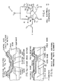
- Figure 5a illustrates in cross section a semiconductor device particularly suited for implementing the structure shown in Figure 1.
- P-type substrate typically ⁇ 100> material with a resistivity of 2-50 0-cm
- a gate oxide Formed over the surface of the active region of the device is a gate oxide and formed over the gate oxide is a floating gate of a conductive material such as doped polycrystalline silicon or molybdenum.
- dielectric typically silicon dioxide or silicon nitride
- the control gate is again formed of doped polycrystalline silicon, a silicide or selected metal such as aluminum and is capacitively coupled to the floating gate.
- the tunnelling oxide portion is formed directly over the drain such that electrons can tunnel in response to the proper voltages applied to the drain and the floating gate from one to the other.
- a control gate typically formed of doped polycrystalline silicon. This control gate is capacitively coupled to the floating gate so as to control the potential of the floating gate.
Landscapes
- Non-Volatile Memory (AREA)
- Semiconductor Memories (AREA)
Applications Claiming Priority (4)
| Application Number | Priority Date | Filing Date | Title |
|---|---|---|---|
| US06/324,344 US4435786A (en) | 1981-11-23 | 1981-11-23 | Self-refreshing memory cell |
| US324344 | 1981-11-23 | ||
| US324343 | 1981-11-23 | ||
| US06/324,343 US4423491A (en) | 1981-11-23 | 1981-11-23 | Self-refreshing memory cell |
Related Child Applications (1)
| Application Number | Title | Priority Date | Filing Date |
|---|---|---|---|
| EP88118696.9 Division-Into | 1982-11-22 |
Publications (3)
| Publication Number | Publication Date |
|---|---|
| EP0080415A2 true EP0080415A2 (de) | 1983-06-01 |
| EP0080415A3 EP0080415A3 (en) | 1985-10-09 |
| EP0080415B1 EP0080415B1 (de) | 1990-10-10 |
Family
ID=26984408
Family Applications (1)
| Application Number | Title | Priority Date | Filing Date |
|---|---|---|---|
| EP82402116A Expired EP0080415B1 (de) | 1981-11-23 | 1982-11-22 | Speicherzelle mit Selbstauffrischung |
Country Status (3)
| Country | Link |
|---|---|
| EP (1) | EP0080415B1 (de) |
| CA (1) | CA1189972A (de) |
| DE (1) | DE3280258D1 (de) |
Family Cites Families (3)
| Publication number | Priority date | Publication date | Assignee | Title |
|---|---|---|---|---|
| GB2000407B (en) * | 1977-06-27 | 1982-01-27 | Hughes Aircraft Co | Volatile/non-volatile logic latch circuit |
| GB2058451B (en) * | 1979-09-13 | 1983-03-16 | Plessey Co Ltd | Semiconductor memory device |
| GB2063601B (en) * | 1979-11-12 | 1984-02-29 | Hughes Microelectronics Ltd | Non-volatile semiconductor memory circuits |
-
1982
- 1982-11-22 CA CA000416051A patent/CA1189972A/en not_active Expired
- 1982-11-22 EP EP82402116A patent/EP0080415B1/de not_active Expired
- 1982-11-22 DE DE8282402116T patent/DE3280258D1/de not_active Expired - Fee Related
Also Published As
| Publication number | Publication date |
|---|---|
| DE3280258D1 (de) | 1990-11-15 |
| EP0080415B1 (de) | 1990-10-10 |
| EP0080415A3 (en) | 1985-10-09 |
| CA1189972A (en) | 1985-07-02 |
Similar Documents
| Publication | Publication Date | Title |
|---|---|---|
| US4435786A (en) | Self-refreshing memory cell | |
| EP0467928B1 (de) | Novramzell unter verwendung von zwei differentialen entkopplungsbaren nichtflüchtigen speicherelementen | |
| US4907198A (en) | Semiconductor memory device | |
| US6058051A (en) | Memory cell of non-volatile semiconductor memory device | |
| US5742542A (en) | Non-volatile memory cells using only positive charge to store data | |
| US4715014A (en) | Modified three transistor EEPROM cell | |
| EP0586473B1 (de) | Nicht-fluechtige loeschbare und programmierbare verbindungszelle | |
| EP0551926A1 (de) | Nichtflüchtige Halbleiter-Speicheranordnung | |
| EP0295935A1 (de) | Elektrisch löschbarer und programmierbarer Nur-Lese-Speicher | |
| EP0052566A2 (de) | Elektrisch löschbarer, programmierbarer Festwertspeicher | |
| JP2688612B2 (ja) | 不揮発性メモリ装置 | |
| US4999812A (en) | Architecture for a flash erase EEPROM memory | |
| JPS62117196A (ja) | 電気的に消去可能なプログラム可能なメモリ・セルとその製法 | |
| JPH0777078B2 (ja) | 不揮発性半導体メモリ | |
| US4479203A (en) | Electrically erasable programmable read only memory cell | |
| EP0280883B1 (de) | Halbleiter-Festwertspeichereinrichtung | |
| US5251171A (en) | Method of operating a semiconductor memory device | |
| US5181188A (en) | Semiconductor memory device | |
| EP0866466A2 (de) | Polarisierungsweise zur Spannungsreduzierung und Zuverlässigkeitsverbesserung in EEPROM-Zellen | |
| EP0387889B1 (de) | Nichtflüchtiger Halbleiterspeicher | |
| KR960012250B1 (ko) | 반도체 비휘발성 ram | |
| US4803662A (en) | EEPROM cell | |
| US6512694B2 (en) | NAND stack EEPROM with random programming capability | |
| JPH0682811B2 (ja) | 集積回路高電圧分配方法及び装置 | |
| US4423491A (en) | Self-refreshing memory cell |
Legal Events
| Date | Code | Title | Description |
|---|---|---|---|
| PUAI | Public reference made under article 153(3) epc to a published international application that has entered the european phase |
Free format text: ORIGINAL CODE: 0009012 |
|
| AK | Designated contracting states |
Designated state(s): DE FR GB IT NL |
|
| PUAL | Search report despatched |
Free format text: ORIGINAL CODE: 0009013 |
|
| AK | Designated contracting states |
Designated state(s): DE FR GB IT NL |
|
| 17P | Request for examination filed |
Effective date: 19860401 |
|
| 17Q | First examination report despatched |
Effective date: 19870820 |
|
| RAP1 | Party data changed (applicant data changed or rights of an application transferred) |
Owner name: FAIRCHILD SEMICONDUCTOR CORPORATION |
|
| GRAA | (expected) grant |
Free format text: ORIGINAL CODE: 0009210 |
|
| AK | Designated contracting states |
Kind code of ref document: B1 Designated state(s): DE FR GB IT NL |
|
| XX | Miscellaneous (additional remarks) |
Free format text: TEILANMELDUNG 88118696.9 EINGEREICHT AM 22/11/82. |
|
| ET | Fr: translation filed | ||
| ITF | It: translation for a ep patent filed | ||
| REF | Corresponds to: |
Ref document number: 3280258 Country of ref document: DE Date of ref document: 19901115 |
|
| PLBE | No opposition filed within time limit |
Free format text: ORIGINAL CODE: 0009261 |
|
| STAA | Information on the status of an ep patent application or granted ep patent |
Free format text: STATUS: NO OPPOSITION FILED WITHIN TIME LIMIT |
|
| 26N | No opposition filed | ||
| ITTA | It: last paid annual fee | ||
| PGFP | Annual fee paid to national office [announced via postgrant information from national office to epo] |
Ref country code: GB Payment date: 19941017 Year of fee payment: 13 |
|
| PGFP | Annual fee paid to national office [announced via postgrant information from national office to epo] |
Ref country code: FR Payment date: 19941114 Year of fee payment: 13 |
|
| PGFP | Annual fee paid to national office [announced via postgrant information from national office to epo] |
Ref country code: NL Payment date: 19941130 Year of fee payment: 13 |
|
| PG25 | Lapsed in a contracting state [announced via postgrant information from national office to epo] |
Ref country code: GB Effective date: 19951122 |
|
| PG25 | Lapsed in a contracting state [announced via postgrant information from national office to epo] |
Ref country code: NL Effective date: 19960601 |
|
| GBPC | Gb: european patent ceased through non-payment of renewal fee |
Effective date: 19951122 |
|
| PG25 | Lapsed in a contracting state [announced via postgrant information from national office to epo] |
Ref country code: FR Effective date: 19960731 |
|
| NLV4 | Nl: lapsed or anulled due to non-payment of the annual fee |
Effective date: 19960601 |
|
| REG | Reference to a national code |
Ref country code: FR Ref legal event code: ST |
|
| PGFP | Annual fee paid to national office [announced via postgrant information from national office to epo] |
Ref country code: DE Payment date: 19980126 Year of fee payment: 16 |
|
| PG25 | Lapsed in a contracting state [announced via postgrant information from national office to epo] |
Ref country code: DE Free format text: LAPSE BECAUSE OF NON-PAYMENT OF DUE FEES Effective date: 19990901 |