EP0078726B1 - Dispositif à transfert d'électrons fonctionnant dans le domaine des hyperfréquences - Google Patents
Dispositif à transfert d'électrons fonctionnant dans le domaine des hyperfréquences Download PDFInfo
- Publication number
- EP0078726B1 EP0078726B1 EP82401919A EP82401919A EP0078726B1 EP 0078726 B1 EP0078726 B1 EP 0078726B1 EP 82401919 A EP82401919 A EP 82401919A EP 82401919 A EP82401919 A EP 82401919A EP 0078726 B1 EP0078726 B1 EP 0078726B1
- Authority
- EP
- European Patent Office
- Prior art keywords
- layer
- cathode
- insulating
- insulating zones
- contact
- Prior art date
- Legal status (The legal status is an assumption and is not a legal conclusion. Google has not performed a legal analysis and makes no representation as to the accuracy of the status listed.)
- Expired
Links
- 239000000463 material Substances 0.000 claims description 15
- 238000001465 metallisation Methods 0.000 claims description 13
- 239000000758 substrate Substances 0.000 claims description 13
- 238000002347 injection Methods 0.000 claims description 11
- 239000007924 injection Substances 0.000 claims description 11
- 230000005684 electric field Effects 0.000 claims description 8
- 230000027756 respiratory electron transport chain Effects 0.000 claims description 8
- 239000002784 hot electron Substances 0.000 claims description 6
- 239000004065 semiconductor Substances 0.000 claims description 6
- 238000000407 epitaxy Methods 0.000 claims description 4
- 238000005468 ion implantation Methods 0.000 claims description 3
- 238000000151 deposition Methods 0.000 claims description 2
- 230000008021 deposition Effects 0.000 claims 1
- 239000010410 layer Substances 0.000 description 48
- 229910001218 Gallium arsenide Inorganic materials 0.000 description 9
- 238000009825 accumulation Methods 0.000 description 8
- 230000007935 neutral effect Effects 0.000 description 6
- 230000007246 mechanism Effects 0.000 description 5
- 230000004888 barrier function Effects 0.000 description 4
- 230000006378 damage Effects 0.000 description 4
- 230000000694 effects Effects 0.000 description 4
- 238000000034 method Methods 0.000 description 4
- 241001644893 Entandrophragma utile Species 0.000 description 3
- 230000015572 biosynthetic process Effects 0.000 description 3
- 230000007423 decrease Effects 0.000 description 3
- 239000000243 solution Substances 0.000 description 3
- 230000000903 blocking effect Effects 0.000 description 2
- 239000002131 composite material Substances 0.000 description 2
- 150000001875 compounds Chemical class 0.000 description 2
- 230000007547 defect Effects 0.000 description 2
- 238000013461 design Methods 0.000 description 2
- 238000004519 manufacturing process Methods 0.000 description 2
- 238000001451 molecular beam epitaxy Methods 0.000 description 2
- 230000010355 oscillation Effects 0.000 description 2
- 230000008261 resistance mechanism Effects 0.000 description 2
- 239000002344 surface layer Substances 0.000 description 2
- 238000012546 transfer Methods 0.000 description 2
- -1 H + Chemical class 0.000 description 1
- 238000005280 amorphization Methods 0.000 description 1
- 230000003321 amplification Effects 0.000 description 1
- 238000013459 approach Methods 0.000 description 1
- 230000008901 benefit Effects 0.000 description 1
- 239000000969 carrier Substances 0.000 description 1
- 230000015556 catabolic process Effects 0.000 description 1
- 239000013078 crystal Substances 0.000 description 1
- 238000013016 damping Methods 0.000 description 1
- 229940082150 encore Drugs 0.000 description 1
- 239000012634 fragment Substances 0.000 description 1
- 230000006872 improvement Effects 0.000 description 1
- 150000002500 ions Chemical class 0.000 description 1
- 230000001788 irregular Effects 0.000 description 1
- 230000000873 masking effect Effects 0.000 description 1
- 238000005259 measurement Methods 0.000 description 1
- 239000000203 mixture Substances 0.000 description 1
- 238000012986 modification Methods 0.000 description 1
- 230000004048 modification Effects 0.000 description 1
- 238000003199 nucleic acid amplification method Methods 0.000 description 1
- 238000000206 photolithography Methods 0.000 description 1
- 230000000704 physical effect Effects 0.000 description 1
- 238000005498 polishing Methods 0.000 description 1
- 230000001737 promoting effect Effects 0.000 description 1
- 230000001902 propagating effect Effects 0.000 description 1
- 238000000926 separation method Methods 0.000 description 1
- 230000003068 static effect Effects 0.000 description 1
- 238000005728 strengthening Methods 0.000 description 1
- 238000011144 upstream manufacturing Methods 0.000 description 1
Images
Classifications
-
- H—ELECTRICITY
- H10—SEMICONDUCTOR DEVICES; ELECTRIC SOLID-STATE DEVICES NOT OTHERWISE PROVIDED FOR
- H10N—ELECTRIC SOLID-STATE DEVICES NOT OTHERWISE PROVIDED FOR
- H10N80/00—Bulk negative-resistance effect devices
- H10N80/10—Gunn-effect devices
- H10N80/107—Gunn diodes
Definitions
- the invention relates to an electron transfer diode, and more precisely a new cathode structure for this type of diode, more commonly called the Gunn diode.
- the purpose of this new cathode is to increase the useful power of the diode, in the microwave domain.
- Gunn diodes are microwave generation or amplification components whose operation is based on a negative volume resistance mechanism, inherent in certain compounds of the III-V family, in particular GaAs and InP, among others.
- the conduction band of III-V compounds such as GaAs or InP has two valleys, sometimes three, but we will limit our to the simpler model of two valleys: the main valley in which the electrons are very mobile ( ⁇ > 5000 cm 2 N / s for a doping concentration Ni 10 15 cm- 3 ) and the secondary valley in which the mobility is approximately 20 times lower.
- the secondary minimum is located, in the energy scale, a few tenths of electron volts (0.35 ev for GaAs, 0.5 eV for InP) above the main minimum. It follows that if an electric field is applied to a GaAs bar provided with two ohmic contacts, the apparent mobility will be a function of the value of this electric field.
- a d being the differential conductivity, e the dielectric constant of the medium, the growth rate said is linked to the dielectric relaxation, which corresponds to negative damping since ⁇ d ⁇ 0, while propagating from the cathode to the anode at the average speed of the carriers. It is therefore a convective instability, the characteristics of which depend not only on the physical properties of the material, but also, very critically, on the initial conditions, that is to say the injection conditions at the cathode.
- the first solution known in particular from patent application FR-A-2031 421, seems simple, since it is a Schottky contact, but in fact, for this Schottky contact to properly limit the current, it is it must be a low barrier contact, on N + material, and the reproducibility of such contacts is poor.
- the second solution consists in inserting in the active layer of the diode a thin layer of high doping, which makes it possible to accentuate the value of the electric field in the cathode region compared to the field in the transit region, thus favoring the injection of 'hot electrons. This is a fairly elaborate structure, since the active layer of the diode is made up of three regions, and its realization is more difficult and less reproducible than a simple structure.
- the solution provided by the cathode according to the invention is on the contrary both simple to carry out, and effective in its effects. It constitutes a modification of a conventional Gunn diode, comprising on a monocrystalline N T substrate covered with an epitaxial N + buffer layer intended to smooth the surface of the substrate, an N active layer and an N + layer intended to promote the formation of '' a metallic ohmic cathode contact.
- the anode contact is made by metallization on the substrate.
- the transparency ratio of the cathode is modified by amorphization of part of the N + layer, over its entire thickness with a slight encroachment on the underlying N layer.
- the transparency ratio is modified as a function of the ratio of the crystalline surface to the total surface, and the amorphized part is in the form of bands or studs arranged in a grid, obtained by bombardment of protons.
- the invention consists of an electron transfer device constituting a diode, operating in the microwave domain, the semiconductor body of which comprises, deposited on a monocrystalline substrate covered with an epitaxial buffer layer, a first layer active and a second layer deposited on the active layer, as well as two metallizations, the first for the anodic contact on the substrate and the second for the cathodic contact on the second layer, this device being characterized in that the body is in a semiconductor material of group III-V , the substrate, the buffer layer and the second layer being N + doped, and the first active layer being N doped, and in that, with a view to limiting the current and strengthening the electric field in the region of the cathodic contact, under cathode metallization are carried out in the second layer of amorphized insulating zones, in order to modify the transparency ratio of the cathode, this being the ratio between the conductive crystal surface and the total surface, at the cathode metallization.
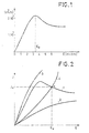
- the field being expressed in kilovolts per centimeter, we see on this curve that the speed of the electrons, in centimeters per second, passes through a maximum located around 3500 V / cm for GaAs.
- the electrons are in the main valley of the conduction band, they are very mobile.
- the electrons are in the secondary valley of the conduction band and they are less mobile.
- the region of the curve in which the speed decreases when the field increases has a negative resistance in volume: this is the operating range of electron transfer diodes.
- Figure 1 relates to a type of ohmic contact, which is said to be injecting. There are other types of cathode contacts.
- FIG. 2 represents the characteristics of a cathodic contact, and gives the different curves of current density J as a function of the field E, for the injecting contacts, and the limiting contacts.
- curve marked 1 corresponds to a neutral characteristic.
- Curve 2 such that it does not intersect and is less than curve 1 of neutral characteristic for any value of the field, leads to a limiting limiting contact.
- curve 3 is ordinarily always greater than curve 1; whatever the field: it corresponds to an injecting contact.
- curve 4 intersects curve 1 at a point X corresponding to a field E x : if the field E> E x , the contact is. injecting and if E ⁇ E x the contact is limiting.
- the Schottky contact uses a very low barrier of 0.15 to 0.25 eV.
- the disadvantage of this contact is that if the injection is made by thermionic emission, it is very sensitive to temperature, which is inconvenient for components used in military and space equipment. This situation can be remedied by using a Schottky contact on N + material, which gives a tunnel injection not very sensitive to temperature, but risks on the other hand leading to an insufficient current limitation. In addition, the reproducibility of low barrier Schottky contacts is poor.
- the cathode with one or two zones: it is a low barrier ohmic or Schottky contact, on an N- doped region, followed by a second region, not very thick but very doped.
- the first region leads to a current limitation
- the doping peak of the second region makes it possible to accentuate the value of the field in the cathode region relative to the field in the transit region, thus promoting the injection of hot electrons.
- This type of cathode has been tested on InP, where the dead zone is more extensive than in the case of GaAs. It allows operating conditions much less sensitive to temperature than the Schottky contact while offering a current limitation. However, it is a very elaborate structure whose realization is difficult and probably not very reproducible.
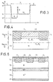
- FIG. 3 represents the concentration profile of such a known diode, with several zones.
- the doping concentration N d being plotted on the ordinate, the abscissas represent distances: there is thus a cross section of a diode, the cathode being region 5; the anode region 6 and the different layers of the diode in the central part 7.
- region region 8 is that which, doped N-, leads to a current limitation, and region 9, by its peak doping, accentuates the field in region 8, suppresses dissipative functioning, and injects hot electrons into the active layer 10 of the diode.
- the representation of the doping levels in regions 5 and 6 corresponds to the N + layers located under the contact, cathode and anode metallizations.
- FIG. 4 shows a fragment of the cathode according to the invention, and will explain the mechanism of the invention. This FIG. 4 is limited to the first two layers of the diode: those which are not necessary for understanding are not shown.
- the cathode structure comprises, starting from the metallization 11 of contact making, a layer 12 of N + doping and a layer 13 of N doping.
- Amorphized insulating zones 14, produced by techniques which will be described later, are delimited on the surface of the cathode, so as to reduce the section offered to the current: the ratio of the remaining crystalline surface of the layer 12 to the total surface of the cathodic contact is called the transparency ratio.
- the thickness of the insulating zones 14 slightly exceeds that of the N + layer 12, which is of the order of 0.5 ⁇ to 1 ⁇ .
- the field of the invention belongs to cases where the thickness of the insulating zones is equal to or less than the thickness of the N + 12 layer.
- the space of the diode is thus divided into two regions, region 1 in which the section offered to the current is Si, and region II of section S 2 larger.
- Ci and C 2 be two planes close and located on either side of the plane of separation of regions I and II: they therefore have sections Si and S 2 respectively.
- This structure has injection characteristics comparable to those of the two-zone cathode.
- E 1 , I 1 and E 2 , 1 2 be the fields and the currents in the planes Ci and C 2 .
- Current continuity requires:
- the plane Ci being placed slightly beyond the layer N + and the contact N + being injecting, we have in C 1 : n> N d .
- the ratio of the sections S 2 / S 1 is chosen large enough so that at the level of the plane C 2 there is current limitation, therefore n ⁇ N d .
- this mechanism is only valid for a given current, but a Gunn diode operates with a practically fixed bias current.
- FIG. 5 represents a sectional view of an electron transfer diode provided with a cathode according to the invention.
- the basic structure is conventional: on a substrate 16, monocrystalline, N + , in GaAs or InP or any other material of the same kind, of group III-V, is deposited a buffer layer 15, epitaxial, of N + type and same material as the substrate 16.
- the function of the buffer layer 15 is to attenuate surface defects of the substrate, such as polishing scratches.
- an active layer 13, of type N is epitaxied on the buffer layer 15, and finally a surface layer 12, of type N + , the latter two layers also being in GaAs or InP.
- Two contact metallizations complete the diode, a metallization 17 on the substrate for the anode, and a metallization 11 for the cathode.
- part of the surface layer 12 and the part of the active layer 13 located opposite are amorphized in such a way that the amorphized insulating zones 14 thus formed penetrate into the active layer 13.
- the amorphous zones 14 can be of geometries such as bands, parallel or not, rings, concentric or not, or studs arranged in grid or checkerboard: the important thing is to modify the transparency ratio of the cathode, in order to limit the current in this cathode region, and to strengthen the field to produce hot electrons.
- a strip or pad 14 has a width of 0.7 ⁇ .
- the insulating zones 14 can be produced by different techniques including ion implantation or epitaxial growth by molecular jets on amorphous surfaces.
- the ion implantation technique consists in amorphizing the semiconductor material, by implanting protons or ions such as H + , 0 + , etc. at 80 keV and 4.10 14 coulombs / cm 2 .
- the boundaries of the implanted areas are made by photolithography.
- the N + substrate structure - N + buffer - active layer N is first produced. Then a thin layer of amorphous material such as Si0 2 is deposited on the appropriate parts, or the surface of the semiconductor is slightly oxidized. The N + 13 and N + 12 layers necessary for the complete constitution of the diode structure are then deposited by molecular beam epitaxy. On the parts where the amorphous material exists, the deposit is irregular and insulating, while elsewhere the layers have the desired N or N + properties .
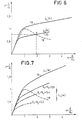
- Curve 18 represents the neutral characteristic, curve 19 the cathode characteristic j C1 (e) and curve 20 the cathode characteristic J C2 (e).
Landscapes
- Electrodes Of Semiconductors (AREA)
- Input Circuits Of Receivers And Coupling Of Receivers And Audio Equipment (AREA)
- Details Of Aerials (AREA)
Applications Claiming Priority (2)
| Application Number | Priority Date | Filing Date | Title |
|---|---|---|---|
| FR8120444A FR2515866A1 (fr) | 1981-10-30 | 1981-10-30 | Dispositif a transfert d'electrons fonctionnant le domaine des hyperfrequences |
| FR8120444 | 1981-10-30 |
Publications (2)
| Publication Number | Publication Date |
|---|---|
| EP0078726A1 EP0078726A1 (fr) | 1983-05-11 |
| EP0078726B1 true EP0078726B1 (fr) | 1985-08-28 |
Family
ID=9263581
Family Applications (1)
| Application Number | Title | Priority Date | Filing Date |
|---|---|---|---|
| EP82401919A Expired EP0078726B1 (fr) | 1981-10-30 | 1982-10-19 | Dispositif à transfert d'électrons fonctionnant dans le domaine des hyperfréquences |
Country Status (4)
| Country | Link |
|---|---|
| EP (1) | EP0078726B1 (enExample) |
| JP (1) | JPS5884480A (enExample) |
| DE (1) | DE3265875D1 (enExample) |
| FR (1) | FR2515866A1 (enExample) |
Families Citing this family (1)
| Publication number | Priority date | Publication date | Assignee | Title |
|---|---|---|---|---|
| FR2519473A1 (fr) * | 1981-12-31 | 1983-07-08 | Thomson Csf | Dispositif unipolaire a transfert d'electrons du type diode gunn |
Family Cites Families (3)
| Publication number | Priority date | Publication date | Assignee | Title |
|---|---|---|---|---|
| GB1266154A (enExample) * | 1968-07-02 | 1972-03-08 | ||
| NL6902447A (enExample) * | 1969-02-14 | 1970-08-18 | ||
| FR2293068A1 (fr) * | 1974-11-29 | 1976-06-25 | Thomson Csf | Dispositif semi-conducteur a effet gunn |
-
1981
- 1981-10-30 FR FR8120444A patent/FR2515866A1/fr active Granted
-
1982
- 1982-10-19 DE DE8282401919T patent/DE3265875D1/de not_active Expired
- 1982-10-19 EP EP82401919A patent/EP0078726B1/fr not_active Expired
- 1982-10-28 JP JP57189953A patent/JPS5884480A/ja active Pending
Also Published As
| Publication number | Publication date |
|---|---|
| FR2515866A1 (fr) | 1983-05-06 |
| DE3265875D1 (en) | 1985-10-03 |
| JPS5884480A (ja) | 1983-05-20 |
| FR2515866B1 (enExample) | 1983-12-02 |
| EP0078726A1 (fr) | 1983-05-11 |
Similar Documents
| Publication | Publication Date | Title |
|---|---|---|
| EP0881690B1 (fr) | Procédé de réalisation d'un transistor bipolaire stabilisé avec éléments isolants électriques | |
| EP3203526B1 (fr) | Transistor à hétérojonction à confinement de gaz d'électrons amélioré | |
| EP3012876B1 (fr) | Procede de fabrication d'une photodiode a faible bruit | |
| EP0006983B1 (fr) | Transistor à tension d'avalanche commandée pouvant être sensible à un champ magnétique | |
| WO2001048829A1 (fr) | Transistor bipolaire a heterojonction a collecteur en haut et procede de realisation | |
| FR2568410A1 (fr) | Transistor statique a induction et son circuit integre | |
| FR2508707A1 (fr) | Transistor balistique a multiples heterojonctions | |
| FR2463511A1 (fr) | Transistor a porteurs de charge chauds | |
| FR2468208A1 (fr) | Dispositif semiconducteur avec une diode zener | |
| FR2819342A1 (fr) | Transistor bipolaire a heterojonction, a auto-alignement, et son procede de realisation | |
| EP0078726B1 (fr) | Dispositif à transfert d'électrons fonctionnant dans le domaine des hyperfréquences | |
| FR2496990A1 (fr) | Transistor a effet de champ a barriere schottky | |
| EP0083531B1 (fr) | Dispositif unipolaire à transfert d'électrons du type diode gunn | |
| FR2569056A1 (fr) | Transistor a induction statique du type a injection par effet tunnel et circuit integre comprenant un tel transistor | |
| US4038106A (en) | Four-layer trapatt diode and method for making same | |
| EP4088312B1 (fr) | Procédé de fabrication d'une structure de type semi-conducteur sur isolant pour applications radiofréquences | |
| EP0197838A1 (fr) | Procédé de réalisation d'un transistor à effet de champ à métallisation de grille autoalignée | |
| FR2721439A1 (fr) | Eléments semi-conducteurs optiques et procédés de fabrication de ceux-ci. | |
| FR2601507A1 (fr) | Diode a transfert d'electrons, a regions balistiques periodiques | |
| FR2554639A1 (fr) | Transistor a effet de champ a tension de seuil reglable, et circuit integre comportant ce type de transistors | |
| RU2805001C1 (ru) | Конструкция поверхностного ТГц излучателя | |
| EP2735016A1 (fr) | Dispositif semi-conducteur d'emission d'electrons dans le vide | |
| WO2004102602A1 (fr) | Dispositif semi-conducteur d'emission d'electrons dans le vide | |
| FR3155957A1 (fr) | Substrat semi-conducteur sur isolant optimisé pour des basses températures | |
| EP0030178A2 (fr) | Transistor à effet de champ et procédé de fabrication de celui-ci |
Legal Events
| Date | Code | Title | Description |
|---|---|---|---|
| PUAI | Public reference made under article 153(3) epc to a published international application that has entered the european phase |
Free format text: ORIGINAL CODE: 0009012 |
|
| AK | Designated contracting states |
Designated state(s): DE GB IT NL |
|
| 17P | Request for examination filed |
Effective date: 19830526 |
|
| ITF | It: translation for a ep patent filed | ||
| GRAA | (expected) grant |
Free format text: ORIGINAL CODE: 0009210 |
|
| AK | Designated contracting states |
Designated state(s): DE GB IT NL |
|
| REF | Corresponds to: |
Ref document number: 3265875 Country of ref document: DE Date of ref document: 19851003 |
|
| PLBE | No opposition filed within time limit |
Free format text: ORIGINAL CODE: 0009261 |
|
| STAA | Information on the status of an ep patent application or granted ep patent |
Free format text: STATUS: NO OPPOSITION FILED WITHIN TIME LIMIT |
|
| 26N | No opposition filed | ||
| ITTA | It: last paid annual fee | ||
| PGFP | Annual fee paid to national office [announced via postgrant information from national office to epo] |
Ref country code: DE Payment date: 19950923 Year of fee payment: 14 |
|
| PGFP | Annual fee paid to national office [announced via postgrant information from national office to epo] |
Ref country code: GB Payment date: 19960918 Year of fee payment: 15 |
|
| PGFP | Annual fee paid to national office [announced via postgrant information from national office to epo] |
Ref country code: NL Payment date: 19960926 Year of fee payment: 15 |
|
| PG25 | Lapsed in a contracting state [announced via postgrant information from national office to epo] |
Ref country code: DE Effective date: 19961004 |
|
| PG25 | Lapsed in a contracting state [announced via postgrant information from national office to epo] |
Ref country code: GB Free format text: LAPSE BECAUSE OF NON-PAYMENT OF DUE FEES Effective date: 19971019 |
|
| PG25 | Lapsed in a contracting state [announced via postgrant information from national office to epo] |
Ref country code: NL Free format text: LAPSE BECAUSE OF NON-PAYMENT OF DUE FEES Effective date: 19980501 |
|
| GBPC | Gb: european patent ceased through non-payment of renewal fee |
Effective date: 19971019 |
|
| NLV4 | Nl: lapsed or anulled due to non-payment of the annual fee |
Effective date: 19980501 |