EP0077657A2 - Apparatus and methodology for configuration of an input/output digital circuit among different input/output protocols - Google Patents
Apparatus and methodology for configuration of an input/output digital circuit among different input/output protocols Download PDFInfo
- Publication number
- EP0077657A2 EP0077657A2 EP82305495A EP82305495A EP0077657A2 EP 0077657 A2 EP0077657 A2 EP 0077657A2 EP 82305495 A EP82305495 A EP 82305495A EP 82305495 A EP82305495 A EP 82305495A EP 0077657 A2 EP0077657 A2 EP 0077657A2
- Authority
- EP
- European Patent Office
- Prior art keywords
- circuit
- user
- input
- protocol
- receiver
- Prior art date
- Legal status (The legal status is an assumption and is not a legal conclusion. Google has not performed a legal analysis and makes no representation as to the accuracy of the status listed.)
- Withdrawn
Links
- 238000000034 method Methods 0.000 title claims description 11
- 239000000872 buffer Substances 0.000 claims abstract description 48
- 238000004891 communication Methods 0.000 claims description 86
- 230000006872 improvement Effects 0.000 claims description 21
- 230000008878 coupling Effects 0.000 claims description 17
- 238000010168 coupling process Methods 0.000 claims description 17
- 238000005859 coupling reaction Methods 0.000 claims description 17
- 230000013011 mating Effects 0.000 claims description 4
- 230000009977 dual effect Effects 0.000 claims description 2
- 230000000694 effects Effects 0.000 claims description 2
- 230000002093 peripheral effect Effects 0.000 description 14
- 230000000875 corresponding effect Effects 0.000 description 5
- 238000010586 diagram Methods 0.000 description 3
- 238000013519 translation Methods 0.000 description 3
- 101001122938 Homo sapiens Lysosomal protective protein Proteins 0.000 description 2
- 102100028524 Lysosomal protective protein Human genes 0.000 description 2
- 230000008901 benefit Effects 0.000 description 2
- 230000008521 reorganization Effects 0.000 description 2
- RYGMFSIKBFXOCR-UHFFFAOYSA-N Copper Chemical compound [Cu] RYGMFSIKBFXOCR-UHFFFAOYSA-N 0.000 description 1
- 230000006978 adaptation Effects 0.000 description 1
- 230000004075 alteration Effects 0.000 description 1
- 230000008859 change Effects 0.000 description 1
- 238000012512 characterization method Methods 0.000 description 1
- 239000004020 conductor Substances 0.000 description 1
- 238000010276 construction Methods 0.000 description 1
- 230000002079 cooperative effect Effects 0.000 description 1
- 229910052802 copper Inorganic materials 0.000 description 1
- 239000010949 copper Substances 0.000 description 1
- 230000006870 function Effects 0.000 description 1
- 238000003780 insertion Methods 0.000 description 1
- 230000037431 insertion Effects 0.000 description 1
- 239000000463 material Substances 0.000 description 1
- 238000012986 modification Methods 0.000 description 1
- 230000004048 modification Effects 0.000 description 1
- 230000004044 response Effects 0.000 description 1
- 230000001360 synchronised effect Effects 0.000 description 1
Images


Classifications
-
- G—PHYSICS
- G06—COMPUTING; CALCULATING OR COUNTING
- G06F—ELECTRIC DIGITAL DATA PROCESSING
- G06F13/00—Interconnection of, or transfer of information or other signals between, memories, input/output devices or central processing units
- G06F13/38—Information transfer, e.g. on bus
- G06F13/382—Information transfer, e.g. on bus using universal interface adapter
- G06F13/385—Information transfer, e.g. on bus using universal interface adapter for adaptation of a particular data processing system to different peripheral devices
Definitions
- the present invention relates to the field of interfacing communication channels and in particular, it relates to an improved method and circuitry for interfacing users communicating according to different protocols on a communication channel.
- a computer operating system typically includes a number of internal busses and a variety of peripheral devices through which the system is used. It is not uncommon for peripherals to communicate with the computer operating system over a local input/output bus. This means, of course, that each of the peripherals and other elements within the computer operating system must be able to communicate according to the same protocol. Protocol is defined here to refer to the unique characterization of signals according to their significance, voltage levels, timing and number.
- peripheral communication channels specially configured to communicate between their local input/output bus and such peripherals.
- Each such specially configured communication channel includes circuitry that translates communications between the protocol used on the local input/output bus and that used by the interfaced peripheral.
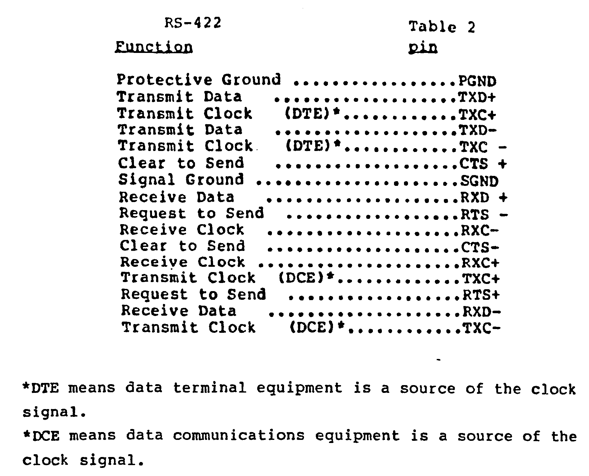
- Two such standards are known as RS-232 and R S-422.
- the preferred embodiment of the present invention described hereinafter with reference to the drawings is arranged to provide selective communication according to these two standards.
- Prior art interface circuitry has been designed to translate communications between one local input/output bus protocol and only one peripheral input/output protocol. Consequently, to communicate between a computer system and different peripherals operating according to different communication protocols, it has been the practice to provide a separate and dedicated peripheral communication channel for each different protocol.
- the present invention is an improved method and circuitry for communicating a communication channel and a user according to a protocol selected from a plurality of different permissible protocols.
- the improved method of the present invention comprises the step of selectively configuring an interface circuit in one of different selectable circuit configurations to execute communications between the communication channel and users according to a selected permissible protocol. For users operating according to a different permissible user protocol, the configuration of the interface circuit is selectively changed to execute communications according to the different permissible protocol.
- the improved circuitry of the present invention comprises an interface circuit selectively configurable for interfacing the communication channel for communication with users operating according to different permissible protocols.
- a switching means is coupled to the interface circuit and is selectively operable to configure such circuit for communicating the communication channel with users according to a selected one of the permissible user protocols.
- the improved interface circuitry of the present invention enables the construction of multi-channel communication systems capable of communicating with users operating according to different combinations of protocols. More particularly, one embodiment of the improved interface circuitry comprises first and at least second channels of communication, at least one of which is interfaced to users operating according to different communication protocols.
- a first interface circuit is coupled to the first channel to communicate with a user according to a first protocol.
- a second interface circuit is coupled to the second channel and is selectably configurable to communicate with a user according to a protocol selected from either the first or at least a second permissible protocol.
- Switching means is provided for selectively configuring the second interface circuit to communicate with the user according to a selected one of the permissible protocols.
- a dual channel interface circuit has at least one channel of communication which is switchable or otherwise arbitrarily configurable in different protocol translation modes, whereby the two communication channels are capable of communicating with users operating according to different selected combinations of protocols.
- the improved circuitry of the present invention is particularly useful for communicating a computer operating system and a user.
- the computer operating system is coupled to an input/output bus and an input/output interface circuit is coupled to the bus for communicating it to the user.
- the input/output interface circuit is coupled to a first receiver means for receiving user compatible signals communicated by a user according to a first protocol and couple corresponding signals to the input/output interface circuit compatible with the protocol of such circuit.
- a first transmitter means is coupled to receive signals from the input/output interface circuit communicated according to protocol of such circuit and transmit user compatible signals to the user according to the first protocol.
- a second receiver means is coupled to receiving user compatible signals communicated by a user according to'a second protocol and couple corresponding signals to the input/output interface circuit compatible with the protocol of such circuit.
- a second transmitter means is coupled to receive signals from the input/outpct interface circuit communicated according to the protocol of such circuit and transmit user compatible signals according to the second protocol.
- Switching means is operatively associated with the receiver and transmitter means for selectively coupling the first receiving and transmitting means and the second receiving and transmitting means between the input/output interface circuit and the user.
- the improved interface method of the present invention is practiced conveniently by communication receiver and transmitter circuits coupled between the communication channel and a user. More particularly, such embodiment of the improved method comprises the steps of selectively switching communication from a user to a communication channel through first and second receiver buffer circuits, which are adapted to receive communications from users according to first and second protocols, respectively. Both first and second receiver buffer circuits are adapted to couple communications to the channel according to the protocol of the channel. In another step, communication from the channel to the user is selectively switched through first and second transmitter buffer circuits, which are adapted to transmit communications to the user in the first and second protocols, respectively. Both first and second transmitter buffer circuits are adapted to receive communications from the channel in the protocol of the channel and transmit corresponding communications in their respective transmitting protocols.
- the present invention is an improvement in interfacing communications wherein the translation between a local communication channel protocol and an external user protocol can be selectively controlled.
- the improvement includes circuitry and a method by which the configuration of an interface circuit coupled between the communication channel and the external user can be selectively and readily changed to allow the communication channel to communicate with the external user in a selected one of different protocols.
- the present invention includes applications where two or more protocols may be selected.
- the change in configuration of the interface circuit is accomplished by switching communication between the communication channel and the user through different ones of two separate sets of buffer circuits, each of which is adapted to translate communications between the communication protocol of the communication channel and one of the user protocols.
- the latter reconfiguration is employed in the preferred embodiment solely for the purpose of convenience of adaptation of the present invention to the RS-232 and RS-422 protocols employed in the preferred embodiment of the invention.
- Other groups of protocols may be included now or in the future which would allow reconfiguration of the interface circuit by means of reorganization within a given set of buffer circuits.
- Computer operating system 10 contains a large number of differing elements such as a general purpose central processor, internal clocks, dedicated and special purpose central processors, various types of memory, direct memory addressing logic, video control circuitry and so forth.
- Computer operating system 10 is coupled to a local input/output bus 12 which is illustrated as being of byte width.
- Input/output bus 12 may in turn be coupled to a large number of -peripherals which are compatible with the input/output protocol used on bus 12.
- Such peripherals may include a keyboard interface. '
- bus 12 is coupled to a serial input/output (S10) communications control circuit 14.
- S10 communications control circuit 14 has at least two channels, channel A and channel B, for communication with external peripherals.
- Channel B is capable of compatible interface operation only in one protocol, which in the preferred embodiment is the RS-232 protocol, such operation hereinafter referred to as the RS-232 mode.
- channel A is capable of being selected to operate in one of at least two protocols, which in the preferred embodiment are either the RE-232 or R S-422 compatible protocols or modes.
- the RS-232 mode is characterized by a 14 pin input/output while the RS-422 mode is characterized by a different 16 pin input/output.
- a single 16- pin terminal device indicated generally in Figures 2 and 3 by reference number 11, is employed for coupling R-232 and R-422 users to channel A. For RS-232 users, two pins are not used.
- Figure 2 shows the circuit configuration and input/outputs in the RS-232 mode
- Figure 3 shows the circuit configuration and input/outputs in the RS-422 mode.
- Circuit 14 is primarily based on a serial input/output chip, a conventional and well-known integrated circuit 16 sold as a serial input/output communications (S10) chip, type Z80A-S10. Circuit 16 is operatively associated with a 16-bit register 18 to provide two input/output channels, channel A and channel B. In the preferred embodiment of the present invention, the S10 chip of circuit 16 is operatively associated with the 16-bit register 18 so that the S10 communication control circuit 14 communicates with both,channels A and B in the same protocol. Register 18 is a conventional register sold as type 74LS 244.
- channel A has the greatest flexibility.
- Channel A includes interface circuitry indicated generally by reference number 15 that enables channel A to operate in either an RS -232 or an RS-422 mode, which channel can be controlled for communications purposes by either.a CPU or local DMA within computer operating system 12.
- DMA transfers the communication channel, channel A or B, operates only in half duplex mode since only one DMA channel is allocated to communcation and circuit 16 has only one ready line per channel for use as a DMA request signal.
- the RS-422 mode differs from the RS-232 mode primarily on the basis that RS-422 is a balanced- differential interface with an ability to transmit clocks on signals that are separate from the data.
- S10 control circuit 14 can be better understood if the signals comprising the RS-232 and RS-422 modes are first listed and defined.
- Table 1 lists the signals which comprise the RS-232 mode together with their acronyms as appear in Figures 2 and 3.
- Table 2 lists and defines the RS-422 signals.
- channel B of the operatively associated S10 circuit 16 and register 18 communicates directly with interface circuitry indicated generally by reference number 19 comprising a plurality of buffer circuits 20, 22, and 24.
- buffer circuits 20- 24 are conventional circuits which in the case of buffers 2 0 and 24 are receiver buffer circuits sold as type 1489 and in the case of buffer 22 is a transmitter buffer circuit sold as type 1488.
- the signals coupled through channel B, by means of buffer circuits 20-24, are derived by the cooperative action S10 circuit 16 and register 18 in response to the input/output bus and various control inputs shown on the top, bottom and left side of Figures 2 and 3.
- interface circuitry 15 includes buffer circuitry for communicating according to the RS-422 protocol comprising transmitter buffer circuit 26 and receiver buffer circuit 28.
- interface circuitry 15 includes RS-232 buffer circuitry comprised of transmitter buffer circuit 30 and receiver buffer circuits 32 and 34.
- Switches 36 and 38 are comprised of dual-in-line packages proviaing connections through mating plugs and sockets and in which opposite pins are strapped together by a copper bus or conductor.
- Such jumper plugs are well-known to the art.
- the buffer circuitry of channel A can be configured by means of manually removing the jumper plugs from switches or sockets 40 and 42 and inserting the plugs in switches or sockets 36 and 38. According to the present invention, removal of the plugs from switches 40 and 42 disconnects the RS-232 buffer circuitry and insertion of the plugs in switches 36 and 38 connects the RS-422 buffer circuitry.
- the circuitry and method of the present invention can be better understood by considering in detail the coupling of the RS-232 mode input and output lines of the terminal device 11 through the switching assembly to channel A of S10 circuit 16 and register 18.
- the RS-232 lines, other than protected and signal grounds, as listed in Table 1 are shown on the right hand edge of Figure 2 beginning at the top with the transmit clock signal for channel A, TXCA+ and ending-in the bottom with the ring indicator for channel A, RING A+.
- the jumper plugs are inserted in switches 40 and 42.
- Each of the four R S-232 input lines in the upper part of Figure 2, namely TXCA+, RXCA+, CTSA+ and RXDA- are coupled through switch 40 to the input of receiver 32, which is a conventional buffer circuit sold as type 1489.
- the outputs of receiver 32 are then coupled back through switch 40 at those points indicated by the arrows entirely included within the rectangle representing switch 40.
- Each of the outputs from receiver 32 are then coupled to the corresponding inputs as labeled at the channel A input ports of S10 circuit 16.
- the input lines DSRA+, SRDA+, RING A+, and DCDA+ are coupled as inputs through switch 42 to the inputs of receiver 34, also a conventional buffer circuit sold as type 1489.
- the outputs of receiver 34 are then appropriately coupled to register 18 in the case of RING A+, DSRA+ and SRDA+ and to the appropriate channel A input of S10 circuit 16 in the case of DCDA+.
- Transmitter 30 whose inputs are derived from the outputs DTRA-, RTSA-, TXDA+ of channel A of S10 circuit 16 and from random logic ultimately coupled to the input/output bus, has its outputs coupled through switch 42 to the corresponding RS-232 output lines listed on the right side of Figure 2.
- switches 40 and 42 serve two functions; they select the proper receivers and transmitters for coupling the terminal device 11 to the appropriate points within the S10 circuit 14, and they also isolate all receivers and transmitters from the terminal device 11, except those used in the selected protocol operating mode.
- the jumper plug of the switch 42 is removed to isolate the outputs of the transmitter 30 and inputs of receiver 34 from the terminal device 11.
- Switch 40 has its jumper plug removed to isolate the inputs of the receiver 32 from the terminal device 11, as well.
- the outputs of the receiver 32 are coupled to the same points within the S10 circuit 14 as certain outputs of the receiver 28 used in the RS-422 mode. For this reason, the outputs of the receiver 32 are advantageous couple to the S10 circuit 14 through the switch 40 so that they are isolated from the terminal device 11 when the apparatus is in the RS-422 mode of operation. In this manner, the receivers and transmitters used in the RS -232 operating mode are isolated from the incompatible and potentially harmful voltage and current levels of signals present on the lines of the terminal device 11 when channel A of the apparatus is in the RS-422 mode of operation.
- Figure 3 illustrates the same interface circuitry 15 of Figure 2, but connected to operate in the RS-422 mode of operation.
- Figures 2 and 3 differ principally in the direction of arrows associated with the switches 36-42 signifying the direction of communication through the interface circuitry 15 and acronyms which have been attributed to the input/output lines appearing on the right edge of Figure 3 as compared to those appearing on the right edge of Figure 2.
- a different significance is attributed to each of the input and output lines as a result of the switching executed by the switching assembly, principally switches 36 and 38.
- the removal of the plug from switch 36 isolates the inputs and outputs of the upper half of the receiver 28 from the terminal device 11 to protect that receiver from the incompatible and potentially harmful voltage and current levels of signals present on the lines of the terminal device 11 when channel A of the apparatus is placed in the RS-232 mode of operation in favor of the RS-232 mode of operation.
- the input lines CTSA+, CTSSA-, RXDA-and RXDA+ are coupled through the upper half of switch 38 to four matched inputs in the lower half of receiver 28.
- the outputs carrying the clear-to-send signal and the read-data signal are coupled through switch 36, indicated by arrows totally contained within the rectangle defining switch 36, to the received date, RXDA+, and clear-to-send and C TSA - inputs of the channel A port of circuit 16. Removal of the plugs from switches 36 and 38 protectively isolates the inputs and outputs of the lower half of the receiver 28 as described hereinbefore with reference to the upper half of the receiver 28.
- differential transmitter 26 on lines TXCA-, TXDA+, and RTSA- are derived from the appropriate channel A outputs of circuits 16 and are coupled through a conventional transmitter circuit sold as type 26 L S31.
- the differential outputs of transmitter 26 include the transmit clock signals, TXCA+ and TXCA-, which are coupled by correspondingly labeled output lines extending from transmitting 26 to the terminal 11.
- the other two pair of differential outputs or four outputs of transmitter 26 are coupled through the lower half of switch 38 and appear at lines RTSA-, RTSA+, TXDA-, TXDA+ at the middle of the right hand edge of Figure 3, on which the remaining active portions of the RS-422 mode signals appear as summarized in Table 2. Removal of the plug from switch 38 protectively isolates the outputs of the transmitter 26 from the potentially harmful current and voltage levels present on the lines of the terminal device 11 when channel A of the apparatus is in the RS-232 mode of operation.
Landscapes
- Engineering & Computer Science (AREA)
- Theoretical Computer Science (AREA)
- Physics & Mathematics (AREA)
- General Engineering & Computer Science (AREA)
- General Physics & Mathematics (AREA)
- Communication Control (AREA)
- Bus Control (AREA)
- Computer And Data Communications (AREA)
Abstract
Description
- The present invention relates to the field of interfacing communication channels and in particular, it relates to an improved method and circuitry for interfacing users communicating according to different protocols on a communication channel.
- A computer operating system typically includes a number of internal busses and a variety of peripheral devices through which the system is used. It is not uncommon for peripherals to communicate with the computer operating system over a local input/output bus. This means, of course, that each of the peripherals and other elements within the computer operating system must be able to communicate according to the same protocol. Protocol is defined here to refer to the unique characterization of signals according to their significance, voltage levels, timing and number.
- In order to communicate with peripherals which do not operate according to the same protocol as that used on the local input/output bus, prior art computer systems have used dedicated peripheral communication channels specially configured to communicate between their local input/output bus and such peripherals. Each such specially configured communication channel includes circuitry that translates communications between the protocol used on the local input/output bus and that used by the interfaced peripheral. In fact, there has arisen in the prior art well-recognized and established standards for input/output protocols used by such peripherals. Two such standards are known as RS-232 and RS-422. The preferred embodiment of the present invention described hereinafter with reference to the drawings is arranged to provide selective communication according to these two standards.
- Prior art interface circuitry, however, has been designed to translate communications between one local input/output bus protocol and only one peripheral input/output protocol. Consequently, to communicate between a computer system and different peripherals operating according to different communication protocols, it has been the practice to provide a separate and dedicated peripheral communication channel for each different protocol.
- What is needed then is a circuit and method for selectively changing the translation between a local communication channel protocol and an exterior user-protocol.
- The present invention is an improved method and circuitry for communicating a communication channel and a user according to a protocol selected from a plurality of different permissible protocols. The improved method of the present invention comprises the step of selectively configuring an interface circuit in one of different selectable circuit configurations to execute communications between the communication channel and users according to a selected permissible protocol. For users operating according to a different permissible user protocol, the configuration of the interface circuit is selectively changed to execute communications according to the different permissible protocol. By virtue of this improved method for interfacing a communication channel and its users, a single communication channel operating according to a single communication protocol can be selectively communicated with different users operating according to different communication protocols.
- The improved circuitry of the present invention comprises an interface circuit selectively configurable for interfacing the communication channel for communication with users operating according to different permissible protocols. A switching means is coupled to the interface circuit and is selectively operable to configure such circuit for communicating the communication channel with users according to a selected one of the permissible user protocols. By virtue of the improved circuitry for interfacing a communication channel and its users, a single selectively configurable interface circuit provides communication between a communication channel operating according to a single communication protocol and users operating according to different communication protocols.
- The improved interface circuitry of the present invention enables the construction of multi-channel communication systems capable of communicating with users operating according to different combinations of protocols. More particularly, one embodiment of the improved interface circuitry comprises first and at least second channels of communication, at least one of which is interfaced to users operating according to different communication protocols. A first interface circuit is coupled to the first channel to communicate with a user according to a first protocol. A second interface circuit is coupled to the second channel and is selectably configurable to communicate with a user according to a protocol selected from either the first or at least a second permissible protocol. Switching means is provided for selectively configuring the second interface circuit to communicate with the user according to a selected one of the permissible protocols. By this combination of elements, a dual channel interface circuit has at least one channel of communication which is switchable or otherwise arbitrarily configurable in different protocol translation modes, whereby the two communication channels are capable of communicating with users operating according to different selected combinations of protocols.
- The improved circuitry of the present invention is particularly useful for communicating a computer operating system and a user. The computer operating system is coupled to an input/output bus and an input/output interface circuit is coupled to the bus for communicating it to the user. The input/output interface circuit is coupled to a first receiver means for receiving user compatible signals communicated by a user according to a first protocol and couple corresponding signals to the input/output interface circuit compatible with the protocol of such circuit. A first transmitter means is coupled to receive signals from the input/output interface circuit communicated according to protocol of such circuit and transmit user compatible signals to the user according to the first protocol. A second receiver means is coupled to receiving user compatible signals communicated by a user according to'a second protocol and couple corresponding signals to the input/output interface circuit compatible with the protocol of such circuit. A second transmitter means is coupled to receive signals from the input/outpct interface circuit communicated according to the protocol of such circuit and transmit user compatible signals according to the second protocol. Switching means is operatively associated with the receiver and transmitter means for selectively coupling the first receiving and transmitting means and the second receiving and transmitting means between the input/output interface circuit and the user. By virtue of this combination of elements, the computer operating system can communicate with users through the input/output interface circuit in a protocol arbitrarily selected from the first and second protocols.
- The improved interface method of the present invention is practiced conveniently by communication receiver and transmitter circuits coupled between the communication channel and a user. More particularly, such embodiment of the improved method comprises the steps of selectively switching communication from a user to a communication channel through first and second receiver buffer circuits, which are adapted to receive communications from users according to first and second protocols, respectively. Both first and second receiver buffer circuits are adapted to couple communications to the channel according to the protocol of the channel. In another step, communication from the channel to the user is selectively switched through first and second transmitter buffer circuits, which are adapted to transmit communications to the user in the first and second protocols, respectively. Both first and second transmitter buffer circuits are adapted to receive communications from the channel in the protocol of the channel and transmit corresponding communications in their respective transmitting protocols.
- The present invention and its various advantages and objects can be better understood by viewing the following figures wherein like elements are referenced by like numerals.
-
- FIGURE 1 is a block diagram showing the coupling of the interface circuitry to a local input/output bus which is also coupled to a computer operating system.
- FIGURE 2 is a circuit diagram of the interface circuitry of Figure 1 as configured to communicate in the RS-232 protocol.
- FIGURE 3 is identical to the circuit diagram of Figure 2, except that the interface circuitry is configured to communicate with the user in the RS-422 protocol.
- The present invention is an improvement in interfacing communications wherein the translation between a local communication channel protocol and an external user protocol can be selectively controlled. The improvement includes circuitry and a method by which the configuration of an interface circuit coupled between the communication channel and the external user can be selectively and readily changed to allow the communication channel to communicate with the external user in a selected one of different protocols. Clearly, the present invention includes applications where two or more protocols may be selected.
- In the illustrated embodiment, the change in configuration of the interface circuit is accomplished by switching communication between the communication channel and the user through different ones of two separate sets of buffer circuits, each of which is adapted to translate communications between the communication protocol of the communication channel and one of the user protocols. However, it is entirely within the scope of the present invention to effect the desired reconfiguration of the interface circuitry through an internal reorganization of one set of buffer circuitry rather than a selection among two. The latter reconfiguration is employed in the preferred embodiment solely for the purpose of convenience of adaptation of the present invention to the RS-232 and RS-422 protocols employed in the preferred embodiment of the invention. Other groups of protocols may be included now or in the future which would allow reconfiguration of the interface circuit by means of reorganization within a given set of buffer circuits.
- The illustrated embodiment can best be understood by first considering the environment in which it operates as shown in Figure 1. Computer operating system 10 contains a large number of differing elements such as a general purpose central processor, internal clocks, dedicated and special purpose central processors, various types of memory, direct memory addressing logic, video control circuitry and so forth. Computer operating system 10 is coupled to a local input/output bus 12 which is illustrated as being of byte width. Input/output bus 12 may in turn be coupled to a large number of -peripherals which are compatible with the input/output protocol used on bus 12. Such peripherals may include a keyboard interface.'
- In the illustrated embodiment, bus 12 is coupled to a serial input/output (S10)
communications control circuit 14. According to one feature of the present invention, S10communications control circuit 14 has at least two channels, channel A and channel B, for communication with external peripherals. Channel B is capable of compatible interface operation only in one protocol, which in the preferred embodiment is the RS-232 protocol, such operation hereinafter referred to as the RS-232 mode. However, according to the present invention, channel A is capable of being selected to operate in one of at least two protocols, which in the preferred embodiment are either the RE-232 or RS-422 compatible protocols or modes. The RS-232 mode is characterized by a 14 pin input/output while the RS-422 mode is characterized by a different 16 pin input/output. In the preferred embodiment of the present invention, a single 16- pin terminal device, indicated generally in Figures 2 and 3 byreference number 11, is employed for coupling R-232 and R-422 users to channel A. For RS-232 users, two pins are not used. - A portion of the S10
communications control circuit 14 is illustrated in Figures 2 and 3. Figure 2 shows the circuit configuration and input/outputs in the RS-232 mode, while Figure 3 shows the circuit configuration and input/outputs in the RS-422 mode. -
Circuit 14 is primarily based on a serial input/output chip, a conventional and well-known integratedcircuit 16 sold as a serial input/output communications (S10) chip, type Z80A-S10.Circuit 16 is operatively associated with a 16-bit register 18 to provide two input/output channels, channel A and channel B. In the preferred embodiment of the present invention, the S10 chip ofcircuit 16 is operatively associated with the 16-bit register 18 so that the S10communication control circuit 14 communicates with both,channels A and B in the same protocol.Register 18 is a conventional register sold as type 74LS 244. - In the circuitry, as illustrated in Figures 2 and 3, channel A has the greatest flexibility. Channel A includes interface circuitry indicated generally by
reference number 15 that enables channel A to operate in either an RS-232 or an RS-422 mode, which channel can be controlled for communications purposes by either.a CPU or local DMA within computer operating system 12. In DMA transfers, the communication channel, channel A or B, operates only in half duplex mode since only one DMA channel is allocated to communcation andcircuit 16 has only one ready line per channel for use as a DMA request signal. - Greater speeds can be used when the circuitry of Figure 2 or 3 is configured as in Figure 3 in the RS-422 interface mode. The RS-422 mode differs from the RS-232 mode primarily on the basis that RS-422 is a balanced- differential interface with an ability to transmit clocks on signals that are separate from the data.
- The operation of
S10 control circuit 14 can be better understood if the signals comprising the RS-232 and RS-422 modes are first listed and defined. Table 1 lists the signals which comprise the RS-232 mode together with their acronyms as appear in Figures 2 and 3. Similarly, Table 2 lists and defines the RS-422 signals.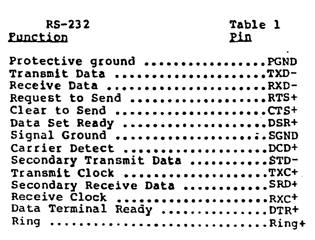
- The acronyms used in the table are identical to those conventionally used within the EIA standards and will not be further explained here. In Figures 2 and 3, the acronyms listed in Table 1 or 2 are employed to identify the lines on which the signals appear and will have a suffix "A" or "B" according to whether the line and signal is associated with channel A or channel B.
- Again, no detail will be given concerning the exact significance of these signals and how they may be employed to advantage in the overall computer operating system because they are not relevant to understanding and illustrating the present invention. Therefore, a detailed discussion of the RS-422 and RS-232 protocols as used in computer operating system 12 through S10
communications control circuit 14 have been omitted here for the sake of clarity and in order to more specifically focus upon the significant features of the described invention. - As is readily apparent in Figures 2 and 3, channel B of the operatively associated
S10 circuit 16 and register 18 communicates directly with interface circuitry indicated generally by reference number 19 comprising a plurality ofbuffer circuits buffers action S10 circuit 16 and register 18 in response to the input/output bus and various control inputs shown on the top, bottom and left side of Figures 2 and 3. In the case of the input/output bus signals, IOBO-IOB7, these lines are coupled directly to the input/output bus 12. The other S10 control signals, MR, Ml, RD, and so forth, are actually derived from specific, discrete, control signals and discrete logic circuitry also included withincircuit 14 to effectuate the options and performance designed into computer operating system 10. For the purposes of clarity, this discrete logic circuitry has been omitted from Figures 2 and 3 and it may be assumed that each signal line directed to the left side of Figures 2 and 3 is either directly coupled to input/output bus 12 or is indirectly coupled thereto through random logic circuitry included withcircuit 14, which circuitry generates the inputs to register 18 andS10 circuit 16 with an associated significance which is not material to understanding the present invention. - Referring now to channel A, its
interface circuitry 15 includes buffer circuitry for communicating according to the RS-422 protocol comprisingtransmitter buffer circuit 26 andreceiver buffer circuit 28. Similarly,interface circuitry 15 includes RS-232 buffer circuitry comprised oftransmitter buffer circuit 30 andreceiver buffer circuits - Channel A of the operatively associated
S10 circuit 16 and register 18 is switched between the RS-422 circuitry on one hand, and the RS-232 circuitry on the other hand by means of a switching assembly comprised of switches 36 and 38 in the case of the RS-422 buffer circuits; and switches 40 and 42 in the case of the RS-232 buffer circuitry. In the illustrated embodiment, switches 36-42 are comprised of dual-in-line packages proviaing connections through mating plugs and sockets and in which opposite pins are strapped together by a copper bus or conductor. Such jumper plugs are well-known to the art. Thus, as will be described below, the buffer circuitry of channel A can be configured by means of manually removing the jumper plugs from switches orsockets sockets 36 and 38. According to the present invention, removal of the plugs fromswitches switches 36 and 38 connects the RS-422 buffer circuitry. - Although the switching means or assembly has been described as a plurality of mechanical or manually manipulatable junction plugs and sockets in combination, it must be clearly kept in mind that many other modifications and alterations may be made by those having ordinary skill in the art without departing from the scope of the invention as defined in the claims below. For example, it is entirely within the scope of the present invention that the manually manipulatable/plug socket combination used in the preferred embodiment could be replaced by an equivalent switching circuit, enabled and disabled by discrete command signals originating in computer operating system 10.
- The circuitry and method of the present invention can be better understood by considering in detail the coupling of the RS-232 mode input and output lines of the
terminal device 11 through the switching assembly to channel A ofS10 circuit 16 and register 18. Considering only Figure 2, the RS-232 lines, other than protected and signal grounds, as listed in Table 1, are shown on the right hand edge of Figure 2 beginning at the top with the transmit clock signal for channel A, TXCA+ and ending-in the bottom with the ring indicator for channel A, RING A+. The jumper plugs are inserted inswitches switch 40 to the input ofreceiver 32, which is a conventional buffer circuit sold as type 1489. The outputs ofreceiver 32 are then coupled back throughswitch 40 at those points indicated by the arrows entirely included within therectangle representing switch 40. Each of the outputs fromreceiver 32 are then coupled to the corresponding inputs as labeled at the channel A input ports ofS10 circuit 16. - Similarly, the input lines DSRA+, SRDA+, RING A+, and DCDA+ are coupled as inputs through
switch 42 to the inputs ofreceiver 34, also a conventional buffer circuit sold as type 1489. The outputs ofreceiver 34 are then appropriately coupled to register 18 in the case of RING A+, DSRA+ and SRDA+ and to the appropriate channel A input ofS10 circuit 16 in the case of DCDA+. -
Transmitter 30, whose inputs are derived from the outputs DTRA-, RTSA-, TXDA+ of channel A ofS10 circuit 16 and from random logic ultimately coupled to the input/output bus, has its outputs coupled throughswitch 42 to the corresponding RS-232 output lines listed on the right side of Figure 2. - Thus, the entire RS-232 input/output pin configuration and protocol is appropriately coupled through
switches circuit 14.Switches terminal device 11 to the appropriate points within theS10 circuit 14, and they also isolate all receivers and transmitters from theterminal device 11, except those used in the selected protocol operating mode. When the RS-422 mode of operation is selected in place of the RS-232 mode of operation, the jumper plug of theswitch 42 is removed to isolate the outputs of thetransmitter 30 and inputs ofreceiver 34 from theterminal device 11.Switch 40 has its jumper plug removed to isolate the inputs of thereceiver 32 from theterminal device 11, as well. However, the outputs of thereceiver 32 are coupled to the same points within theS10 circuit 14 as certain outputs of thereceiver 28 used in the RS-422 mode. For this reason, the outputs of thereceiver 32 are advantageous couple to theS10 circuit 14 through theswitch 40 so that they are isolated from theterminal device 11 when the apparatus is in the RS-422 mode of operation. In this manner, the receivers and transmitters used in the RS-232 operating mode are isolated from the incompatible and potentially harmful voltage and current levels of signals present on the lines of theterminal device 11 when channel A of the apparatus is in the RS-422 mode of operation. - Figure 3 illustrates the
same interface circuitry 15 of Figure 2, but connected to operate in the RS-422 mode of operation. Figures 2 and 3 differ principally in the direction of arrows associated with the switches 36-42 signifying the direction of communication through theinterface circuitry 15 and acronyms which have been attributed to the input/output lines appearing on the right edge of Figure 3 as compared to those appearing on the right edge of Figure 2. Generally, a different significance is attributed to each of the input and output lines as a result of the switching executed by the switching assembly, principally switches 36 and 38. - Consider first the input lines at the upper right hand corner of Figure 3, namely RXCA-, RXCA+', TXCA+ and TXCA-. Each of these lines are coupled through
switch 36 to an input ofdifferential receiver 28. The signal on the line TXCA+ is matched with signal on the line TXCA- at the paired differential inputs ofreceiver 28.Receiver 28 is a conventional differential buffer circuit sold as type 26LS32. The upper two outputs ofreceiver 28 are coupled back throughswitch 36 and to the RXCA- and TXCA- channel A inputs ofS10 circuit 16. As in the case withreceiver 32, the inputs and outputs of the upper half ofreceiver 28 are completely isolated by removal of the jumper plug fromswitch 36. Again, the removal of the plug fromswitch 36 isolates the inputs and outputs of the upper half of thereceiver 28 from theterminal device 11 to protect that receiver from the incompatible and potentially harmful voltage and current levels of signals present on the lines of theterminal device 11 when channel A of the apparatus is placed in the RS-232 mode of operation in favor of the RS-232 mode of operation. - Similarly, the input lines CTSA+, CTSSA-, RXDA-and RXDA+ are coupled through the upper half of switch 38 to four matched inputs in the lower half of
receiver 28. The outputs carrying the clear-to-send signal and the read-data signal are coupled throughswitch 36, indicated by arrows totally contained within therectangle defining switch 36, to the received date, RXDA+, and clear-to-send and CTSA- inputs of the channel A port ofcircuit 16. Removal of the plugs fromswitches 36 and 38 protectively isolates the inputs and outputs of the lower half of thereceiver 28 as described hereinbefore with reference to the upper half of thereceiver 28. - Similarly, the inputs of
differential transmitter 26 on lines TXCA-, TXDA+, and RTSA- are derived from the appropriate channel A outputs ofcircuits 16 and are coupled through a conventional transmitter circuit sold astype 26LS31. The differential outputs oftransmitter 26 include the transmit clock signals, TXCA+ and TXCA-, which are coupled by correspondingly labeled output lines extending from transmitting 26 to the terminal 11. The other two pair of differential outputs or four outputs oftransmitter 26 are coupled through the lower half of switch 38 and appear at lines RTSA-, RTSA+, TXDA-, TXDA+ at the middle of the right hand edge of Figure 3, on which the remaining active portions of the RS-422 mode signals appear as summarized in Table 2. Removal of the plug from switch 38 protectively isolates the outputs of thetransmitter 26 from the potentially harmful current and voltage levels present on the lines of theterminal device 11 when channel A of the apparatus is in the RS-232 mode of operation. - Although the illustrated embodiment has been described in connection with certain specific types of circuitry implementing equally specific protocol modes, the innvention is much broader and could be applied to any application where an input/output circuit couples a local input/output bus through external peripherals operating under various synchronous and asynchronous bit and byte oriented protocols.
Claims (19)
the switching means selectively couples one of said plurality of receiver buffer circuits and one of said plurality of transmitter buffer circuits between said communication channel and said user terminal for forming the interface circuit configuration that communicates said communication channel and said user terminal according to the selected permissible protocol.
Applications Claiming Priority (2)
| Application Number | Priority Date | Filing Date | Title |
|---|---|---|---|
| US31151081A | 1981-10-15 | 1981-10-15 | |
| US311510 | 1994-09-23 |
Publications (2)
| Publication Number | Publication Date |
|---|---|
| EP0077657A2 true EP0077657A2 (en) | 1983-04-27 |
| EP0077657A3 EP0077657A3 (en) | 1983-07-06 |
Family
ID=23207225
Family Applications (1)
| Application Number | Title | Priority Date | Filing Date |
|---|---|---|---|
| EP82305495A Withdrawn EP0077657A3 (en) | 1981-10-15 | 1982-10-15 | Apparatus and methodology for configuration of an input/output digital circuit among different input/output protocols |
Country Status (2)
| Country | Link |
|---|---|
| EP (1) | EP0077657A3 (en) |
| JP (1) | JPS5876938A (en) |
Cited By (6)
| Publication number | Priority date | Publication date | Assignee | Title |
|---|---|---|---|---|
| EP0157113A2 (en) * | 1984-02-10 | 1985-10-09 | I.T.C. S.p.A. | An electronic interface device between a computer and external unit |
| FR2601474A1 (en) * | 1986-07-08 | 1988-01-15 | Pragma | Device for exchange of information between a fax machine and a microcomputer |
| EP0285390A2 (en) * | 1987-04-03 | 1988-10-05 | Neopost Limited | Franking machine |
| GB2241360A (en) * | 1990-02-05 | 1991-08-28 | Jupiter Technology Inc | Programmable data communication system |
| WO1995020194A1 (en) * | 1994-01-19 | 1995-07-27 | Siemens Aktiengesellschaft | Communication module |
| CN109297145A (en) * | 2018-09-29 | 2019-02-01 | 珠海格力电器股份有限公司 | Communicating circuit, communication device and air-conditioning |
Families Citing this family (2)
| Publication number | Priority date | Publication date | Assignee | Title |
|---|---|---|---|---|
| US4852127A (en) * | 1985-03-22 | 1989-07-25 | American Telephone And Telegraph Company, At&T Bell Laboratories | Universal protocol data receiver |
| JPH022776A (en) * | 1988-06-17 | 1990-01-08 | Nec Corp | Digital subscriber line transmission system |
Citations (2)
| Publication number | Priority date | Publication date | Assignee | Title |
|---|---|---|---|---|
| GB1116450A (en) * | 1964-12-03 | 1968-06-06 | Ass Elect Ind | Improvements relating to digital computer equipment |
| US4041473A (en) * | 1974-05-16 | 1977-08-09 | Honeywell Information Systems Italia | Computer input/output control apparatus |
-
1982
- 1982-10-14 JP JP57179165A patent/JPS5876938A/en active Pending
- 1982-10-15 EP EP82305495A patent/EP0077657A3/en not_active Withdrawn
Patent Citations (2)
| Publication number | Priority date | Publication date | Assignee | Title |
|---|---|---|---|---|
| GB1116450A (en) * | 1964-12-03 | 1968-06-06 | Ass Elect Ind | Improvements relating to digital computer equipment |
| US4041473A (en) * | 1974-05-16 | 1977-08-09 | Honeywell Information Systems Italia | Computer input/output control apparatus |
Non-Patent Citations (5)
| Title |
|---|
| COMPUTER DESIGN, vol. 20, no. 9, September 1981, pages 189-194, Winchester, Mass. (USA); M. PITCHER: "Serial input/output controller implements binary synchronous communication". * |
| COMPUTER DESIGN, vol. 21, no. 2, February 1982, pages 121-126, Winchester, Mass. (USA); R.A. GARROW: "Dual-bus design for a microcomputer". * |
| ELECTRONICS INTERNATIONAL, vol. 53, no. 8, April 1980, pages 135-140, New York (USA); G. SAWYER et al.: "Special-function modules ride on computer board". * |
| HEWLETT-PACKARD JOURNAL, vol. 33, no. 3, March 1982, pages 22-25, Amstelveen (NL); J.E. BEETEM: "The advanced terminal processor: a new terminal I/O controller for the HP 3000". * |
| IBM TECHNICAL DISCLOSURE BULLETIN, vol. 22, no. 6, November 1979, pages 2212-2213, New York (USA); G.E. LEIKAM et al.: "Programmable dual modem adapter for a communication interface". * |
Cited By (8)
| Publication number | Priority date | Publication date | Assignee | Title |
|---|---|---|---|---|
| EP0157113A2 (en) * | 1984-02-10 | 1985-10-09 | I.T.C. S.p.A. | An electronic interface device between a computer and external unit |
| EP0157113A3 (en) * | 1984-02-10 | 1986-07-02 | I.T.C. S.p.A. | An electronic interface device between a computer and external unit |
| FR2601474A1 (en) * | 1986-07-08 | 1988-01-15 | Pragma | Device for exchange of information between a fax machine and a microcomputer |
| EP0285390A2 (en) * | 1987-04-03 | 1988-10-05 | Neopost Limited | Franking machine |
| EP0285390A3 (en) * | 1987-04-03 | 1989-09-06 | Alcatel Business Systems Limited | Franking machine |
| GB2241360A (en) * | 1990-02-05 | 1991-08-28 | Jupiter Technology Inc | Programmable data communication system |
| WO1995020194A1 (en) * | 1994-01-19 | 1995-07-27 | Siemens Aktiengesellschaft | Communication module |
| CN109297145A (en) * | 2018-09-29 | 2019-02-01 | 珠海格力电器股份有限公司 | Communicating circuit, communication device and air-conditioning |
Also Published As
| Publication number | Publication date |
|---|---|
| JPS5876938A (en) | 1983-05-10 |
| EP0077657A3 (en) | 1983-07-06 |
Similar Documents
| Publication | Publication Date | Title |
|---|---|---|
| US5737364A (en) | Serial communications interface that supports multiple interface standards | |
| RU2577248C1 (en) | Adapter for electronic devices | |
| US6061754A (en) | Data bus having switch for selectively connecting and disconnecting devices to or from the bus | |
| US4700358A (en) | Synchronous/asynchronous modem | |
| EP3295318B1 (en) | Apparatus and methods for providing a reconfigurable bidirectional front-end interface | |
| EP1615135B1 (en) | Sharing single host controller with multiple functional devices | |
| US4579407A (en) | Interface cable | |
| EP0066605B1 (en) | Chip topography for integrated circuit communication controller | |
| JPH05236061A (en) | Interface sub-system applicable to plural interface standards | |
| EP1548607B1 (en) | Method of providing a microcontroller having an N-bit data bus width and a number of pins being equal or less than N | |
| GB1581836A (en) | Cpu-i/o bus interface for a data processing system | |
| EP0077657A2 (en) | Apparatus and methodology for configuration of an input/output digital circuit among different input/output protocols | |
| JP4478360B2 (en) | Data communication adapter | |
| US5799208A (en) | Apparatus for data communication between universal asynchronous receiver/transmitter (UART) modules and transceivers in a chip set by selectively connecting a common bus between multiplexer/demultiplexer units | |
| US4937464A (en) | Modular jack with loop testing switch | |
| GB1581839A (en) | I/o bus transceiver for a data processing system | |
| JPH01205222A (en) | Connector sharing device | |
| US10909060B2 (en) | Data transmission using flippable cable | |
| GB1581837A (en) | Peripheral device controller for a data processing system | |
| JPS6347106Y2 (en) | ||
| KR100202993B1 (en) | Conjunction apparatus between two connectors | |
| KR200337816Y1 (en) | ISDN Access Subscriber Matching Device in Electronic Switching System | |
| KR950002114Y1 (en) | Interface circuit | |
| AU586001B2 (en) | Virtual bus switching system | |
| US5949824A (en) | Two connector SIMM format interface circuit |
Legal Events
| Date | Code | Title | Description |
|---|---|---|---|
| PUAI | Public reference made under article 153(3) epc to a published international application that has entered the european phase |
Free format text: ORIGINAL CODE: 0009012 |
|
| AK | Designated contracting states |
Designated state(s): DE FR GB |
|
| PUAL | Search report despatched |
Free format text: ORIGINAL CODE: 0009013 |
|
| AK | Designated contracting states |
Designated state(s): DE FR GB |
|
| 17P | Request for examination filed |
Effective date: 19831017 |
|
| STAA | Information on the status of an ep patent application or granted ep patent |
Free format text: STATUS: THE APPLICATION IS DEEMED TO BE WITHDRAWN |
|
| 18D | Application deemed to be withdrawn |
Effective date: 19841204 |
|
| RIN1 | Information on inventor provided before grant (corrected) |
Inventor name: GARROW, ROBERT A. Inventor name: KIREMIDJIAN, FREDERICK Inventor name: LOWENTHAL, RICHARD W. |