EP3295318B1 - Apparatus and methods for providing a reconfigurable bidirectional front-end interface - Google Patents
Apparatus and methods for providing a reconfigurable bidirectional front-end interface Download PDFInfo
- Publication number
- EP3295318B1 EP3295318B1 EP16710661.6A EP16710661A EP3295318B1 EP 3295318 B1 EP3295318 B1 EP 3295318B1 EP 16710661 A EP16710661 A EP 16710661A EP 3295318 B1 EP3295318 B1 EP 3295318B1
- Authority
- EP
- European Patent Office
- Prior art keywords
- usb
- circuit
- mode
- signals
- transistor
- Prior art date
- Legal status (The legal status is an assumption and is not a legal conclusion. Google has not performed a legal analysis and makes no representation as to the accuracy of the status listed.)
- Active
Links
- 230000002457 bidirectional effect Effects 0.000 title claims description 69
- 238000000034 method Methods 0.000 title description 8
- 238000004891 communication Methods 0.000 claims description 6
- 229910044991 metal oxide Inorganic materials 0.000 claims description 4
- 150000004706 metal oxides Chemical class 0.000 claims description 4
- 239000004065 semiconductor Substances 0.000 claims description 4
- 230000005540 biological transmission Effects 0.000 description 13
- 230000008878 coupling Effects 0.000 description 9
- 238000010168 coupling process Methods 0.000 description 9
- 238000005859 coupling reaction Methods 0.000 description 9
- 239000003990 capacitor Substances 0.000 description 8
- 230000008901 benefit Effects 0.000 description 6
- 238000010586 diagram Methods 0.000 description 4
- 239000004020 conductor Substances 0.000 description 3
- 230000000295 complement effect Effects 0.000 description 1
- 238000001914 filtration Methods 0.000 description 1
- 238000004519 manufacturing process Methods 0.000 description 1
- 230000013011 mating Effects 0.000 description 1
Images


Classifications
-
- G—PHYSICS
- G06—COMPUTING; CALCULATING OR COUNTING
- G06F—ELECTRIC DIGITAL DATA PROCESSING
- G06F13/00—Interconnection of, or transfer of information or other signals between, memories, input/output devices or central processing units
- G06F13/38—Information transfer, e.g. on bus
- G06F13/42—Bus transfer protocol, e.g. handshake; Synchronisation
- G06F13/4282—Bus transfer protocol, e.g. handshake; Synchronisation on a serial bus, e.g. I2C bus, SPI bus
-
- G—PHYSICS
- G06—COMPUTING; CALCULATING OR COUNTING
- G06F—ELECTRIC DIGITAL DATA PROCESSING
- G06F13/00—Interconnection of, or transfer of information or other signals between, memories, input/output devices or central processing units
- G06F13/14—Handling requests for interconnection or transfer
- G06F13/36—Handling requests for interconnection or transfer for access to common bus or bus system
-
- G—PHYSICS
- G06—COMPUTING; CALCULATING OR COUNTING
- G06F—ELECTRIC DIGITAL DATA PROCESSING
- G06F13/00—Interconnection of, or transfer of information or other signals between, memories, input/output devices or central processing units
- G06F13/38—Information transfer, e.g. on bus
- G06F13/382—Information transfer, e.g. on bus using universal interface adapter
- G06F13/387—Information transfer, e.g. on bus using universal interface adapter for adaptation of different data processing systems to different peripheral devices, e.g. protocol converters for incompatible systems, open system
-
- G—PHYSICS
- G06—COMPUTING; CALCULATING OR COUNTING
- G06F—ELECTRIC DIGITAL DATA PROCESSING
- G06F13/00—Interconnection of, or transfer of information or other signals between, memories, input/output devices or central processing units
- G06F13/38—Information transfer, e.g. on bus
- G06F13/40—Bus structure
- G06F13/4004—Coupling between buses
- G06F13/4022—Coupling between buses using switching circuits, e.g. switching matrix, connection or expansion network
-
- G—PHYSICS
- G06—COMPUTING; CALCULATING OR COUNTING
- G06F—ELECTRIC DIGITAL DATA PROCESSING
- G06F13/00—Interconnection of, or transfer of information or other signals between, memories, input/output devices or central processing units
- G06F13/38—Information transfer, e.g. on bus
- G06F13/40—Bus structure
- G06F13/4063—Device-to-bus coupling
- G06F13/4068—Electrical coupling
- G06F13/4072—Drivers or receivers
-
- G—PHYSICS
- G06—COMPUTING; CALCULATING OR COUNTING
- G06F—ELECTRIC DIGITAL DATA PROCESSING
- G06F13/00—Interconnection of, or transfer of information or other signals between, memories, input/output devices or central processing units
- G06F13/38—Information transfer, e.g. on bus
- G06F13/40—Bus structure
- G06F13/4063—Device-to-bus coupling
- G06F13/4068—Electrical coupling
- G06F13/4086—Bus impedance matching, e.g. termination
Definitions
- This application relates to computing device connectors and, more specifically, to a reconfigurable bidirectional front-end interface suitable for transmitting and receiving signals.
- Computing devices may be equipped with one or more connectors that may provide connection, communication, and a power supply to a device. Such computing devices may use the connectors for various communications, including transferring and/or receiving signals. Examples of such computing devices may include, among others, personal computers, tablet computers, and smartphones.
- a connector may receive and transmit various types of signals complying with different standards, including, for example, Universal Serial Bus (USB) for data, Display Port (DP) for video, PCIe, and Audio Interface, among others.
- USB Universal Serial Bus
- DP Display Port
- Audio Interface among others.
- EP0942562 discloses a bi-directional, serial, differential bus driver circuit using PMOS and NMOS gates.
- Examples of devices that can benefit from one or more embodiments of the present application are input output devices, such as connectors.
- input output devices such as connectors.
- the following disclosure will continue with a USB 3.1 Type-C connector example to illustrate various embodiments of the present application.
- One example system embodiment includes a USB Controller and a Video Controller coupled to a reconfigurable USB SuperSpeed physical layer (USB-SS PHY) packaged as a system on chip (SoC), the outputs of which are coupled to a USB Type-C connector.
- USB-SS PHY includes a double lane USB-SS PHY (totaling four differential pair of lines) operable to be reconfigured dynamically as Display Port Alternative Mode lanes.
- the USB Controller utilizes two differential lines of the double lane USB-SS PHY for transmitting and two differential lines for receiving.
- Reconfiguring the physical layer for transmitting video signals in Display Port mode allows the Video Controller to utilize up to four differential lines for transmitting and four differential lines for receiving.
- four lines of the double lane USB-SS PHY are bidirectional and are operable to both transmit and receive signals, as compared to USB 3.1, where two unidirectional lines are dedicated for receiving signals and two unidirectional lines are dedicated for transmitting signals.
- USB2 mode may be operable during Display Port mode, allowing for the double lane USB-SS PHY to transmit/receive different types of signals.
- the double lane USB-SS PHY may be configured to support both USB 3.1 mode and Display Port mode substantially simultaneously, for example, by using one or more phase-locked loops (PLLs) to support different frequency of each mode.
- PLLs phase-locked loops
- transmit/receive terminals of a data line are coupled to USB 3.1 signals from a USB Controller and Display Port signals from a Video Controller. These transmit/receive terminals are also coupled to a shared terminating circuit for matching the characteristic impedance between the data lines when transmitting or receiving signals.
- Various embodiments described herein in more detail provide for using transistors to couple/decouple the Display Port signal paths and transistors to couple/decouple the shared terminating circuit to the transmit/receive terminals of the data line in order to allow reconfiguring of the terminals.
- FIG. 1A is a block diagram illustrating an example system 10, in accordance with various embodiments of the present disclosure.
- system 10 includes devices 20, 40, which are configured to communicate with each other.
- a cable 60 having plugs 62, 64, on both ends for mating with USB Type-C Connectors 22, 42 provides the communication path for Devices 20, 40.
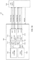
- Device 20 includes a SOC 24 including a USB SuperSpeed physical layer (PHY) 26, a USB Controller 28, a Video Controller 30, and one or more other modules 32, coupled together and configured for receiving and transmitting signals to and from the USB Type-C Connector 22.
- PHY USB SuperSpeed physical layer
- FIG. 1B is a block diagram illustrating an example system 100, which corresponds with any one of device 20, 40 of FIG. 1A , in accordance with various embodiments of the present disclosure.
- the system 100 allows for transmitting and receiving different types of signals.
- the different types of signals are USB 3.1 and Display Port signals.
- USB 3.1/DataPort Type-C connector that transmits/receives USB 3.1 and Display Port signals example, to illustrate various principles, it is understood that the disclosure is not limited to USB 3.1/DataPort Type-C connector or to USB 3.1 and Display Port signals.
- the System 100 allows for dynamic reconfiguring at the physical layer, when operating in USB 3.1 mode and Display Port mode.
- the system 100 includes a SOC 102 coupled to a USB Type-C Connector 104.
- the system 100 may be implemented on a single board that includes both the SOC 102 and the USB Type-C Connector 104.
- the SOC 102 includes a USB Controller 106, a Video Controller 108, and a reconfigurable first 110 and second 112 USB SuperSpeed lane physical layer (USB SS1 PHY and USB SS2 PHY).
- USB SS1 PHY and USB SS2 PHY USB SuperSpeed lane physical layer
- elements 110 and 112 may also be referred to herein as a double lane reconfigurable USB-SS PHY 110 and 112.
- a USB SuperSpeed Physical Coding Sublayer (USB SS PCS) 114 is coupled to and between the USB Controller 106 and the double lane reconfigurable USB-SS PHY 110 and 112 by connections 118 and 120.
- the USB SS PCS 114 includes digital control logic for receiving the USB Controller 106 signals, which may be transmitted via connection 118 in parallel as bits of data.
- the USB SS PCS 114 is operable to decode the signals from the USB Controller 106, and convert them into suitable analog signals for utilization by the analog circuits of the double lane reconfigurable USB-SS PHY 110 and 112.
- a Display Port power controls state (DP PCS) 116 is coupled to and between the Video Controller 108 and the double lane reconfigurable USB-SS PHY 110 and 112 by connections 122 and 120.
- the DP PCS 116 includes digital control logic for receiving the Video Controller 108 signals, which may be transmitted via connection 122 in parallel as bits of data.
- the DP PCS 116 is operable to decode the signals and convert them into suitable analog signals for utilization by the analog circuits of the double lane reconfigurable USB-SS PHY 110 and 112.
- connection 120 provides a multiplexing function, at the physical layer, on the analog signals received from the USB SS PCS 14 and DP PCS 116, thereby reducing device cost and improving performance since the multiplexing is performed on the lower rate parallel signals (as compared to higher speed multiplexing on serial signals).
- the SOC 102 may also include other modules, for example, one or more processing cores, a modem, other circuits, and logic. The scope of embodiments is not limited to SoCs circuits unless specifically claimed.
- the first and second reconfigurable USB-SS PHY 110, 112 are coupled to four differential data lines including: Line 1 TX1/RX3 P/N, Line 2 TX3/RX1 P/N, Line 3 TX2/RX4 P/N, and Line 4 TX4/RX2 P/N.
- the data Lines 1 to 4 are reconfigurable and bidirectional and can be utilized for both receiving and transmitting differential signals. Differential signals are used for differential encoding where the same electrical signal, of opposite polarity, is transmitted over the pair of data lines. The receiving circuit evaluates the difference between the two signals to determine the final value.
- the four pair of data lines for coupling the double lane reconfigurable USB-SS PHY 110 and 112 to the USB Type-C Connector 104 may be twisted pair, traces on a printed circuit board and/or chip, conductors in a coaxial cable, ribbon cable, or any other suitable cable, or any other suitable means based on design requirements.
- Different types of signals complying with different standards may be transmitted from the double lane reconfigurable USB-SS PHY 110 and 112 to the USB Type-C Connector 104 at the same time or at different times.
- transmitted signals may comply with, for example, USB 3.1, Display Port, High-Definition Multimedia Interface (HDMI), and other standards.
- other signals, including power/ground voltages may be provided over other lines of the USB Type-C Connector 104.
- a MODE signal may be transmitted from the USB-Type-C connector 104 back to the USB-SS PHY 110 and 112 and/or to a controller on the SoC 102 to indicate in which mode, corresponding to one or more standards, to operate.
- the following disclosure will continue with a USB 3.1 mode and a Display Port mode example to illustrate various embodiments of the present application. It is understood, however, that the application should not be limited to a particular type of mode, except as specifically claimed.
- the four differential pair lines of the double lane USB-SS 110 and 112 are set to operate in USB 3.1 mode.
- Line 1 operates as a transmission line (TX1 P/N)
- Line 2 operates as a reception line (RX1 P/N)
- Line 3 operates as a transmission line (TX2 P/N)
- Line 4 operate as a reception line (RX2 P/N).
- two lines of the double lane USB-SS PHY 110 and 112 may be operable to transmit video signals from the USB Controller 106 to the USB Type-C Connector 104 and two lines may be operable to receive signals.
- USB Type-C Connector 104 can receive a plug in either orientation (i.e., a plug can rotate 180 degrees), although all four lines may be active only two will be utilized in this example.
- plug orientation only one of the double lane USB-SS 110 and 112 is operable to transmit and receive signals, and the other is idle.
- the first reconfigurable USB-SS 112 may be idle and USB-SS 110 may be operable with Line 1 used for transmitting signals and Line 2 used for receiving signals.
- the first reconfigurable USB-SS 110 may be idle and USB-SS 112 may be operable with Line 3 used for transmitting data and Line 4 used for receiving signals.
- the double lane USB-SS 110 and 112 may be operable to be reconfigured to accommodate an improperly manufactured cable that has lines switched. For example, when the cable has Line 1 switched with Line 2, Line 1 operates as TX3/RX1 P/N and Line 2 operates as TX1/RX3 P/N.
- the four lines of the double lane USB-SS 110 and 112 are set to operate in Display Port mode.
- the lines when in Display Port mode the lines are set to transmit video signals such that Line 1 operates as a transmission line (TX1 P/N), Line 2 is reconfigured and operates as a transmission line (TX3 P/N), Line 3 operates as a transmission line (TX2 P/N), and Line 4 is reconfigured and operates as a transmission line (TX4 P/N).
- TX1 P/N Transmission line
- Line 2 is reconfigured and operates as a transmission line (TX3 P/N)
- Line 3 operates as a transmission line (TX2 P/N)
- Line 4 is reconfigured and operates as a transmission line (TX4 P/N).
- all of the lines of the double lane USB-SS PHY 110 and 112 may be active to transmit video signals from the Video Controller 108 to the USB Type-C Connector 104.
- the USB Type-C Connector 104 and plug orientation may be correctly aligned, allowing for transmitting up to four signals (one signal per line) from Video Controller 108.
- the four lines of the double lane USB-SS 110 and 112 may be active and each line transmitting one signal from the Video Controller 108.
- the lines when in Display Port mode, operate as reception lines allowing for the Video Controller 108 to receive signals from external devices connected to the USB Type-C Connector 104.
- Line 1 is reconfigured and operates as a reception line (RX3 P/N)
- Line 2 operates as a reception line (RX1 P/N)
- Line 3 reconfigured and operates as a reception line (RX4 P/N)
- Line 4 operates as a reception line (RX2 P/N).
- all of the lines of the double lane USB-SS PHY 110 and 112 may be active to receive video signals from a device coupled to the USB Type-C Connector 104 through a plug.
- the USB Type-C Connector 104 and plug orientation may be correctly aligned, allowing for receiving up to four signals (one signal per line) from a video controller of the plugged in device.
- the four lines of the double lane USB-SS 110 and 112 may be active and each line receiving one signal from an external device, which is received by the Video Controller 108.
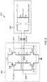
- FIG. 2 shows an exemplary implementation of a bidirectional lane front-end circuit 200 according to an embodiment of the present disclosure.
- the bidirectional lane front-end circuit 200 is useful for providing dynamic reconfiguration for different modes at the physical layer.
- the bidirectional lane front-end circuit 200 may be implemented as part of the first reconfigurable USB-SS PHY 110 and/or the second reconfigurable USB-SS PHY 112, within the SOC 102 of the embodiment of FIGS. 1A and 1B .
- the bidirectional lane front-end circuit 200 is referred to as bidirectional because the front terminals, i.e., TX_RXP and TX_RXN, can both transmit and receive signals.
- the bidirectional lane front-end circuit 200 includes a voltage mode transmitter (TX) circuit 202, a receiver (RX) circuit 204, and a shared terminating impedance circuit 206 included as part of the voltage mode TX circuit 202.
- the voltage mode TX circuit 202 has two parallel inverters.
- the voltage mode TX circuit 202 includes an input voltage source Vdd, a first input p-channel metal oxide semiconductor (PMOS) transistor 208, a second input PMOS transistor 210, and a first and second resistor R D1,2 .
- PMOS metal oxide semiconductor
- the source of the PMOS transistors 208 and 210 are coupled to Vdd.
- the gate input of the PMOS transistor 208 is coupled to the TXP_term
- the drain of the PMOS transistor 208 is coupled to a first resistor R 1
- the other side of the first resistor R 1 is coupled to the TX_RXP bidirectional terminal through data line 212.
- the gate input of the PMOS transistor 210 is coupled to the TXN_term
- the drain of the PMOS transistor 210 is coupled to a second resistor R 2
- the other side of the second resistor R 2 is coupled to the TX_RXN bidirectional terminal through data line 214.
- the TXP_term and the TXN_term that receive the P and N input signals are unidirectional terminals.
- Each of the first and second resistors R 1,2 may be implemented with one or more resistors (in series or parallel) and may be selected to accommodate different types of transmission and/or reception signals based on protocol utilized and desired impedance.
- the PMOS transistors 208 and 210 act as switches that couple the Display Port signals from the Video Controller 108 received through the P and N input signals to the TX_RXP and TX_RXN bidirectional terminals, and also isolate (or decouple) the transmitting voltage when Display Port mode is not active.
- the shared terminating impedance circuit 206 is part of the voltage mode TX circuit 202.
- the shared terminating impedance circuit 206 includes a third resistor R 3 coupled to the TX_RXP terminal through data line 212 and a fourth resistor R 4 coupled to the TX_RXN terminal through data line 214.
- An n-channel metal oxide semiconductor (NMOS) transistor 216 is coupled to the other terminal of the third resistor R 3 and a second NMOS transistor 218 is coupled to the other terminal of the fourth resistor R 4 .
- NMOS metal oxide semiconductor
- the NMOS transistors 216 and 218 act as switches allowing for biasing the voltage output when transmitting in Display Port mode and for impedance matching between the data lines 212 and 214 and the Type-C Connector 104 when receiving in USB 3.1 mode.
- the gate input to the NMOS transistor 216 is common with the gate input to the PMOS transistor 208 and receives a P input signal through the TXP_term
- the gate input to the NMOS transistor 218 is common with the gate input to the PMOS transistor 210 and receives the N input signal through the TXN_term.
- the P and N input signals are used to control the mode of operation of the circuit, and when in Display Port mode provide video signals by outputting the P and N signal to the bidirectional TX_RXP and TX_RXN terminals, as discussed below in connection with Table 1.
- Each of the third and fourth resistors R 3,4 may include one or more resistors (in series or parallel) and a plurality of impedance switches (not shown).
- each of the plurality of impedance switches controls whether one (or more) of the resistors is switched into a resistor network thereby setting the impedance of that terminating resistor.
- the impedance of the shared terminating impedance circuit 206 is referred to as "shared terminating impedance" because the impedance is utilized when transmitting and receiving signals and the data lines to which they are coupled terminate at the Type-C Connector.
- the third and fourth resistors R 3,4 are used to bias the output voltage and to provide a DC current path to ground.
- the third and fourth resistors R 3,4 are used to provide terminating impedance matching.
- the impedance of the third and fourth resistors R 3,4 may be selected to accommodate different types of transmission lines (e.g., twisted pair, traces on a printed circuit board and/or chip, conductors in a coaxial cable, ribbon cable, or any other suitable cable) that extend from the TX_RXP and TX_RXN terminals to the USB Type-C Connector 104.
- the impedance of the third and fourth resistors R 3,4 may be selected to accommodate different types of transmission and/or reception signals based on protocol utilized.
- each of the third and fourth resistors R 3,4 are single resistors having a value of about 50 ohms and the transmission line extending from the TX_RXP and TX_RXN terminals to the USB Type-C Connector 104 has an impedance of about 50 ohms.
- the RX circuit 204 includes a first capacitor C 1 coupled to the TX_RXP terminal and a second capacitor C 2 coupled to the TX_RXN terminal.
- the RX circuit 204 further includes fifth and sixth resistors R 5,6 coupled to the other terminals of the two capacitors C 1,2 , respectively, and a common-mode voltage VCM coupled between the fifth and sixth resistors R 5,6 .
- the split termination with the two capacitors C 1,2 is useful for providing filtering to eliminate common-mode noise that may be present between the complementary signals of the differential pair RXP_term and RXN_term.
- RXP_term and RXN_term are unidirectional terminals operable to receive signals.
- the fifth and sixth resistors R 5,6 may be implemented with one or more resistors (in series or parallel) and each of the two capacitors C 1,2 may be implemented with one or more capacitors (in series or parallel).
- the impedance of the fifth and sixth resistors R 5,6 may be selected to allow for a pullup and pulldown combination for terminating different types of transmission lines (e.g., twisted pair, traces on a printed circuit board and/or chip, conductors in a coaxial cable, ribbon cable, or any other suitable cable) that extend from the TX_RXP and TX_RXN terminals to the USB Type-C Connector 104.
- the values of the fifth and sixth resistors R 5,6 and the two capacitors C 1,2 may be selected to accommodate different types of transmission and/or reception signals based on protocol utilized.
- Each of the first and second reconfigurable USB-SS PHY 110 and 112 may include the bidirectional lane front-end circuit 200.
- a first bidirectional lane front-end circuit 200 is implemented as part of the first reconfigurable USB-SS PHY 110 where the shared terminating impedance circuit 206 provides matching characteristic impedances of the two data lines of Line 1 (TX1/RX3 P/N) of the first reconfigurable USB-SS PHY 110.
- a second bidirectional lane front-end circuit 200 is implemented as part of the first reconfigurable USB-SS PHY 110, where the shared terminating impedance circuit 206 provides matching characteristic impedances of the two data lines of Line 2 (TX3/RX1 P/N) of the first reconfigurable USB-SS PHY 110.
- a third bidirectional lane front-end circuit 200 is implemented as part of the second reconfigurable USB-SS PHY 112 and the shared terminating impedance circuit 206 provides matching characteristic impedances of the two data lines of Line 3 (TX2/RX4 P/N) of the second reconfigurable USB-SS PHY 112.
- a fourth bidirectional lane front-end circuit 200 is implemented as part of the second reconfigurable USB-SS PHY 112 and the shared terminating impedance circuit 206 provides matching characteristic impedances of the two data lines of Line 4 (TX4/RX2 P/N) of the second reconfigurable USB-SS PHY 112.
- the embodiments are not mutually exclusive and four bidirectional lane front-end circuits 200 may be included in the first and second reconfigurable USB-SS PHY 110 and 112.
- the Vdd voltage of the voltage mode TX circuit 202 is decoupled from the TX_RXP and TX_RXN bidirectional terminals by applying a logic one to the gate input of the PMOS transistor 208 and a logical one to the gate input of the PMOS transistor 210 via the P and N input signals at TXP_term and TXN_term, respectively.
- a logical one is applied to the gate input of the NMOS transistor 216 since the gate input of the NMOS transistor 216 is common with the gate input of the PMOS transistor 208, and a logical one is applied to the gate input of the NMOS transistor 218 since the gate input of the NMOS transistor 218 is common with the gate input of the PMOS transistor 210.
- the applied logical one at the gate input of the NMOS transistors 216 and 218 activates the shared terminating impedance circuit 206, providing a ground path.
- the shared terminating impedance circuit 206 is coupled to the TX_RXP and TX_RXN bidirectional terminals through the third and fourth resistors R 3,4 providing impedance matching when receiving signals.
- the input signals received through the TX_RXP and TX_RXN terminals are received at the differential pair RXP_term and RXN_term via the first and second capacitors C 1,2 and ultimately sent to the USB 3.1 controller 106 through the connection 120, USB SS PCS 114, and connection 118.
- the Vdd of the voltage mode TX circuit 202 is coupled to the TX_RXP terminal by applying a logic zero to the gate input of the PMOS transistor 208 via signal P at TXP_term. Since the gate input of the NMOS transistor 216 is common with the gate input of the PMOS transistor 208, a logical zero is also applied to the gate input of the NMOS transistor 216 thereby decoupling the TX_RXP terminal from ground.
- the Vdd of the voltage mode TX circuit 202 is coupled to the TX_RXN terminal by applying a logic zero to the gate input of the PMOS transistor 210 via signal N. Since the gate input of the NMOS transistor 218 is common with the gate input of the PMOS transistor 210, a logical zero is also applied to the gate input of the NMOS transistor 218 thereby decoupling the TX_RXP terminal from ground.
- a logic one is applied to the gate input of the PMOS transistor 208 via signal P.
- Applying the logic one via signal P decouples the Vdd from the TX_RXP terminal and since the gate input of the NMOS transistor 216 is common with the gate input of the PMOS transistor 208, a logical one is applied to the gate input of the NMOS transistor 216 thereby coupling the TX RXP bidirectional terminal to ground through resistor R 3 .
- Table 1 provided below summarizes the values of the TX_RXP and TX_RXN terminals based on the signal P/N at TXP_term and TXN_term. Table 1. MODE Signal P Signal N TX_RXP TX_RXN Receive 1 1 RXP RXN Transmit 1 0 TX (0) TX (1) Transmit 0 1 TX (1) TX (0)
- FIG. 1B by enabling dynamic reconfiguration of receiving lines into transmitting lines and transmitting lines into receiving lines within the PHY and sharing a termination circuit when transmitting and receiving, the embodiment of FIG. 1B allows for a smaller footprint/area on the SoC, allows for reusing four lines for transmitting and receiving, with the additional benefit of improving operational functionality (e.g., speed). Additional advantages of the embodiment of FIG. 1B include, not requiring a Crosspoint Switch, not requiring a multiplexer, not requiring a separate Video PHY, minimizing part cost, and simplifying manufacturing complexity. Further, the system disclosed herein is easily implemented into current devices. It is understood that different embodiments may have different advantages, and no particular advantage is necessarily required of any embodiment.
- FIG. 3 is an illustration of an example method 300, according to one embodiment, allows for dynamically reconfiguring data lines for transmitting and receiving different types of signals.
- the different types of signals are USB 3.1 and Display Port signals.
- method 300 provides for reconfiguring only the transmit lines (i.e., Lines 2 and 4) during Display Port mode, to illustrate various principles, it is understood that the disclosure is not limited by this example and the present disclosure additionally provides for reconfiguring the receiving lines (i.e., Lines 1 and 3) during Display Port mode.
- Method 300 may be performed by circuits, such as those shown in FIGS. 1A , 1B , and 2 .
- FIGS. 1A , 1B , and 2 show a system including a USB Type-C connector 104 that provides reception and/or transmission of different types of signals based on a mode of operation.
- Various embodiments include the actions of method 300 being performed by any of the circuits or combination of the circuits shown in FIGS. 1A , 1B , and 2 as appropriate.
- a MODE signal is provided.
- the MODE signal is provided by a first device plugged to the USB Type-C Connector 104.
- the MODE signal may be provided to one or more controllers, such as USB Controller 106 and/or Video Controller 108, or modules on a circuit board coupled to the USB Type-C Connector 104.
- the one or more controllers or modules may be within SoC 102 on the circuit board, such as that shown in FIG. 1B .
- a first control signal is generated in response to determining that the MODE signal is in a first mode.
- the first mode is USB 3.1 mode.
- the first control signal is generated by the USB Controller 106 and/or Video Controller 108, or other control modules on the SoC 102.
- the first control signal is applied to terminals of a bidirectional lane front-end circuit to configure the bidirectional lane front-end circuit to operate in the first mode.
- the USB Controller 106 and/or Video Controller 108, or other control modules on the SoC 102 may apply the first control signal to terminals TXP_term and TXN_term, of the bidirectional lane front-end circuit 200 illustrated in FIG. 2 .
- the bidirectional lane front-end circuit 200 may be included in a Universal Serial Bus SuperSpeed physical layer 110, 112 (USB SS PHY) of FIG. 1B .
- configuring the bidirectional lane front-end circuit 200 includes configuring a bidirectional terminal of Line 2 and/or Line 4 of the USB SS PHY 110, 112 to receive signals.
- Configuring the bidirectional terminal to receive signals may include coupling a first terminal TX_RXP and a second terminal TX_RXN, of the bidirectional terminal to a terminating impedance circuit 206, as shown in FIG 2 .
- Coupling the first terminal TX_RXP and the second TX_RXN terminal to the terminating circuit 206 may include switching on two transistors of an inverter circuit, as shown in FIG 2 .
- the bidirectional lane front-end circuit operates in the first mode.
- the first mode is USB 3.1 mode
- operating the bidirectional lane front-end circuit 200 in the first mode includes receiving a USB 3.1 signal over a bidirectional line, such as Lines 2 and 4, coupled to the bidirectional terminal of the USB SS PHY 110, 112.
- operating the bidirectional lane front-end circuit in the first mode may include transmitting a first USB 3.1 signal received from USB Controller 106 over the USB SS PHY 110 and 112 to the USB Type-C Connector 104 over a unidirectional line, such as Lines 1 and 3, and transmitting a second USB 3.1 signal received from the USB Type-C Connector 104 over the USB SS PHY 110 and 112 to the USB Controller 106 over a bidirectional line, such as Lines 2 and 4.
- the first and second signals may be handled simultaneously by the USB SS PHY.
- a second control signal is generated in response to determining that the MODE signal is in a second mode, different than the first mode.
- the second mode is Display Port mode.
- the second control signal is applied to terminals of the bidirectional lane front-end circuit to reconfigure the bidirectional lane front-end circuit to operate in the second mode.
- reconfiguring the bidirectional lane front-end circuit 200 to operate in the second mode includes reconfiguring the bidirectional terminal of the USB SS PHY to operate to transmit signals.
- configuring the bidirectional terminal of the USB SS PHY to operate to transmit signals includes coupling the first terminal TX_RXP of the bidirectional terminal to the terminating circuit 206 and coupling the second terminal TX_RXN of the bidirectional terminal to a voltage source Vdd.
- Coupling the first terminal TX_RXP to the terminating circuit 206 and coupling the second terminal TX_RXN to the voltage source Vdd includes switching on a first and a second transistor of an inverter circuit, such as that shown in FIG. 2 .
- the bidirectional lane front-end circuit operates in the second mode.
- operating in the second mode includes transmitting to the USB Type-C Connector 104 a first signal over a unidirectional line, such as Lines 1 and 3, coupled to the USB SS PHY 110, 112, and transmitting to the USB Type-C Connector 104 a second signal over a reconfigured bidirectional line, such as Lines 2 and 4, coupled to the bidirectional terminal of the USB SS PHY 110, 112, or over the remaining unidirectional terminal.
- the first and second signals may be transmitted simultaneously over the selected lines. Consequently, the example allows for transmitting of four different signals over Lines 1-4 simultaneously.
- Operating the bidirectional lane front-end circuit 200 in the second mode includes transmitting Display Port signals received from Video Controller 108.
- FIG. 3 provides an illustration where the first mode is USB 3.1 mode and the second mode is Display Port mode, these two modes may be swapped such that the Display Port mode is first and the USB 3.1 port mode is second. Also, it is understood that the above disclosure is not limited to USB 3.1 and Display Port modes and any different modes corresponding with two different protocols are contemplated and within the scope of this disclosure. Also, as noted above, although method 300 of FIG. 3 provides for reconfiguring two transmit lines during Display Port mode, it is understood that the present disclosure additionally provides for reconfiguring two receiving lines during Display Port mode, such that in Display Port mode all four lines can be configured to both transmit and receive video signals.
Description
- This application relates to computing device connectors and, more specifically, to a reconfigurable bidirectional front-end interface suitable for transmitting and receiving signals.
- Computing devices may be equipped with one or more connectors that may provide connection, communication, and a power supply to a device. Such computing devices may use the connectors for various communications, including transferring and/or receiving signals. Examples of such computing devices may include, among others, personal computers, tablet computers, and smartphones.
- A connector may receive and transmit various types of signals complying with different standards, including, for example, Universal Serial Bus (USB) for data, Display Port (DP) for video, PCIe, and Audio Interface, among others.
EP0942562 discloses a bi-directional, serial, differential bus driver circuit using PMOS and NMOS gates. - The accompanying drawings, which form a part of the specification, illustrate exemplary embodiments and together with the description, further serve to explain the principles of these exemplary embodiments. In the drawings, like reference numbers may indicate identical or functionally similar elements. The drawing in which an element first appears is generally indicated by the left-most digit in the corresponding reference number.
-
FIG. 1A is a block diagram illustrating an exemplary system, according to various embodiments. -
FIG. 1B is a block diagram illustrating an exemplary system, according to various embodiments. -
FIG. 2 is an exemplary bidirectional lane front-end circuit that may be used in the system ofFIGS. 1A and1B , according to various embodiments. -
FIG. 3 is a simplified flowchart illustrating a method for providing different modes of operation at the physical layer of a connector, according to various embodiments. - The scope of protection is defined by the appended claims.
- Examples of devices that can benefit from one or more embodiments of the present application are input output devices, such as connectors. The following disclosure will continue with a USB 3.1 Type-C connector example to illustrate various embodiments of the present application.
- Disclosed herein are embodiments of an apparatus and methods for a reconfigurable bidirectional front-end interface suitable for transmitting and receiving signals. One example system embodiment includes a USB Controller and a Video Controller coupled to a reconfigurable USB SuperSpeed physical layer (USB-SS PHY) packaged as a system on chip (SoC), the outputs of which are coupled to a USB Type-C connector. In one embodiment, the USB-SS PHY includes a double lane USB-SS PHY (totaling four differential pair of lines) operable to be reconfigured dynamically as Display Port Alternative Mode lanes. When configured for USB 3.1 signals, the USB Controller utilizes two differential lines of the double lane USB-SS PHY for transmitting and two differential lines for receiving. Reconfiguring the physical layer for transmitting video signals in Display Port mode, allows the Video Controller to utilize up to four differential lines for transmitting and four differential lines for receiving. As such, and of note, is that four lines of the double lane USB-SS PHY are bidirectional and are operable to both transmit and receive signals, as compared to USB 3.1, where two unidirectional lines are dedicated for receiving signals and two unidirectional lines are dedicated for transmitting signals.
- It is noted that other modes may be operable at the same time. For example, USB2 mode may be operable during Display Port mode, allowing for the double lane USB-SS PHY to transmit/receive different types of signals. Also, it is noted that the double lane USB-SS PHY may be configured to support both USB 3.1 mode and Display Port mode substantially simultaneously, for example, by using one or more phase-locked loops (PLLs) to support different frequency of each mode. As such, the scope of embodiments is not limited to any particular number of bidirectional lines and/or modes and any appropriate number of bidirectional lines and/or modes may be operable at the same or different times, in various embodiments.
- In one embodiment, to achieve the dynamic reconfiguring of the double lane USB-SS PHY, transmit/receive terminals of a data line are coupled to USB 3.1 signals from a USB Controller and Display Port signals from a Video Controller. These transmit/receive terminals are also coupled to a shared terminating circuit for matching the characteristic impedance between the data lines when transmitting or receiving signals. Various embodiments described herein in more detail provide for using transistors to couple/decouple the Display Port signal paths and transistors to couple/decouple the shared terminating circuit to the transmit/receive terminals of the data line in order to allow reconfiguring of the terminals.
-
FIG. 1A is a block diagram illustrating anexample system 10, in accordance with various embodiments of the present disclosure. InFIG. 1A ,system 10 includesdevices cable 60, havingplugs C Connectors Devices Device 20 includes aSOC 24 including a USB SuperSpeed physical layer (PHY) 26, aUSB Controller 28, aVideo Controller 30, and one or moreother modules 32, coupled together and configured for receiving and transmitting signals to and from the USB Type-C Connector 22.Device 40 includes a SOC 44 including aPHY 46, aUSB Controller 48, aVideo Controller 50, and one or moreother modules 52, coupled together and configured for receiving and transmitting signals to and from the USB Type-C connector 42.Devices FIG. 1B is a block diagram illustrating anexample system 100, which corresponds with any one ofdevice FIG. 1A , in accordance with various embodiments of the present disclosure. In the present embodiment, thesystem 100 allows for transmitting and receiving different types of signals. In the present embodiment, the different types of signals are USB 3.1 and Display Port signals. Although the system ofFIG. 1B provides a USB 3.1/DataPort Type-C connector that transmits/receives USB 3.1 and Display Port signals example, to illustrate various principles, it is understood that the disclosure is not limited to USB 3.1/DataPort Type-C connector or to USB 3.1 and Display Port signals. -
System 100 allows for dynamic reconfiguring at the physical layer, when operating in USB 3.1 mode and Display Port mode. Thesystem 100 includes aSOC 102 coupled to a USB Type-C Connector 104. Thesystem 100 may be implemented on a single board that includes both the SOC 102 and the USB Type-C Connector 104. The SOC 102 includes aUSB Controller 106, aVideo Controller 108, and a reconfigurable first 110 and second 112 USB SuperSpeed lane physical layer (USB SS1 PHY and USB SS2 PHY). Collectively,elements SOC 102 into redundant signals before reaching the USB Type-C Connector 104. - A USB SuperSpeed Physical Coding Sublayer (USB SS PCS) 114 is coupled to and between the
USB Controller 106 and the double lane reconfigurable USB-SS PHY 110 and 112 byconnections USB Controller 106 signals, which may be transmitted viaconnection 118 in parallel as bits of data. The USB SS PCS 114 is operable to decode the signals from theUSB Controller 106, and convert them into suitable analog signals for utilization by the analog circuits of the double lane reconfigurable USB-SS PHY 110 and 112. - Similarly, a Display Port power controls state (DP PCS) 116 is coupled to and between the
Video Controller 108 and the double lane reconfigurable USB-SS PHY 110 and 112 byconnections Video Controller 108 signals, which may be transmitted viaconnection 122 in parallel as bits of data. The DP PCS 116 is operable to decode the signals and convert them into suitable analog signals for utilization by the analog circuits of the double lane reconfigurable USB-SS PHY 110 and 112. In the present embodiment,connection 120 provides a multiplexing function, at the physical layer, on the analog signals received from the USB SS PCS 14 and DP PCS 116, thereby reducing device cost and improving performance since the multiplexing is performed on the lower rate parallel signals (as compared to higher speed multiplexing on serial signals). The SOC 102 may also include other modules, for example, one or more processing cores, a modem, other circuits, and logic. The scope of embodiments is not limited to SoCs circuits unless specifically claimed. - In one embodiment, the first and second reconfigurable USB-
SS PHY Line 1 TX1/RX3 P/N,Line 2 TX3/RX1 P/N,Line 3 TX2/RX4 P/N, andLine 4 TX4/RX2 P/N. Notably, the data Lines 1 to 4 are reconfigurable and bidirectional and can be utilized for both receiving and transmitting differential signals. Differential signals are used for differential encoding where the same electrical signal, of opposite polarity, is transmitted over the pair of data lines. The receiving circuit evaluates the difference between the two signals to determine the final value. - The four pair of data lines for coupling the double lane reconfigurable USB-
SS PHY C Connector 104 may be twisted pair, traces on a printed circuit board and/or chip, conductors in a coaxial cable, ribbon cable, or any other suitable cable, or any other suitable means based on design requirements. - Different types of signals complying with different standards may be transmitted from the double lane reconfigurable USB-
SS PHY C Connector 104 at the same time or at different times. For example, transmitted signals may comply with, for example, USB 3.1, Display Port, High-Definition Multimedia Interface (HDMI), and other standards. Also, other signals, including power/ground voltages may be provided over other lines of the USB Type-C Connector 104. In one embodiment, depending on the type of device connected to the USB Type-C Connector 104, a MODE signal may be transmitted from the USB-Type-C connector 104 back to the USB-SS PHY SoC 102 to indicate in which mode, corresponding to one or more standards, to operate. The following disclosure will continue with a USB 3.1 mode and a Display Port mode example to illustrate various embodiments of the present application. It is understood, however, that the application should not be limited to a particular type of mode, except as specifically claimed. - When the MODE signal indicates USB 3.1 mode, the four differential pair lines of the double lane USB-
SS Line 1 operates as a transmission line (TX1 P/N),Line 2 operates as a reception line (RX1 P/N),Line 3 operates as a transmission line (TX2 P/N), andLine 4 operate as a reception line (RX2 P/N). As such, in USB 3.1 mode, two lines of the double lane USB-SS PHY USB Controller 106 to the USB Type-C Connector 104 and two lines may be operable to receive signals. However, since the USB Type-C Connector 104 can receive a plug in either orientation (i.e., a plug can rotate 180 degrees), although all four lines may be active only two will be utilized in this example. As such, based on plug orientation, only one of the double lane USB-SS SS 112 may be idle and USB-SS 110 may be operable withLine 1 used for transmitting signals andLine 2 used for receiving signals. Alternatively, based on plug orientation the first reconfigurable USB-SS 110 may be idle and USB-SS 112 may be operable withLine 3 used for transmitting data andLine 4 used for receiving signals. The double lane USB-SS Line 1 switched withLine 2,Line 1 operates as TX3/RX1 P/N andLine 2 operates as TX1/RX3 P/N. - When the MODE signal indicates Display Port mode, the four lines of the double lane USB-
SS Line 1 operates as a transmission line (TX1 P/N),Line 2 is reconfigured and operates as a transmission line (TX3 P/N),Line 3 operates as a transmission line (TX2 P/N), andLine 4 is reconfigured and operates as a transmission line (TX4 P/N). As such, in Display Port mode, all of the lines of the double lane USB-SS PHY Video Controller 108 to the USB Type-C Connector 104. The USB Type-C Connector 104 and plug orientation may be correctly aligned, allowing for transmitting up to four signals (one signal per line) fromVideo Controller 108. As such, in one embodiment while in Display Port mode, the four lines of the double lane USB-SS Video Controller 108. - In alternative embodiments, when in Display Port mode, the lines operate as reception lines allowing for the
Video Controller 108 to receive signals from external devices connected to the USB Type-C Connector 104. In such embodiments,Line 1 is reconfigured and operates as a reception line (RX3 P/N),Line 2 operates as a reception line (RX1 P/N),Line 3 reconfigured and operates as a reception line (RX4 P/N), andLine 4 operates as a reception line (RX2 P/N). As such, in Display Port mode, all of the lines of the double lane USB-SS PHY C Connector 104 through a plug. The USB Type-C Connector 104 and plug orientation may be correctly aligned, allowing for receiving up to four signals (one signal per line) from a video controller of the plugged in device. As such, in one embodiment while in Display Port mode, the four lines of the double lane USB-SS Video Controller 108. -
FIG. 2 shows an exemplary implementation of a bidirectional lane front-end circuit 200 according to an embodiment of the present disclosure. The bidirectional lane front-end circuit 200 is useful for providing dynamic reconfiguration for different modes at the physical layer. The bidirectional lane front-end circuit 200 may be implemented as part of the first reconfigurable USB-SS PHY 110 and/or the second reconfigurable USB-SS PHY 112, within theSOC 102 of the embodiment ofFIGS. 1A and1B . The bidirectional lane front-end circuit 200 is referred to as bidirectional because the front terminals, i.e., TX_RXP and TX_RXN, can both transmit and receive signals. - The bidirectional lane front-
end circuit 200 includes a voltage mode transmitter (TX)circuit 202, a receiver (RX)circuit 204, and a shared terminatingimpedance circuit 206 included as part of the voltagemode TX circuit 202. In the illustrated embodiment, the voltagemode TX circuit 202 has two parallel inverters. The voltagemode TX circuit 202 includes an input voltage source Vdd, a first input p-channel metal oxide semiconductor (PMOS)transistor 208, a secondinput PMOS transistor 210, and a first and second resistor R D1,2. - The source of the
PMOS transistors PMOS transistor 208 is coupled to the TXP_term, the drain of thePMOS transistor 208 is coupled to a first resistor R 1 , and the other side of the first resistor R 1 is coupled to the TX_RXP bidirectional terminal throughdata line 212. Similarly, the gate input of thePMOS transistor 210 is coupled to the TXN_term, the drain of thePMOS transistor 210 is coupled to a second resistor R 2 , and the other side of the second resistor R 2 is coupled to the TX_RXN bidirectional terminal throughdata line 214. The TXP_term and the TXN_term that receive the P and N input signals are unidirectional terminals. - Each of the first and second resistors R 1,2 may be implemented with one or more resistors (in series or parallel) and may be selected to accommodate different types of transmission and/or reception signals based on protocol utilized and desired impedance. The
PMOS transistors Video Controller 108 received through the P and N input signals to the TX_RXP and TX_RXN bidirectional terminals, and also isolate (or decouple) the transmitting voltage when Display Port mode is not active. - As noted above, the shared terminating
impedance circuit 206 is part of the voltagemode TX circuit 202. The shared terminatingimpedance circuit 206 includes a third resistor R 3 coupled to the TX_RXP terminal throughdata line 212 and a fourth resistor R 4 coupled to the TX_RXN terminal throughdata line 214. An n-channel metal oxide semiconductor (NMOS)transistor 216 is coupled to the other terminal of the third resistor R 3 and asecond NMOS transistor 218 is coupled to the other terminal of the fourth resistor R 4 . TheNMOS transistors data lines C Connector 104 when receiving in USB 3.1 mode. The gate input to theNMOS transistor 216 is common with the gate input to thePMOS transistor 208 and receives a P input signal through the TXP_term, and the gate input to theNMOS transistor 218 is common with the gate input to thePMOS transistor 210 and receives the N input signal through the TXN_term. The P and N input signals are used to control the mode of operation of the circuit, and when in Display Port mode provide video signals by outputting the P and N signal to the bidirectional TX_RXP and TX_RXN terminals, as discussed below in connection with Table 1. - Each of the third and fourth resistors R 3,4 may include one or more resistors (in series or parallel) and a plurality of impedance switches (not shown). In such embodiments, each of the plurality of impedance switches controls whether one (or more) of the resistors is switched into a resistor network thereby setting the impedance of that terminating resistor. The impedance of the shared terminating
impedance circuit 206 is referred to as "shared terminating impedance" because the impedance is utilized when transmitting and receiving signals and the data lines to which they are coupled terminate at the Type-C Connector. - When transmitting signals in Display Port mode, the third and fourth resistors R 3,4 are used to bias the output voltage and to provide a DC current path to ground. When receiving signals in USB 3.1 mode, the third and fourth resistors R 3,4 are used to provide terminating impedance matching. The impedance of the third and fourth resistors R 3,4 may be selected to accommodate different types of transmission lines (e.g., twisted pair, traces on a printed circuit board and/or chip, conductors in a coaxial cable, ribbon cable, or any other suitable cable) that extend from the TX_RXP and TX_RXN terminals to the USB Type-
C Connector 104. Also, the impedance of the third and fourth resistors R 3,4 may be selected to accommodate different types of transmission and/or reception signals based on protocol utilized. In the present embodiment, each of the third and fourth resistors R 3,4 are single resistors having a value of about 50 ohms and the transmission line extending from the TX_RXP and TX_RXN terminals to the USB Type-C Connector 104 has an impedance of about 50 ohms. - The
RX circuit 204 includes a first capacitor C 1 coupled to the TX_RXP terminal and a second capacitor C 2 coupled to the TX_RXN terminal. TheRX circuit 204 further includes fifth and sixth resistors R 5,6 coupled to the other terminals of the two capacitors C 1,2 , respectively, and a common-mode voltage VCM coupled between the fifth and sixth resistors R 5,6 . The split termination with the two capacitors C 1,2 , is useful for providing filtering to eliminate common-mode noise that may be present between the complementary signals of the differential pair RXP_term and RXN_term. RXP_term and RXN_term are unidirectional terminals operable to receive signals. - The fifth and sixth resistors R 5,6 may be implemented with one or more resistors (in series or parallel) and each of the two capacitors C 1,2 may be implemented with one or more capacitors (in series or parallel). The impedance of the fifth and sixth resistors R 5,6 may be selected to allow for a pullup and pulldown combination for terminating different types of transmission lines (e.g., twisted pair, traces on a printed circuit board and/or chip, conductors in a coaxial cable, ribbon cable, or any other suitable cable) that extend from the TX_RXP and TX_RXN terminals to the USB Type-
C Connector 104. Also, the values of the fifth and sixth resistors R 5,6 and the two capacitors C 1,2 may be selected to accommodate different types of transmission and/or reception signals based on protocol utilized. - Each of the first and second reconfigurable USB-
SS PHY 110 and 112 (FIG. 1B ) may include the bidirectional lane front-end circuit 200. In one embodiment, a first bidirectional lane front-end circuit 200 is implemented as part of the first reconfigurable USB-SS PHY 110 where the shared terminatingimpedance circuit 206 provides matching characteristic impedances of the two data lines of Line 1 (TX1/RX3 P/N) of the first reconfigurable USB-SS PHY 110. Further, a second bidirectional lane front-end circuit 200 is implemented as part of the first reconfigurable USB-SS PHY 110, where the shared terminatingimpedance circuit 206 provides matching characteristic impedances of the two data lines of Line 2 (TX3/RX1 P/N) of the first reconfigurable USB-SS PHY 110. - In another embodiment, a third bidirectional lane front-
end circuit 200 is implemented as part of the second reconfigurable USB-SS PHY 112 and the shared terminatingimpedance circuit 206 provides matching characteristic impedances of the two data lines of Line 3 (TX2/RX4 P/N) of the second reconfigurable USB-SS PHY 112. Further, a fourth bidirectional lane front-end circuit 200 is implemented as part of the second reconfigurable USB-SS PHY 112 and the shared terminatingimpedance circuit 206 provides matching characteristic impedances of the two data lines of Line 4 (TX4/RX2 P/N) of the second reconfigurable USB-SS PHY 112. As already noted, the embodiments are not mutually exclusive and four bidirectional lane front-end circuits 200 may be included in the first and second reconfigurable USB-SS PHY - During operation, to receive signals, the Vdd voltage of the voltage
mode TX circuit 202 is decoupled from the TX_RXP and TX_RXN bidirectional terminals by applying a logic one to the gate input of thePMOS transistor 208 and a logical one to the gate input of thePMOS transistor 210 via the P and N input signals at TXP_term and TXN_term, respectively. Also, a logical one is applied to the gate input of theNMOS transistor 216 since the gate input of theNMOS transistor 216 is common with the gate input of thePMOS transistor 208, and a logical one is applied to the gate input of theNMOS transistor 218 since the gate input of theNMOS transistor 218 is common with the gate input of thePMOS transistor 210. The applied logical one at the gate input of theNMOS transistors impedance circuit 206, providing a ground path. As a result, the shared terminatingimpedance circuit 206 is coupled to the TX_RXP and TX_RXN bidirectional terminals through the third and fourth resistors R3,4 providing impedance matching when receiving signals. The input signals received through the TX_RXP and TX_RXN terminals are received at the differential pair RXP_term and RXN_term via the first and second capacitors C 1,2 and ultimately sent to the USB 3.1controller 106 through theconnection 120,USB SS PCS 114, andconnection 118. - To transmit signals, the Vdd of the voltage
mode TX circuit 202 is coupled to the TX_RXP terminal by applying a logic zero to the gate input of thePMOS transistor 208 via signal P at TXP_term. Since the gate input of theNMOS transistor 216 is common with the gate input of thePMOS transistor 208, a logical zero is also applied to the gate input of theNMOS transistor 216 thereby decoupling the TX_RXP terminal from ground. - Because the P and N signals are differential, substantially at the same time as applying a logic zero via signal P, a logic one is applied to the gate input of the
PMOS transistor 210 via signal N at TXN_term. Applying the logic one via signal N decouples the Vdd voltage from the TX_RXN terminal and since the gate input of theNMOS transistor 218 is common with the gate input of thePMOS transistor 210, a logical one is applied to the gate input of theNMOS transistor 218 thereby coupling the TX_RXN terminal to ground through resistor R 4 . - The Vdd of the voltage
mode TX circuit 202 is coupled to the TX_RXN terminal by applying a logic zero to the gate input of thePMOS transistor 210 via signal N. Since the gate input of theNMOS transistor 218 is common with the gate input of thePMOS transistor 210, a logical zero is also applied to the gate input of theNMOS transistor 218 thereby decoupling the TX_RXP terminal from ground. - Because the P and N are a differential pair, substantially at the same time as applying a logic zero via signal N, a logic one is applied to the gate input of the
PMOS transistor 208 via signal P. Applying the logic one via signal P decouples the Vdd from the TX_RXP terminal and since the gate input of theNMOS transistor 216 is common with the gate input of thePMOS transistor 208, a logical one is applied to the gate input of theNMOS transistor 216 thereby coupling the TX RXP bidirectional terminal to ground through resistor R 3 . - Table 1 provided below summarizes the values of the TX_RXP and TX_RXN terminals based on the signal P/N at TXP_term and TXN_term.
Table 1. MODE Signal P Signal N TX_RXP TX_RXN Receive 1 1 RXP RXN Transmit 1 0 TX (0) TX (1) Transmit 0 1 TX (1) TX (0) - Various embodiments may include advantages and disadvantages. In more detail, with reference to
system 100 ofFIG. 1B , by enabling dynamic reconfiguration of receiving lines into transmitting lines and transmitting lines into receiving lines within the PHY and sharing a termination circuit when transmitting and receiving, the embodiment ofFIG. 1B allows for a smaller footprint/area on the SoC, allows for reusing four lines for transmitting and receiving, with the additional benefit of improving operational functionality (e.g., speed). Additional advantages of the embodiment ofFIG. 1B include, not requiring a Crosspoint Switch, not requiring a multiplexer, not requiring a separate Video PHY, minimizing part cost, and simplifying manufacturing complexity. Further, the system disclosed herein is easily implemented into current devices. It is understood that different embodiments may have different advantages, and no particular advantage is necessarily required of any embodiment. -
FIG. 3 is an illustration of anexample method 300, according to one embodiment, allows for dynamically reconfiguring data lines for transmitting and receiving different types of signals. In the present embodiment, the different types of signals are USB 3.1 and Display Port signals. Although in thepresent embodiment method 300 provides for reconfiguring only the transmit lines (i.e.,Lines 2 and 4) during Display Port mode, to illustrate various principles, it is understood that the disclosure is not limited by this example and the present disclosure additionally provides for reconfiguring the receiving lines (i.e.,Lines 1 and 3) during Display Port mode. -
Method 300 may be performed by circuits, such as those shown inFIGS. 1A ,1B , and2 . Specifically,FIGS. 1A ,1B , and2 show a system including a USB Type-C connector 104 that provides reception and/or transmission of different types of signals based on a mode of operation. Various embodiments include the actions ofmethod 300 being performed by any of the circuits or combination of the circuits shown inFIGS. 1A ,1B , and2 as appropriate. - At
action 302, a MODE signal is provided. For instance, in the example ofFIG.1B , the MODE signal is provided by a first device plugged to the USB Type-C Connector 104. The MODE signal may be provided to one or more controllers, such asUSB Controller 106 and/orVideo Controller 108, or modules on a circuit board coupled to the USB Type-C Connector 104. The one or more controllers or modules may be withinSoC 102 on the circuit board, such as that shown inFIG. 1B . - At
action 304, a first control signal is generated in response to determining that the MODE signal is in a first mode. In the present embodiment, the first mode is USB 3.1 mode. Returning to the example ofFIG. 1B , the first control signal is generated by theUSB Controller 106 and/orVideo Controller 108, or other control modules on theSoC 102. - At
action 306, the first control signal is applied to terminals of a bidirectional lane front-end circuit to configure the bidirectional lane front-end circuit to operate in the first mode. For example, in the embodiment ofFIG. 1B , theUSB Controller 106 and/orVideo Controller 108, or other control modules on theSoC 102 may apply the first control signal to terminals TXP_term and TXN_term, of the bidirectional lane front-end circuit 200 illustrated inFIG. 2 . As noted above in connection with the embodiment ofFIG. 2 , the bidirectional lane front-end circuit 200 may be included in a Universal Serial Bus SuperSpeedphysical layer 110, 112 (USB SS PHY) ofFIG. 1B . - Referring back to
FIG. 2 , since in the present embodiment the first mode is USB 3.1 mode, configuring the bidirectional lane front-end circuit 200 includes configuring a bidirectional terminal ofLine 2 and/orLine 4 of theUSB SS PHY impedance circuit 206, as shown inFIG 2 . Coupling the first terminal TX_RXP and the second TX_RXN terminal to the terminatingcircuit 206 may include switching on two transistors of an inverter circuit, as shown inFIG 2 . - At
action 308, the bidirectional lane front-end circuit operates in the first mode. In the example ofFIG. 1B , since in the present embodiment the first mode is USB 3.1 mode, operating the bidirectional lane front-end circuit 200 in the first mode includes receiving a USB 3.1 signal over a bidirectional line, such asLines USB SS PHY USB Controller 106 over theUSB SS PHY C Connector 104 over a unidirectional line, such asLines C Connector 104 over theUSB SS PHY USB Controller 106 over a bidirectional line, such asLines - At
action 310, a second control signal is generated in response to determining that the MODE signal is in a second mode, different than the first mode. For instance, in the example ofFIG.1 ,USB Controller 106 and/orVideo Controller 108, or other modules, generate the second control signal. In the present embodiment, the second mode is Display Port mode. - At
action 312, the second control signal is applied to terminals of the bidirectional lane front-end circuit to reconfigure the bidirectional lane front-end circuit to operate in the second mode. Referring back to the example ofFIG. 2 , since the second mode is Display Port mode, reconfiguring the bidirectional lane front-end circuit 200 to operate in the second mode includes reconfiguring the bidirectional terminal of the USB SS PHY to operate to transmit signals. For instance, configuring the bidirectional terminal of the USB SS PHY to operate to transmit signals includes coupling the first terminal TX_RXP of the bidirectional terminal to the terminatingcircuit 206 and coupling the second terminal TX_RXN of the bidirectional terminal to a voltage source Vdd. Coupling the first terminal TX_RXP to the terminatingcircuit 206 and coupling the second terminal TX_RXN to the voltage source Vdd includes switching on a first and a second transistor of an inverter circuit, such as that shown inFIG. 2 . - At
action 314, the bidirectional lane front-end circuit operates in the second mode. In the example ofFIGS. 1B , since in the present embodiment the second mode is Display Port mode, operating in the second mode includes transmitting to the USB Type-C Connector 104 a first signal over a unidirectional line, such asLines USB SS PHY Lines USB SS PHY end circuit 200 in the second mode includes transmitting Display Port signals received fromVideo Controller 108. - Although the above embodiments of
FIG. 3 provide an illustration where the first mode is USB 3.1 mode and the second mode is Display Port mode, these two modes may be swapped such that the Display Port mode is first and the USB 3.1 port mode is second. Also, it is understood that the above disclosure is not limited to USB 3.1 and Display Port modes and any different modes corresponding with two different protocols are contemplated and within the scope of this disclosure. Also, as noted above, althoughmethod 300 ofFIG. 3 provides for reconfiguring two transmit lines during Display Port mode, it is understood that the present disclosure additionally provides for reconfiguring two receiving lines during Display Port mode, such that in Display Port mode all four lines can be configured to both transmit and receive video signals.
Claims (5)
- A circuit comprising:
a system on chip, SoC, (102) including a physical layer comprising a bidirectional lane front-end circuit (200), which includesa differential bidirectional terminal (TX_RXP, TX_RXN) selectively configurable for receiving signals in a first mode according to a first protocol and transmitting signals in a second mode according to a second protocol, wherein the first protocol is different from the second protocol; anda transmitting circuit (202) comprising a shared impedance matching circuit (206), a first transistor (208), a second transistor (210), a first resistor (R1) and a second resistor (R2);wherein the shared impedance matching circuit (206) comprises a third transistor (216) and a fourth transistor (218), a third resistor (R3) and a fourth resistor (R4);the transmitting circuit (202) being configured to both: 1) couple the differential bidirectional terminal to ground through the third and fourth resistors (R3, R4) for impedance matching when receiving in the first mode and 2) bias the voltage output when transmitting signals in the second mode through the differential bidirectional terminal,wherein a drain of the first transistor is coupled via the first resistor to a first line (212) of the differential bidirectional terminal, wherein the third transistor is coupled to the first line of the differential bidirectional terminal via the third resistor (R3), and wherein a gate of the first transistor and a gate of the third transistor are coupled to a first common terminal (TXP_term), wherein a drain of the second transistor is coupled via a second resistor to a second line (214) of the differential bidirectional terminal, wherein the fourth transistor is coupled to the second line of the differential bidirectional terminal via the fourth resistor (R4), and wherein a gate of the second transistor and a gate of the fourth transistor are coupled to a second common terminal (TXN_term), and wherein the first and second transistors are p-channel metal oxide semiconductor, PMOS, transistors, and wherein the third and fourth transistors are n-channel metal oxide semiconductor, NMOS, transistors,wherein the first and second transistors act as switches allowing the biasing of the voltage output using the first and second resistors and the third and fourth transistors provide a DC current path to ground when transmitting signals in the second mode, and allowing for impedance matching via the third and fourth resistors between the first and second line and an external connector (104) connected to the differential bidirectional terminal when receiving in the first mode. - The circuit of clam 1, wherein, when operating in the first mode corresponding to the first protocol, the bidirectional lane front-end circuit is configured to provide a first communication path between a first controller (106) and the external connector (104) through the differential bidirectional terminal.
- The circuit of clam 2, wherein, when operating in the second mode corresponding to the second protocol, the bidirectional lane front-end circuit is reconfigured to provide a second communication path between a second controller (108) and the external connector through the differential bidirectional terminal.
- The circuit of claim 3, wherein the first protocol is a Universal Serial Bus, USB, 3.1 protocol, the second protocol is a Display Port, DP protocol, the first controller is a USB controller, the second controller is a video controller, and the external connector is a USB Type-C connector external to the SoC, for communication with an external device.
- The circuit of claim 4, wherein, when operating in the USB 3.1 protocol, the bidirectional lane front-end circuit is operable to receive signals from the external device coupled to the USB Type-C connector through the differential bidirectional terminal and provide the received signals to the USB controller, and
wherein, when operating in the DP protocol, the bidirectional lane front-end circuit is operable to transmit signals from the video controller to the external device coupled to the USB Type-C connector through the differential bidirectional terminal.
Applications Claiming Priority (3)
| Application Number | Priority Date | Filing Date | Title |
|---|---|---|---|
| US201562161080P | 2015-05-13 | 2015-05-13 | |
| US14/856,978 US10073806B2 (en) | 2015-05-13 | 2015-09-17 | Apparatus and methods for providing a reconfigurable bidirectional front-end interface |
| PCT/US2016/022341 WO2016182630A1 (en) | 2015-05-13 | 2016-03-14 | Apparatus and methods for providing a reconfigurable bidirectional front-end interface |
Publications (2)
| Publication Number | Publication Date |
|---|---|
| EP3295318A1 EP3295318A1 (en) | 2018-03-21 |
| EP3295318B1 true EP3295318B1 (en) | 2021-10-27 |
Family
ID=55543155
Family Applications (1)
| Application Number | Title | Priority Date | Filing Date |
|---|---|---|---|
| EP16710661.6A Active EP3295318B1 (en) | 2015-05-13 | 2016-03-14 | Apparatus and methods for providing a reconfigurable bidirectional front-end interface |
Country Status (5)
| Country | Link |
|---|---|
| US (2) | US10073806B2 (en) |
| EP (1) | EP3295318B1 (en) |
| JP (1) | JP2018519568A (en) |
| CN (1) | CN107580701B (en) |
| WO (1) | WO2016182630A1 (en) |
Families Citing this family (14)
| Publication number | Priority date | Publication date | Assignee | Title |
|---|---|---|---|---|
| US10268618B2 (en) * | 2015-04-16 | 2019-04-23 | Advanced Micro Devices, Inc. | Chip level switching for multiple computing device interfaces |
| US10073806B2 (en) | 2015-05-13 | 2018-09-11 | Qualcomm Incorporated | Apparatus and methods for providing a reconfigurable bidirectional front-end interface |
| TWI593292B (en) * | 2015-11-13 | 2017-07-21 | 晨星半導體股份有限公司 | Multimedia communication apparatus and control method for audio and video transmission over standard cable |
| TWI587124B (en) * | 2016-06-03 | 2017-06-11 | 台達電子工業股份有限公司 | USB Type-C adapter module and activating method for the same |
| US10034407B2 (en) * | 2016-07-22 | 2018-07-24 | Intel Corporation | Storage sled for a data center |
| KR102575430B1 (en) * | 2016-10-25 | 2023-09-06 | 삼성전자 주식회사 | Electronic device and method for recognizing connected terminals of external device thereof |
| US10261933B2 (en) * | 2017-01-23 | 2019-04-16 | Wyse Technology L.L.C. | Enabling session level restrictions for devices having disjoint stacks |
| CN108763130B (en) * | 2018-04-20 | 2022-03-08 | 苏州佳世达电通有限公司 | System with link reset function |
| US11144493B1 (en) * | 2018-05-02 | 2021-10-12 | Ecosense Lighting Inc. | Composite interface circuit |
| TWI712942B (en) * | 2018-06-01 | 2020-12-11 | 同星科技股份有限公司 | Apparatus and method for switching and converting video signals |
| US11055244B1 (en) * | 2018-06-22 | 2021-07-06 | Marvell Asia Pte, Ltd. | Apparatus and method for simultaneous bidirectional serial lanes over USB-C interface |
| CN111949594B (en) * | 2020-08-18 | 2022-10-28 | 上海乐今通信技术有限公司 | Mobile terminal with multiple USB interfaces and implementation method |
| CN112866362B (en) * | 2021-01-06 | 2023-04-28 | 北京腾红电子科技有限公司 | Physical connection device |
| CN114911729A (en) * | 2021-02-10 | 2022-08-16 | 华为技术有限公司 | Data transmission method of electronic equipment, electronic equipment and interface circuit |
Citations (2)
| Publication number | Priority date | Publication date | Assignee | Title |
|---|---|---|---|---|
| EP0942562A2 (en) * | 1998-03-09 | 1999-09-15 | Samsung Electronics Co., Ltd. | Transceiver circuit for a serial bus |
| US20070064778A1 (en) * | 2005-09-19 | 2007-03-22 | Synopsys, Inc. | USB 2.0 FS/LS mode driver |
Family Cites Families (28)
| Publication number | Priority date | Publication date | Assignee | Title |
|---|---|---|---|---|
| US5736421A (en) * | 1993-11-29 | 1998-04-07 | Matsushita Electric Industrial Co., Ltd. | Semiconductor device and associated fabrication method |
| AU1678697A (en) * | 1996-02-06 | 1997-08-28 | Telefonaktiebolaget Lm Ericsson (Publ) | Assembly and method for testing integrated circuit devices |
| US6177835B1 (en) * | 1998-07-31 | 2001-01-23 | The United States Of America As Represented By The Administrator Of The National Aeronautics And Space Administration | Method and apparatus for high data rate demodulation |
| US6214653B1 (en) * | 1999-06-04 | 2001-04-10 | International Business Machines Corporation | Method for fabricating complementary metal oxide semiconductor (CMOS) devices on a mixed bulk and silicon-on-insulator (SOI) substrate |
| US7068065B1 (en) | 2004-01-13 | 2006-06-27 | Innovative Semiconductors | System and method for dynamic impedance matching |
| TWI301699B (en) * | 2005-10-18 | 2008-10-01 | Sunplus Technology Co Ltd | Transmitting circuit, receiving circuit, interface switching module and interface switching method for sata and sas interface |
| US7788428B2 (en) | 2008-03-27 | 2010-08-31 | Sony Ericsson Mobile Communications Ab | Multiplex mobile high-definition link (MHL) and USB 3.0 |
| JP5157661B2 (en) | 2008-06-12 | 2013-03-06 | 富士通セミコンダクター株式会社 | Termination resistance adjustment circuit and bus system |
| US8275914B2 (en) | 2008-10-16 | 2012-09-25 | Silicon Image, Inc. | Discovery of connections utilizing a control bus |
| TWI393349B (en) * | 2008-12-17 | 2013-04-11 | Ind Tech Res Inst | Signal transceiver apparatus and system |
| US8903332B2 (en) * | 2009-06-23 | 2014-12-02 | Silicon Laboratories Inc. | Circuit device and method of coupling to an antenna |
| US8626932B2 (en) * | 2009-09-01 | 2014-01-07 | Apple Inc. | Device-dependent selection between modes for asymmetric serial protocols |
| US8806094B2 (en) * | 2009-09-25 | 2014-08-12 | Analogix Semiconductor, Inc. | Transfer of uncompressed multimedia contents or data communications |
| US8799537B1 (en) | 2009-09-25 | 2014-08-05 | Analogix Semiconductor, Inc. | Transfer of uncompressed multimedia contents and data communications |
| WO2011038211A1 (en) | 2009-09-25 | 2011-03-31 | Analogix Semiconductor, Inc. | Dual-mode data transfer of uncompressed multimedia contents or data communications |
| JP5346979B2 (en) * | 2011-04-18 | 2013-11-20 | シャープ株式会社 | Interface device, wiring board, and information processing device |
| US8751069B2 (en) * | 2011-06-16 | 2014-06-10 | The Boeing Company | Dynamically reconfigurable electrical interface |
| US9323698B2 (en) | 2011-09-22 | 2016-04-26 | Synaptics Incorporated | System and method for transmitting USB data over a DisplayPort transmission link |
| US8626975B1 (en) | 2011-09-28 | 2014-01-07 | Maxim Integrated Products, Inc. | Communication interface with reduced signal lines |
| US20130217274A1 (en) | 2011-12-06 | 2013-08-22 | Transwitch Corporation | Connector for achieving complete interoperability between different types of data and multimedia interfaces |
| JP2013135314A (en) * | 2011-12-26 | 2013-07-08 | Toshiba Corp | Differential output circuit |
| TW201329731A (en) | 2012-01-06 | 2013-07-16 | Ite Tech Inc | Apparatus and method of identifying a USB or an MHL device |
| US8615611B2 (en) | 2012-04-16 | 2013-12-24 | Icron Technologies Corporation | Devices and methods for transmitting USB data over DisplayPort transmission media |
| EP2853028B1 (en) * | 2012-05-21 | 2019-07-10 | Schneider Electric IT Corporation | System and method for biasing a bus |
| EP2711843B1 (en) * | 2012-09-21 | 2016-04-06 | Nxp B.V. | DisplayPort over USB mechanical interface |
| US10169286B2 (en) * | 2014-10-21 | 2019-01-01 | Icron Technologies Corporation | Devices and methods for providing reduced bandwidth DisplayPort communication |
| US20160173055A1 (en) | 2014-12-15 | 2016-06-16 | Intel Corporation | Impedance matching in a transmission line |
| US10073806B2 (en) | 2015-05-13 | 2018-09-11 | Qualcomm Incorporated | Apparatus and methods for providing a reconfigurable bidirectional front-end interface |
-
2015
- 2015-09-17 US US14/856,978 patent/US10073806B2/en active Active
-
2016
- 2016-03-14 CN CN201680026591.7A patent/CN107580701B/en active Active
- 2016-03-14 EP EP16710661.6A patent/EP3295318B1/en active Active
- 2016-03-14 WO PCT/US2016/022341 patent/WO2016182630A1/en active Application Filing
- 2016-03-14 JP JP2017558955A patent/JP2018519568A/en active Pending
-
2018
- 2018-08-08 US US16/058,251 patent/US10719476B2/en active Active
Patent Citations (2)
| Publication number | Priority date | Publication date | Assignee | Title |
|---|---|---|---|---|
| EP0942562A2 (en) * | 1998-03-09 | 1999-09-15 | Samsung Electronics Co., Ltd. | Transceiver circuit for a serial bus |
| US20070064778A1 (en) * | 2005-09-19 | 2007-03-22 | Synopsys, Inc. | USB 2.0 FS/LS mode driver |
Also Published As
| Publication number | Publication date |
|---|---|
| US20180349311A1 (en) | 2018-12-06 |
| JP2018519568A (en) | 2018-07-19 |
| WO2016182630A1 (en) | 2016-11-17 |
| US10719476B2 (en) | 2020-07-21 |
| EP3295318A1 (en) | 2018-03-21 |
| CN107580701B (en) | 2020-12-11 |
| US10073806B2 (en) | 2018-09-11 |
| CN107580701A (en) | 2018-01-12 |
| US20160335221A1 (en) | 2016-11-17 |
Similar Documents
| Publication | Publication Date | Title |
|---|---|---|
| EP3295318B1 (en) | Apparatus and methods for providing a reconfigurable bidirectional front-end interface | |
| US8060663B2 (en) | Physical layer interface for computing devices | |
| CN106415516B (en) | Hub of USB C connector without switch | |
| US11422961B2 (en) | Efficient signaling scheme for high-speed ultra short reach interfaces | |
| TWI653844B (en) | Usb type-c switching circuit | |
| US9727514B2 (en) | Integrated circuits with universal serial bus 2.0 and embedded universal serial bus 2 connectivity | |
| WO2014140660A1 (en) | Driving data of multiple protocols through a single set of pins | |
| US11765004B2 (en) | Transmission device, reception device, and communication system | |
| US20150269110A1 (en) | Cable with multiple functions | |
| US11563462B1 (en) | Rejection of end-of-packet dribble in high speed universal serial bus repeaters | |
| US6968413B2 (en) | Method and system for configuring terminators in a serial communication system | |
| CN107689800B (en) | C-type universal serial bus switching circuit | |
| US11288219B2 (en) | USB switching circuit and electronic apparatus having the same | |
| US20220269630A1 (en) | Multi-image output system and usb hub thereof | |
| US9698746B2 (en) | Active connector having loop through function | |
| CN109565124B (en) | PCIE interface, connector and terminal equipment | |
| US10289599B2 (en) | System and method employed for signal reception by providing programmable and switchable line terminations | |
| CN116561035B (en) | Method and device for two-way communication between FPGA and MIPI and electronic equipment | |
| CN117708018A (en) | 485 bus digital isolator of closing seal |
Legal Events
| Date | Code | Title | Description |
|---|---|---|---|
| STAA | Information on the status of an ep patent application or granted ep patent |
Free format text: STATUS: THE INTERNATIONAL PUBLICATION HAS BEEN MADE |
|
| PUAI | Public reference made under article 153(3) epc to a published international application that has entered the european phase |
Free format text: ORIGINAL CODE: 0009012 |
|
| STAA | Information on the status of an ep patent application or granted ep patent |
Free format text: STATUS: REQUEST FOR EXAMINATION WAS MADE |
|
| 17P | Request for examination filed |
Effective date: 20170921 |
|
| AK | Designated contracting states |
Kind code of ref document: A1 Designated state(s): AL AT BE BG CH CY CZ DE DK EE ES FI FR GB GR HR HU IE IS IT LI LT LU LV MC MK MT NL NO PL PT RO RS SE SI SK SM TR |
|
| AX | Request for extension of the european patent |
Extension state: BA ME |
|
| DAV | Request for validation of the european patent (deleted) | ||
| DAX | Request for extension of the european patent (deleted) | ||
| STAA | Information on the status of an ep patent application or granted ep patent |
Free format text: STATUS: EXAMINATION IS IN PROGRESS |
|
| 17Q | First examination report despatched |
Effective date: 20190627 |
|
| STAA | Information on the status of an ep patent application or granted ep patent |
Free format text: STATUS: EXAMINATION IS IN PROGRESS |
|
| GRAP | Despatch of communication of intention to grant a patent |
Free format text: ORIGINAL CODE: EPIDOSNIGR1 |
|
| STAA | Information on the status of an ep patent application or granted ep patent |
Free format text: STATUS: GRANT OF PATENT IS INTENDED |
|
| INTG | Intention to grant announced |
Effective date: 20210512 |
|
| RIN1 | Information on inventor provided before grant (corrected) |
Inventor name: WIESNER, CHRISTIAN JOSEF Inventor name: GERBER, NIR Inventor name: KONG, XIAOHUA Inventor name: ZHU, ZHI |
|
| GRAS | Grant fee paid |
Free format text: ORIGINAL CODE: EPIDOSNIGR3 |
|
| GRAA | (expected) grant |
Free format text: ORIGINAL CODE: 0009210 |
|
| STAA | Information on the status of an ep patent application or granted ep patent |
Free format text: STATUS: THE PATENT HAS BEEN GRANTED |
|
| AK | Designated contracting states |
Kind code of ref document: B1 Designated state(s): AL AT BE BG CH CY CZ DE DK EE ES FI FR GB GR HR HU IE IS IT LI LT LU LV MC MK MT NL NO PL PT RO RS SE SI SK SM TR |
|
| REG | Reference to a national code |
Ref country code: GB Ref legal event code: FG4D |
|
| REG | Reference to a national code |
Ref country code: CH Ref legal event code: EP |
|
| REG | Reference to a national code |
Ref country code: AT Ref legal event code: REF Ref document number: 1442427 Country of ref document: AT Kind code of ref document: T Effective date: 20211115 |
|
| REG | Reference to a national code |
Ref country code: DE Ref legal event code: R096 Ref document number: 602016065365 Country of ref document: DE |
|
| REG | Reference to a national code |
Ref country code: IE Ref legal event code: FG4D |
|
| REG | Reference to a national code |
Ref country code: LT Ref legal event code: MG9D |
|
| REG | Reference to a national code |
Ref country code: NL Ref legal event code: MP Effective date: 20211027 |
|
| REG | Reference to a national code |
Ref country code: AT Ref legal event code: MK05 Ref document number: 1442427 Country of ref document: AT Kind code of ref document: T Effective date: 20211027 |
|
| PG25 | Lapsed in a contracting state [announced via postgrant information from national office to epo] |
Ref country code: RS Free format text: LAPSE BECAUSE OF FAILURE TO SUBMIT A TRANSLATION OF THE DESCRIPTION OR TO PAY THE FEE WITHIN THE PRESCRIBED TIME-LIMIT Effective date: 20211027 Ref country code: LT Free format text: LAPSE BECAUSE OF FAILURE TO SUBMIT A TRANSLATION OF THE DESCRIPTION OR TO PAY THE FEE WITHIN THE PRESCRIBED TIME-LIMIT Effective date: 20211027 Ref country code: FI Free format text: LAPSE BECAUSE OF FAILURE TO SUBMIT A TRANSLATION OF THE DESCRIPTION OR TO PAY THE FEE WITHIN THE PRESCRIBED TIME-LIMIT Effective date: 20211027 Ref country code: BG Free format text: LAPSE BECAUSE OF FAILURE TO SUBMIT A TRANSLATION OF THE DESCRIPTION OR TO PAY THE FEE WITHIN THE PRESCRIBED TIME-LIMIT Effective date: 20220127 Ref country code: AT Free format text: LAPSE BECAUSE OF FAILURE TO SUBMIT A TRANSLATION OF THE DESCRIPTION OR TO PAY THE FEE WITHIN THE PRESCRIBED TIME-LIMIT Effective date: 20211027 |
|
| PG25 | Lapsed in a contracting state [announced via postgrant information from national office to epo] |
Ref country code: IS Free format text: LAPSE BECAUSE OF FAILURE TO SUBMIT A TRANSLATION OF THE DESCRIPTION OR TO PAY THE FEE WITHIN THE PRESCRIBED TIME-LIMIT Effective date: 20220227 Ref country code: SE Free format text: LAPSE BECAUSE OF FAILURE TO SUBMIT A TRANSLATION OF THE DESCRIPTION OR TO PAY THE FEE WITHIN THE PRESCRIBED TIME-LIMIT Effective date: 20211027 Ref country code: PT Free format text: LAPSE BECAUSE OF FAILURE TO SUBMIT A TRANSLATION OF THE DESCRIPTION OR TO PAY THE FEE WITHIN THE PRESCRIBED TIME-LIMIT Effective date: 20220228 Ref country code: PL Free format text: LAPSE BECAUSE OF FAILURE TO SUBMIT A TRANSLATION OF THE DESCRIPTION OR TO PAY THE FEE WITHIN THE PRESCRIBED TIME-LIMIT Effective date: 20211027 Ref country code: NO Free format text: LAPSE BECAUSE OF FAILURE TO SUBMIT A TRANSLATION OF THE DESCRIPTION OR TO PAY THE FEE WITHIN THE PRESCRIBED TIME-LIMIT Effective date: 20220127 Ref country code: NL Free format text: LAPSE BECAUSE OF FAILURE TO SUBMIT A TRANSLATION OF THE DESCRIPTION OR TO PAY THE FEE WITHIN THE PRESCRIBED TIME-LIMIT Effective date: 20211027 Ref country code: LV Free format text: LAPSE BECAUSE OF FAILURE TO SUBMIT A TRANSLATION OF THE DESCRIPTION OR TO PAY THE FEE WITHIN THE PRESCRIBED TIME-LIMIT Effective date: 20211027 Ref country code: HR Free format text: LAPSE BECAUSE OF FAILURE TO SUBMIT A TRANSLATION OF THE DESCRIPTION OR TO PAY THE FEE WITHIN THE PRESCRIBED TIME-LIMIT Effective date: 20211027 Ref country code: GR Free format text: LAPSE BECAUSE OF FAILURE TO SUBMIT A TRANSLATION OF THE DESCRIPTION OR TO PAY THE FEE WITHIN THE PRESCRIBED TIME-LIMIT Effective date: 20220128 Ref country code: ES Free format text: LAPSE BECAUSE OF FAILURE TO SUBMIT A TRANSLATION OF THE DESCRIPTION OR TO PAY THE FEE WITHIN THE PRESCRIBED TIME-LIMIT Effective date: 20211027 |
|
| REG | Reference to a national code |
Ref country code: DE Ref legal event code: R097 Ref document number: 602016065365 Country of ref document: DE |
|
| PG25 | Lapsed in a contracting state [announced via postgrant information from national office to epo] |
Ref country code: SM Free format text: LAPSE BECAUSE OF FAILURE TO SUBMIT A TRANSLATION OF THE DESCRIPTION OR TO PAY THE FEE WITHIN THE PRESCRIBED TIME-LIMIT Effective date: 20211027 Ref country code: SK Free format text: LAPSE BECAUSE OF FAILURE TO SUBMIT A TRANSLATION OF THE DESCRIPTION OR TO PAY THE FEE WITHIN THE PRESCRIBED TIME-LIMIT Effective date: 20211027 Ref country code: RO Free format text: LAPSE BECAUSE OF FAILURE TO SUBMIT A TRANSLATION OF THE DESCRIPTION OR TO PAY THE FEE WITHIN THE PRESCRIBED TIME-LIMIT Effective date: 20211027 Ref country code: EE Free format text: LAPSE BECAUSE OF FAILURE TO SUBMIT A TRANSLATION OF THE DESCRIPTION OR TO PAY THE FEE WITHIN THE PRESCRIBED TIME-LIMIT Effective date: 20211027 Ref country code: DK Free format text: LAPSE BECAUSE OF FAILURE TO SUBMIT A TRANSLATION OF THE DESCRIPTION OR TO PAY THE FEE WITHIN THE PRESCRIBED TIME-LIMIT Effective date: 20211027 Ref country code: CZ Free format text: LAPSE BECAUSE OF FAILURE TO SUBMIT A TRANSLATION OF THE DESCRIPTION OR TO PAY THE FEE WITHIN THE PRESCRIBED TIME-LIMIT Effective date: 20211027 |
|
| PLBE | No opposition filed within time limit |
Free format text: ORIGINAL CODE: 0009261 |
|
| STAA | Information on the status of an ep patent application or granted ep patent |
Free format text: STATUS: NO OPPOSITION FILED WITHIN TIME LIMIT |
|
| 26N | No opposition filed |
Effective date: 20220728 |
|
| PG25 | Lapsed in a contracting state [announced via postgrant information from national office to epo] |
Ref country code: MC Free format text: LAPSE BECAUSE OF FAILURE TO SUBMIT A TRANSLATION OF THE DESCRIPTION OR TO PAY THE FEE WITHIN THE PRESCRIBED TIME-LIMIT Effective date: 20211027 Ref country code: AL Free format text: LAPSE BECAUSE OF FAILURE TO SUBMIT A TRANSLATION OF THE DESCRIPTION OR TO PAY THE FEE WITHIN THE PRESCRIBED TIME-LIMIT Effective date: 20211027 |
|
| REG | Reference to a national code |
Ref country code: CH Ref legal event code: PL |
|
| PG25 | Lapsed in a contracting state [announced via postgrant information from national office to epo] |
Ref country code: SI Free format text: LAPSE BECAUSE OF FAILURE TO SUBMIT A TRANSLATION OF THE DESCRIPTION OR TO PAY THE FEE WITHIN THE PRESCRIBED TIME-LIMIT Effective date: 20211027 |
|
| REG | Reference to a national code |
Ref country code: BE Ref legal event code: MM Effective date: 20220331 |
|
| PG25 | Lapsed in a contracting state [announced via postgrant information from national office to epo] |
Ref country code: LU Free format text: LAPSE BECAUSE OF NON-PAYMENT OF DUE FEES Effective date: 20220314 Ref country code: LI Free format text: LAPSE BECAUSE OF NON-PAYMENT OF DUE FEES Effective date: 20220331 Ref country code: IE Free format text: LAPSE BECAUSE OF NON-PAYMENT OF DUE FEES Effective date: 20220314 Ref country code: CH Free format text: LAPSE BECAUSE OF NON-PAYMENT OF DUE FEES Effective date: 20220331 |
|
| PG25 | Lapsed in a contracting state [announced via postgrant information from national office to epo] |
Ref country code: BE Free format text: LAPSE BECAUSE OF NON-PAYMENT OF DUE FEES Effective date: 20220331 |
|
| PGFP | Annual fee paid to national office [announced via postgrant information from national office to epo] |
Ref country code: FR Payment date: 20230209 Year of fee payment: 8 |
|
| PG25 | Lapsed in a contracting state [announced via postgrant information from national office to epo] |
Ref country code: IT Free format text: LAPSE BECAUSE OF FAILURE TO SUBMIT A TRANSLATION OF THE DESCRIPTION OR TO PAY THE FEE WITHIN THE PRESCRIBED TIME-LIMIT Effective date: 20211027 |
|
| PGFP | Annual fee paid to national office [announced via postgrant information from national office to epo] |
Ref country code: GB Payment date: 20230208 Year of fee payment: 8 Ref country code: DE Payment date: 20230210 Year of fee payment: 8 |
|
| PG25 | Lapsed in a contracting state [announced via postgrant information from national office to epo] |
Ref country code: HU Free format text: LAPSE BECAUSE OF FAILURE TO SUBMIT A TRANSLATION OF THE DESCRIPTION OR TO PAY THE FEE WITHIN THE PRESCRIBED TIME-LIMIT; INVALID AB INITIO Effective date: 20160314 |