EP1615135B1 - Sharing single host controller with multiple functional devices - Google Patents
Sharing single host controller with multiple functional devices Download PDFInfo
- Publication number
- EP1615135B1 EP1615135B1 EP05254141A EP05254141A EP1615135B1 EP 1615135 B1 EP1615135 B1 EP 1615135B1 EP 05254141 A EP05254141 A EP 05254141A EP 05254141 A EP05254141 A EP 05254141A EP 1615135 B1 EP1615135 B1 EP 1615135B1
- Authority
- EP
- European Patent Office
- Prior art keywords
- host controller
- functional
- sdio
- port
- card slot
- Prior art date
- Legal status (The legal status is an assumption and is not a legal conclusion. Google has not performed a legal analysis and makes no representation as to the accuracy of the status listed.)
- Not-in-force
Links
- 230000006870 function Effects 0.000 claims description 36
- 230000004044 response Effects 0.000 claims description 13
- 238000000034 method Methods 0.000 claims description 11
- 239000011159 matrix material Substances 0.000 claims description 8
- 229920001690 polydopamine Polymers 0.000 description 23
- 230000005540 biological transmission Effects 0.000 description 4
- 238000004891 communication Methods 0.000 description 2
- 238000010586 diagram Methods 0.000 description 2
- 238000013461 design Methods 0.000 description 1
- 238000005516 engineering process Methods 0.000 description 1
- 230000006386 memory function Effects 0.000 description 1
- 238000012986 modification Methods 0.000 description 1
- 230000004048 modification Effects 0.000 description 1
- 239000013589 supplement Substances 0.000 description 1
- 230000001360 synchronised effect Effects 0.000 description 1
- 239000004557 technical material Substances 0.000 description 1
- 238000012546 transfer Methods 0.000 description 1
Images
Classifications
-
- G—PHYSICS
- G06—COMPUTING; CALCULATING OR COUNTING
- G06F—ELECTRIC DIGITAL DATA PROCESSING
- G06F15/00—Digital computers in general; Data processing equipment in general
- G06F15/02—Digital computers in general; Data processing equipment in general manually operated with input through keyboard and computation using a built-in program, e.g. pocket calculators
-
- G—PHYSICS
- G06—COMPUTING; CALCULATING OR COUNTING
- G06F—ELECTRIC DIGITAL DATA PROCESSING
- G06F13/00—Interconnection of, or transfer of information or other signals between, memories, input/output devices or central processing units
- G06F13/38—Information transfer, e.g. on bus
- G06F13/40—Bus structure
- G06F13/4004—Coupling between buses
- G06F13/4022—Coupling between buses using switching circuits, e.g. switching matrix, connection or expansion network
-
- G—PHYSICS
- G06—COMPUTING; CALCULATING OR COUNTING
- G06F—ELECTRIC DIGITAL DATA PROCESSING
- G06F13/00—Interconnection of, or transfer of information or other signals between, memories, input/output devices or central processing units
- G06F13/38—Information transfer, e.g. on bus
- G06F13/382—Information transfer, e.g. on bus using universal interface adapter
- G06F13/385—Information transfer, e.g. on bus using universal interface adapter for adaptation of a particular data processing system to different peripheral devices
Definitions
- This invention relates to implementing multiple functions with a single host controller, wherein the multiple functions are simultaneously active.
- Portable and wireless computer devices such as PDAs, personal PCs, smart cell phones, etc. are becoming ubiquitous. For convenience, these devices are generically referred to here as PDAs. Many of these devices are equipped with SD slots to accommodate active integrated circuit cards.
- a common SD function is a memory function, and the cards may be any of a variety of memory cards.
- one type of SD memory card is a multi-media card, or MMC, implemented using MMC circuits in the PDA.
- MMC multi-media card
- PDA units with WLAN wireless capability have SDIO interface circuits, and use SDIO cards. These provide the PDA with a wireless connection to a WLAN network.
- the SDIO card in this case carries an RF integrated circuit.
- the card may also have digital memory circuits to implement other SD functions. Other devices also use SD technology.
- SD cards Many digital cameras are provided with SD slots for SD memory cards.
- the SD card functions as the image storage medium. In these devices the memory circuit in the card may be very large, to allow many pictures to be stored.
- Cell phones may also be provided with SDIO capability. These are often referred to as Smartphones.
- the PDAs have a single SD function and have dedicated controller units to manage and switch data for the single function.
- a microprocessor host controller is designed to be switched by the user between functions, and to organize and distribute data in response to commands by the user.
- Intel® PXA250 Microprocessor MMC Controller originally designed as a single function (MMC) controller, now supports MMC/SD/SDIO functions. See Intel Application Note 278533-001, February 2002.
- a multi-function PDA device may employ a single SD slot, with a separate card for each function. Or it may use cards that contain more than one function.
- An especially useful multi-function card contains an SDIO function for WLAN communication. See for example United States Patent No. 7,170,754 .
- the microprocessors are designed to switch between functions depending on the needs of the user.
- the multiple functions while they may present a very large variety for the user, are available only one at a time.
- US 2003/110342 discloses a technique for routing an enhanced USB device to an unoccupied enhanced USB transceiver.
- the invention provides a PDA-SD device with multiple functions according to claim 1.
- the invention further provides a method for concurrently operating a PDA device according to claim 1.
- a multiple function PDA is especially desirable when one of the multiple functions is a SDIO function.
- This capability extends the versatility of PDA devices into new dimensions.
- the state of the art allows images that are stored in the MMC to be transmitted to a remote station using a wireless SDIO function.
- the MMC and SDIO functions may be activated simultaneously, allowing the images to be transmitted in virtual real time.
- a digital camera may transmit images as they are taken.
- a simple buffer memory can replace or supplement the use of a large MMC. This is but one example of the versatility provided by simultaneously operating multiple functions.
- Simultaneous multiple functions are implemented by connecting all of the functional devices to the host controller, and multiplexing the command signals and the content data to and from the host controller to the individual devices.
- the interconnection may be implemented using a dynamic switching matrix that allows the host controller to switch from one functional device to another using signal responses from the functional devices.
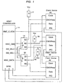
- the host controller 11 is a microprocessor module such as the Intel® PXA250 Microprocessor MMC Controller. It should be understood that this particular controller unit is described here by way of example only. Other processors, such as the Qualcomm® MSM6500 devices, can be used.
- the host controller 11 communicates with three devices, labeled client devices #1, #2, #3.
- One or more of the client devices may be part of the PDA itself, or may reside on an SD card.
- one of the client devices comprises an SD card slot and SD card containing an SDIO function.
- the SD card containing the SDIO function may also have another function, for example, a large memory.
- client device #1 may be the SD memory
- client device #2 may be the SDIO
- client device #3 may be a multi-media memory, MMC. All three client devices may reside on one or more SD cards, or one or more client devices may be part of the PDA. It should be apparent that three client devices are chosen by way of example. Any number of two or more client devices may be used for the invention.
- the client devices are interconnected to controller 11 through switching devices 14, 15.
- the switches are SP3T switches as shown.
- the simultaneous multiple functions are implemented with a 1-bit bus for controller 11.
- the Intel processor referred to above has a 1-bit bus for each of the MMC/SD/SDIO functions. It also has a 4-bit star bus for the SD memory and the SDIO functions. A four-bit bus implementation of the invention is also contemplated, and will be mentioned again below.
- Controller 11 has one dedicated command signal MMC_CMD, and one dedicated data signal MMC_DATA, which limits this specific configuration to the 1-bit bus implementation.
- the command, MMC_CMD transmits commands and receives responses from each of the client devices over lines that are multiplexed through switches 14, 15 to the MMC_CMD port on controller 11.
- the data signals from all three client devices are transmitted in sequential time slots through switches 14, 15, to the MMC_DATA port on controller 11.
- the time slots for data transmission are synchronized by MMC_CLOCK, which is connected to all three client devices.
- the GPIO ports on the controller are configured as interrupts for the three clients devices, and connected to the IRQ signals (usually through the CD and WP contacts on the card socket) on the three device cards.
- the switch selection lines SW_SELO, SW_SEL1 select the client devices for connection to the host controller.
- the MMC_CMD and MMC_DATA ports of the host controller are connected to client device #1. If client device #1 is operating, data is exchanged between client device #1 and the host processor. When the data transaction for client device #1 is finished, switches 14 and 15 are reset to interconnect client device #2 with the host controller. Data is then exchanged between client device #2 and the host controller. Similarly, data is exchanged between client device #3 and the host controller. Interrupt signals from the IRQ ports of the client devices indicate which client devices are active.
- the CMD/Resp lines from the client devices need to be high to avoid misreading a low voltage condition as a starting bit of a command signal.
- Pull-up resistors 17 on the CMD/Resp lines overcome this problem.
- the MMC/SD device driver on the host processor operates the switch select ports and the switches 14, 15, to connect the client devices between the command/response and data transfer/acknowledgement transaction.
- This enables the MMC/SD/SDIO port sessions between the host and the different client devices to occur essentially concurrently, and the user will see virtually simultaneous operation of the multiple client devices.
- This is possible since the MMC/SD/SDIO specifications require that the transmission from the client devices be initiated by the host. This makes it possible for the host to know when and what type of transmission (response, data, and acknowledgement) will be performed by the client device and allows the controller to wait until such transmission is complete before switching to a different client device.
- the CLOCK line is disabled at the LOW level and the CMD lines on the host and all client devices are pulled to logic level HIGH.
- the multiple MMC/SD/SDIO client devices can operate virtually simultaneously, sharing the bandwidth available on the host MMC/SD/SDIO controller.
- all multiplex switching is initiated by the host controller in response to CMD/Response signals from the client devices.
- the invention is easily implemented by adding switching elements to the additional three lines.
- the interrupt on the GPIO pins connected to the IRQ pin of the client devices should be disabled when the client device is switched in (connected to the host controller), and should be enabled when the client device is switched out (disconnected from the host controller).
- the GPIO interrupts may be enabled all the time during power up of the client devices.
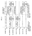
- FIG. 2 A time slot diagram showing operation of an SDIO client device (802.11 b WLAN module) and an external SD card is shown in Fig. 2 .
- the host controller sends a command and receives data from the client device #1, in this example the SDIO device.
- the controller then activates switches 14 and 15 to switch from the B1 positions to the B2 positions and interconnect client device #2, in this example an external SD card.
- the host processor sends commands and receives data from the SD card.
- the duration of the interchange transaction is indicated here as seven clock cycles but, as indicated earlier, since the controller controls both send and receive from each client device, the transactions may be longer or shorter. Switching from one client device to another, on the time scale implied above, is referred to as multiplexing, that is, transactions are multiplexed.
- the term "transaction", as used here, is well known in the PDA art.
- Figs. 1 and 2 are given by way of example only of the large number of circuit and software alternatives made possible using the simultaneous multiple function teachings of the invention.
- PDA device as used herein means a portable device, usually a hand-held device, and includes computers, cameras, cellphones, etc.
- PDA-SD device is a PDA device with at least one SD slot.
- Functional devices as used herein means devices that provide independent functions such as voice communications, wireless interface, images, video, general-purpose memory, etc.
- a combination of functional devices means any combination of the above provided as separate devices in a PDA, separate SD cards, combinations in a PDA and combinations on a single SD card, or provided by another interconnected device, e.g. a plug-in accessory device (not a card). Where two or more functions are built into a single SD card or other plug-in, the two or more functions are considered independent functions.
- Switching matrix means a combination of at least two switching elements, each of the elements having 1xn switching capability, where n is the number of functional devices served by the host controller.
Landscapes
- Engineering & Computer Science (AREA)
- Theoretical Computer Science (AREA)
- Physics & Mathematics (AREA)
- General Engineering & Computer Science (AREA)
- General Physics & Mathematics (AREA)
- Computer Hardware Design (AREA)
- Mathematical Physics (AREA)
- Computing Systems (AREA)
- Small-Scale Networks (AREA)
- Information Transfer Systems (AREA)
- Electrotherapy Devices (AREA)
Description
- This invention relates to implementing multiple functions with a single host controller, wherein the multiple functions are simultaneously active.
- Portable and wireless computer devices, such as PDAs, personal PCs, smart cell phones, etc. are becoming ubiquitous. For convenience, these devices are generically referred to here as PDAs. Many of these devices are equipped with SD slots to accommodate active integrated circuit cards. A common SD function is a memory function, and the cards may be any of a variety of memory cards. For example, one type of SD memory card is a multi-media card, or MMC, implemented using MMC circuits in the PDA. PDA units with WLAN wireless capability have SDIO interface circuits, and use SDIO cards. These provide the PDA with a wireless connection to a WLAN network. The SDIO card in this case carries an RF integrated circuit. The card may also have digital memory circuits to implement other SD functions. Other devices also use SD technology. Many digital cameras are provided with SD slots for SD memory cards. The SD card functions as the image storage medium. In these devices the memory circuit in the card may be very large, to allow many pictures to be stored. Cell phones may also be provided with SDIO capability. These are often referred to as Smartphones. In many of these prior art devices, the PDAs have a single SD function and have dedicated controller units to manage and switch data for the single function.
- Recent advances in PDA design and functionality allow more than one function to be accommodated in one PDA device. In these PDAs, a microprocessor host controller is designed to be switched by the user between functions, and to organize and distribute data in response to commands by the user. For example, Intel® PXA250 Microprocessor MMC Controller, originally designed as a single function (MMC) controller, now supports MMC/SD/SDIO functions. See Intel Application Note 278533-001, February 2002.
- A multi-function PDA device may employ a single SD slot, with a separate card for each function. Or it may use cards that contain more than one function. An especially useful multi-function card contains an SDIO function for WLAN communication. See for example
United States Patent No. 7,170,754 . - In the multi-function PDAs of the prior art, the microprocessors are designed to switch between functions depending on the needs of the user. Thus the multiple functions, while they may present a very large variety for the user, are available only one at a time.
-
US 2003/110342 discloses a technique for routing an enhanced USB device to an unoccupied enhanced USB transceiver. - The invention provides a PDA-SD device with multiple functions according to
claim 1. The invention further provides a method for concurrently operating a PDA device according toclaim 1. - We have recognized a need for a PDA device, and a PDA microprocessor controller, that allows simultaneous operation of multiple functions. A multiple function PDA is especially desirable when one of the multiple functions is a SDIO function. This capability extends the versatility of PDA devices into new dimensions. For example, in the case of a digital camera, the state of the art allows images that are stored in the MMC to be transmitted to a remote station using a wireless SDIO function. According to the invention, the MMC and SDIO functions may be activated simultaneously, allowing the images to be transmitted in virtual real time. Thus a digital camera may transmit images as they are taken. A simple buffer memory can replace or supplement the use of a large MMC. This is but one example of the versatility provided by simultaneously operating multiple functions.
- Simultaneous multiple functions are implemented by connecting all of the functional devices to the host controller, and multiplexing the command signals and the content data to and from the host controller to the individual devices. The interconnection may be implemented using a dynamic switching matrix that allows the host controller to switch from one functional device to another using signal responses from the functional devices.
-
-
Fig. 1 is a diagram showing one circuit embodiment for implementing the invention; -
Fig. 2 is a schedule of software commands for operating the circuit ofFig. 1 . - With reference to
Fig. 1 , thehost controller 11 is a microprocessor module such as the Intel® PXA250 Microprocessor MMC Controller. It should be understood that this particular controller unit is described here by way of example only. Other processors, such as the Qualcomm® MSM6500 devices, can be used. In the example shown inFig. 1 , thehost controller 11 communicates with three devices, labeledclient devices # 1, #2, #3. One or more of the client devices may be part of the PDA itself, or may reside on an SD card. In a preferred case, one of the client devices comprises an SD card slot and SD card containing an SDIO function. The SD card containing the SDIO function may also have another function, for example, a large memory. Thusclient device # 1 may be the SD memory, andclient device # 2 may be the SDIO.Client device # 3 may be a multi-media memory, MMC. All three client devices may reside on one or more SD cards, or one or more client devices may be part of the PDA. It should be apparent that three client devices are chosen by way of example. Any number of two or more client devices may be used for the invention. - The client devices are interconnected to controller 11 through switching
devices - Also in the example illustrated here, the simultaneous multiple functions are implemented with a 1-bit bus for
controller 11. The Intel processor referred to above has a 1-bit bus for each of the MMC/SD/SDIO functions. It also has a 4-bit star bus for the SD memory and the SDIO functions. A four-bit bus implementation of the invention is also contemplated, and will be mentioned again below. -
Controller 11 has one dedicated command signal MMC_CMD, and one dedicated data signal MMC_DATA, which limits this specific configuration to the 1-bit bus implementation. The command, MMC_CMD, transmits commands and receives responses from each of the client devices over lines that are multiplexed throughswitches controller 11. Likewise the data signals from all three client devices are transmitted in sequential time slots throughswitches controller 11. The time slots for data transmission, are synchronized by MMC_CLOCK, which is connected to all three client devices. - The GPIO ports on the controller are configured as interrupts for the three clients devices, and connected to the IRQ signals (usually through the CD and WP contacts on the card socket) on the three device cards.
- In operation, the switch selection lines SW_SELO, SW_SEL1 select the client devices for connection to the host controller. In the switch configuration shown the MMC_CMD and MMC_DATA ports of the host controller are connected to
client device # 1. Ifclient device # 1 is operating, data is exchanged betweenclient device # 1 and the host processor. When the data transaction forclient device # 1 is finished, switches 14 and 15 are reset to interconnectclient device # 2 with the host controller. Data is then exchanged betweenclient device # 2 and the host controller. Similarly, data is exchanged betweenclient device # 3 and the host controller. Interrupt signals from the IRQ ports of the client devices indicate which client devices are active. During the clock sequence when a given client device is not connected throughswitches resistors 17 on the CMD/Resp lines overcome this problem. - As will be understood from
Fig. 1 , the MMC/SD device driver on the host processor operates the switch select ports and theswitches - If the host controller is provided with 4-bit bus capability for the command and data ports, and the controller thus has four lines for these functions, the invention is easily implemented by adding switching elements to the additional three lines. In 4-bit operation of the SDIO client device, the interrupt on the GPIO pins connected to the IRQ pin of the client devices should be disabled when the client device is switched in (connected to the host controller), and should be enabled when the client device is switched out (disconnected from the host controller). In the 1-bit SDIO mode, the GPIO interrupts may be enabled all the time during power up of the client devices.
- A time slot diagram showing operation of an SDIO client device (802.11 b WLAN module) and an external SD card is shown in
Fig. 2 . During the first seven clock cycles shown, the host controller sends a command and receives data from theclient device # 1, in this example the SDIO device. The controller then activatesswitches client device # 2, in this example an external SD card. The host processor sends commands and receives data from the SD card. The duration of the interchange transaction is indicated here as seven clock cycles but, as indicated earlier, since the controller controls both send and receive from each client device, the transactions may be longer or shorter. Switching from one client device to another, on the time scale implied above, is referred to as multiplexing, that is, transactions are multiplexed. The term "transaction", as used here, is well known in the PDA art. -
Figs. 1 and2 are given by way of example only of the large number of circuit and software alternatives made possible using the simultaneous multiple function teachings of the invention. - PDA device as used herein means a portable device, usually a hand-held device, and includes computers, cameras, cellphones, etc. PDA-SD device is a PDA device with at least one SD slot.
- Functional devices as used herein means devices that provide independent functions such as voice communications, wireless interface, images, video, general-purpose memory, etc. A combination of functional devices means any combination of the above provided as separate devices in a PDA, separate SD cards, combinations in a PDA and combinations on a single SD card, or provided by another interconnected device, e.g. a plug-in accessory device (not a card). Where two or more functions are built into a single SD card or other plug-in, the two or more functions are considered independent functions.
- Switching matrix means a combination of at least two switching elements, each of the elements having 1xn switching capability, where n is the number of functional devices served by the host controller.
- Various additional modifications of this invention will occur to those skilled in the art. All deviations from the specific teachings of this specification that basically rely on the principles and their equivalents through which the art has been advanced are properly considered within the scope of the invention as described and claimed.
Claims (17)
- PDA-SD device with multiple (n) functions comprising:a. a host controller (11);b. at least two functional devices (#1, #2) in the PDA-SD device wherein one of the at least two functional devices is an SD card slot,c. a switching matrix comprising at least two 1xn switching elements (14, 15), the switching elements having a 1x node and at least two xn nodes, with the 1x nodes of the switches connected to the host controller, and one xn node connected to a functional device and another xn node connected to the SD card slot respectively, the switching matrix being activated by command signals from the host controller, andwherein each functional device has an information request port (IRQ), the host controller has multiple general purpose IO ports (GPIO) and each information request port is connected to a separate general purpose IO port.
- The device of claim 1 further including at least one additional SD card slot connected to the switching matrix.
- The device of claim 2 wherein the SD card slot is an SDIO card slot.
- The device of claim 1 wherein the switching matrix comprises a single pole multiple throw switch.
- The device of claim 1 wherein the host controller is an MMC/SD/SDIO controller.
- The device of claim 3 wherein each functional device has a data port (Data), and the data port is connected to the host controller through the switching matrix.
- The device of claim 6 wherein the data port of the SDIO device comprises a 1-bit data bus.
- The device of claim 6 wherein the data port of the SDIO device comprises a 4-bit data bus.
- The device of claim 6 wherein each functional device has a command/response port (CMD/Resp), and the command response port is connected to the host controller through the switching matrix.
- A method for concurrently operating a PDA device according to claim 1, comprising a first functional device (#1) and a second functional device (#2), wherein the functional devices have command/response ports (CMD/Resp), the method comprising:establishing a command/response connection between the command/response port of the first functional device and the host controller,conducting a transaction between the first functional device and the host controller,switching the command/response connection to the second functional device;connecting an information request port on each functional device to a separate general purpose IO port on the host controller; andconducting a transaction between the second functional device and the host controller.
- The method of claim 10 wherein the functional devices each have data ports (Data), and at least one transaction includes transmitting data between the functional devices and the host controller.
- The method of claim 11 wherein one of the functional devices comprises an SD card slot.
- The method of claim 11 wherein two functional devices comprise SD card slots.
- The method of claim 12 wherein an SD card slot comprises an SDIO card slot.
- The method of claim 10 wherein the host controller is an MMC/SD/SDIO controller.
- The method of claim 14 wherein the SDIO card slot comprises a 1-bit data bus.
- The method of claim 14 wherein the SDIO card slot comprises a 4-bit data bus.
Applications Claiming Priority (1)
| Application Number | Priority Date | Filing Date | Title |
|---|---|---|---|
| US10/885,941 US7269669B2 (en) | 2004-07-07 | 2004-07-07 | Sharing single host controller with multiple functional devices |
Publications (3)
| Publication Number | Publication Date |
|---|---|
| EP1615135A2 EP1615135A2 (en) | 2006-01-11 |
| EP1615135A3 EP1615135A3 (en) | 2006-04-12 |
| EP1615135B1 true EP1615135B1 (en) | 2012-02-01 |
Family
ID=35197764
Family Applications (1)
| Application Number | Title | Priority Date | Filing Date |
|---|---|---|---|
| EP05254141A Not-in-force EP1615135B1 (en) | 2004-07-07 | 2005-06-30 | Sharing single host controller with multiple functional devices |
Country Status (5)
| Country | Link |
|---|---|
| US (1) | US7269669B2 (en) |
| EP (1) | EP1615135B1 (en) |
| JP (1) | JP2006024217A (en) |
| KR (1) | KR101237763B1 (en) |
| CN (1) | CN1773474B (en) |
Cited By (1)
| Publication number | Priority date | Publication date | Assignee | Title |
|---|---|---|---|---|
| US9626112B2 (en) | 2014-12-08 | 2017-04-18 | Symbol Technologies, Llc | eMMC functionality expander |
Families Citing this family (23)
| Publication number | Priority date | Publication date | Assignee | Title |
|---|---|---|---|---|
| WO2007041834A1 (en) | 2005-10-07 | 2007-04-19 | Memory Experts International Inc. | Method and apparatus for secure credential entry without physical entry |
| JP4725725B2 (en) * | 2005-11-30 | 2011-07-13 | セイコーエプソン株式会社 | Information processing system and host device |
| US20070233954A1 (en) * | 2005-12-06 | 2007-10-04 | O2Micro, Inc. | System and Method for Interfacing to a Media Card Related Application and Technical Field |
| US20070299929A1 (en) * | 2006-06-27 | 2007-12-27 | Nielsen Stig S | Client device interface for portable communication devices |
| CN101136000B (en) * | 2006-09-01 | 2011-01-05 | 飞思卡尔半导体公司 | Application processor circuit for realizing SD host slave equipment and electronic equipments thererof |
| US7587544B2 (en) * | 2006-09-26 | 2009-09-08 | Intel Corporation | Extending secure digital input output capability on a controller bus |
| US8127309B1 (en) | 2006-11-10 | 2012-02-28 | Marvell International Ltd. | Secure digital input/output interface system |
| JP2009054103A (en) * | 2007-08-29 | 2009-03-12 | Panasonic Corp | Host apparatus for controlling multiple memory cards |
| JP5166922B2 (en) * | 2008-03-10 | 2013-03-21 | キヤノン株式会社 | Shared bus control device and control method thereof |
| TW201005529A (en) * | 2008-07-24 | 2010-02-01 | Jmicron Technology Corp | Method and system for dynamical managing removable device |
| CN102197404A (en) * | 2008-10-24 | 2011-09-21 | 松下电器产业株式会社 | Card host LSI, and set equipment possessing same |
| JP2012515959A (en) | 2009-01-21 | 2012-07-12 | イメイション・コーポレイション | Removable memory storage device having multiple authentication processing function |
| US20100205355A1 (en) * | 2009-02-11 | 2010-08-12 | Memory Experts International Inc. | Multiplexing secure digital memory |
| US7970976B2 (en) * | 2009-03-01 | 2011-06-28 | Qualcomm Incorporated | Remote memory access using reversible host/client interface |
| KR20110116710A (en) * | 2010-04-20 | 2011-10-26 | 삼성전자주식회사 | Apparatus and method for supporting a plurality of exterior memory in portable terminal |
| CN101835282B (en) * | 2010-04-23 | 2012-11-07 | 华为终端有限公司 | Wireless Internet access module, user terminal, secure digital card and wireless communication method |
| US8364870B2 (en) | 2010-09-30 | 2013-01-29 | Cypress Semiconductor Corporation | USB port connected to multiple USB compliant devices |
| US9432446B2 (en) | 2011-04-19 | 2016-08-30 | Ineda Systems Pvt. Ltd | Secure digital host controller virtualization |
| US9098259B1 (en) * | 2011-05-26 | 2015-08-04 | Amazon Technologies, Inc. | Secure digital input/output low-power mode |
| US20130042063A1 (en) * | 2011-08-08 | 2013-02-14 | Chi Mei Communication Systems, Inc. | System and method for controlling dual memory cards |
| CN102929749A (en) * | 2011-08-09 | 2013-02-13 | 中兴通讯股份有限公司 | Method and device for switching storage element and extension element on mobile terminal |
| CN105068952A (en) * | 2015-08-03 | 2015-11-18 | 浪潮(北京)电子信息产业有限公司 | SD interface multiplexing apparatus and method and electronic device |
| US11809247B2 (en) * | 2021-11-11 | 2023-11-07 | Getac Technology Corporation | Electronic device with connector supporting multiple connection standards and signal switching method and power supply method thereof |
Family Cites Families (17)
| Publication number | Priority date | Publication date | Assignee | Title |
|---|---|---|---|---|
| JPS6022266A (en) * | 1983-07-19 | 1985-02-04 | Nec Corp | Multiprocessor coupling system |
| JPH0816893B2 (en) * | 1986-03-11 | 1996-02-21 | キヤノン株式会社 | Communications system |
| CN86208050U (en) * | 1986-10-09 | 1987-09-16 | 程显超 | Signalkey-controlled switch for microcomputer |
| JPS6455682A (en) * | 1987-08-26 | 1989-03-02 | Matsushita Electric Ind Co Ltd | Card device |
| US5677864A (en) * | 1993-03-23 | 1997-10-14 | Chung; David Siu Fu | Intelligent memory architecture |
| US5841424A (en) * | 1997-03-03 | 1998-11-24 | Lextron Systems, Inc. | USB to multiple connect and support bays for peripheral devices |
| US6279114B1 (en) * | 1998-11-04 | 2001-08-21 | Sandisk Corporation | Voltage negotiation in a single host multiple cards system |
| US6600739B1 (en) * | 1999-06-07 | 2003-07-29 | Hughes Electronics Corporation | Method and apparatus for switching among a plurality of universal serial bus host devices |
| US6820148B1 (en) * | 2000-08-17 | 2004-11-16 | Sandisk Corporation | Multiple removable non-volatile memory cards serially communicating with a host |
| US6671748B1 (en) * | 2001-07-11 | 2003-12-30 | Advanced Micro Devices, Inc. | Method and apparatus for passing device configuration information to a shared controller |
| JP2003030127A (en) * | 2001-07-19 | 2003-01-31 | Toshiba Microelectronics Corp | Sdio host controller |
| US7136379B2 (en) * | 2001-10-10 | 2006-11-14 | Qualcomm Incorporated | Multiple-interface port multiplexer |
| TW538364B (en) * | 2001-12-10 | 2003-06-21 | Via Tech Inc | USB control circuit capable of automatically switching paths |
| US20030140129A1 (en) * | 2002-01-24 | 2003-07-24 | Noam Livnat | Installing communication protocol in a handheld device |
| JP3916060B2 (en) * | 2002-06-12 | 2007-05-16 | 日本ビクター株式会社 | Serial communication device |
| JP4024123B2 (en) * | 2002-10-10 | 2007-12-19 | 株式会社リコー | Memory card control method and electronic device |
| US20050144385A1 (en) * | 2003-12-30 | 2005-06-30 | Mowery Keith R. | Interfacing multiple flash memory cards to a computer system |
-
2004
- 2004-07-07 US US10/885,941 patent/US7269669B2/en not_active Expired - Fee Related
-
2005
- 2005-06-30 EP EP05254141A patent/EP1615135B1/en not_active Not-in-force
- 2005-07-07 JP JP2005198397A patent/JP2006024217A/en active Pending
- 2005-07-07 KR KR1020050061204A patent/KR101237763B1/en not_active IP Right Cessation
- 2005-07-07 CN CN2005100832564A patent/CN1773474B/en not_active Expired - Fee Related
Cited By (1)
| Publication number | Priority date | Publication date | Assignee | Title |
|---|---|---|---|---|
| US9626112B2 (en) | 2014-12-08 | 2017-04-18 | Symbol Technologies, Llc | eMMC functionality expander |
Also Published As
| Publication number | Publication date |
|---|---|
| KR20060049925A (en) | 2006-05-19 |
| JP2006024217A (en) | 2006-01-26 |
| KR101237763B1 (en) | 2013-02-28 |
| US20060010266A1 (en) | 2006-01-12 |
| CN1773474A (en) | 2006-05-17 |
| EP1615135A2 (en) | 2006-01-11 |
| CN1773474B (en) | 2010-11-17 |
| US7269669B2 (en) | 2007-09-11 |
| EP1615135A3 (en) | 2006-04-12 |
Similar Documents
| Publication | Publication Date | Title |
|---|---|---|
| EP1615135B1 (en) | Sharing single host controller with multiple functional devices | |
| TWI293216B (en) | Interface integrated circuit device for a usb connection | |
| US20060106962A1 (en) | USB On-The-Go implementation | |
| JP6400714B2 (en) | Flexible mobile device connectivity with automotive systems with USB hubs | |
| EP2504766B1 (en) | Configurable connector for system-level communication | |
| CA2443790C (en) | Communication interface for an electronic device | |
| US7725638B2 (en) | Application processor circuit incorporating both SD host and slave functions and electronic device including same | |
| US20010034807A1 (en) | Mobile communication terminal device | |
| CN201541285U (en) | Switching circuit for phone camera | |
| CN101236544B (en) | Method and device for multiple USB master device for sharing USB slave device | |
| US20090268743A1 (en) | Data transmission bridge device and control chip thereof for transmitting data | |
| JP2018073392A (en) | Flexible mobile device connectivity to automotive systems with usb hubs | |
| US20050060490A1 (en) | Apparatus for multiple host access to storage medium | |
| WO2014023247A1 (en) | Embedded device and method for control data communication based on the device | |
| US20050091437A1 (en) | Multi-function universal serial bus wireless bridge | |
| CN113641610A (en) | Processor interface circuit, time-sharing multiplexing method of processor interface and electronic equipment | |
| CN102144262B (en) | Memory card adapter | |
| CN101155364B (en) | Method for extending memory in mobile phone terminal | |
| WO2011015536A1 (en) | Electronic circuit for interconnecting a smartcard chip | |
| CN112199312A (en) | Interface conversion device of communication equipment and communication system | |
| EP1422628B1 (en) | Host apparatus, electronic device, and transmission system control method | |
| US20040049611A1 (en) | Flexible serial port configuration and method | |
| CN109586755B (en) | Communication device, communication storage device, switching method and terminal equipment | |
| CN212515793U (en) | USB high-speed serial port card | |
| CN110955629B (en) | Computing device |
Legal Events
| Date | Code | Title | Description |
|---|---|---|---|
| PUAI | Public reference made under article 153(3) epc to a published international application that has entered the european phase |
Free format text: ORIGINAL CODE: 0009012 |
|
| AK | Designated contracting states |
Kind code of ref document: A2 Designated state(s): AT BE BG CH CY CZ DE DK EE ES FI FR GB GR HU IE IS IT LI LT LU MC NL PL PT RO SE SI SK TR |
|
| AX | Request for extension of the european patent |
Extension state: AL BA HR LV MK YU |
|
| PUAL | Search report despatched |
Free format text: ORIGINAL CODE: 0009013 |
|
| AK | Designated contracting states |
Kind code of ref document: A3 Designated state(s): AT BE BG CH CY CZ DE DK EE ES FI FR GB GR HU IE IS IT LI LT LU MC NL PL PT RO SE SI SK TR |
|
| AX | Request for extension of the european patent |
Extension state: AL BA HR LV MK YU |
|
| 17P | Request for examination filed |
Effective date: 20060914 |
|
| AKX | Designation fees paid |
Designated state(s): DE FR GB |
|
| 17Q | First examination report despatched |
Effective date: 20070822 |
|
| GRAP | Despatch of communication of intention to grant a patent |
Free format text: ORIGINAL CODE: EPIDOSNIGR1 |
|
| GRAS | Grant fee paid |
Free format text: ORIGINAL CODE: EPIDOSNIGR3 |
|
| GRAA | (expected) grant |
Free format text: ORIGINAL CODE: 0009210 |
|
| AK | Designated contracting states |
Kind code of ref document: B1 Designated state(s): DE FR GB |
|
| REG | Reference to a national code |
Ref country code: GB Ref legal event code: FG4D |
|
| REG | Reference to a national code |
Ref country code: DE Ref legal event code: R096 Ref document number: 602005032482 Country of ref document: DE Effective date: 20120329 |
|
| PLBE | No opposition filed within time limit |
Free format text: ORIGINAL CODE: 0009261 |
|
| STAA | Information on the status of an ep patent application or granted ep patent |
Free format text: STATUS: NO OPPOSITION FILED WITHIN TIME LIMIT |
|
| 26N | No opposition filed |
Effective date: 20121105 |
|
| GBPC | Gb: european patent ceased through non-payment of renewal fee |
Effective date: 20120630 |
|
| REG | Reference to a national code |
Ref country code: DE Ref legal event code: R097 Ref document number: 602005032482 Country of ref document: DE Effective date: 20121105 |
|
| REG | Reference to a national code |
Ref country code: FR Ref legal event code: ST Effective date: 20130228 |
|
| PG25 | Lapsed in a contracting state [announced via postgrant information from national office to epo] |
Ref country code: GB Free format text: LAPSE BECAUSE OF NON-PAYMENT OF DUE FEES Effective date: 20120630 Ref country code: FR Free format text: LAPSE BECAUSE OF NON-PAYMENT OF DUE FEES Effective date: 20120702 |
|
| PGFP | Annual fee paid to national office [announced via postgrant information from national office to epo] |
Ref country code: DE Payment date: 20140625 Year of fee payment: 10 |
|
| REG | Reference to a national code |
Ref country code: DE Ref legal event code: R119 Ref document number: 602005032482 Country of ref document: DE |
|
| PG25 | Lapsed in a contracting state [announced via postgrant information from national office to epo] |
Ref country code: DE Free format text: LAPSE BECAUSE OF NON-PAYMENT OF DUE FEES Effective date: 20160101 |