EP0076098A2 - Key storage error processing system - Google Patents
Key storage error processing system Download PDFInfo
- Publication number
- EP0076098A2 EP0076098A2 EP82305012A EP82305012A EP0076098A2 EP 0076098 A2 EP0076098 A2 EP 0076098A2 EP 82305012 A EP82305012 A EP 82305012A EP 82305012 A EP82305012 A EP 82305012A EP 0076098 A2 EP0076098 A2 EP 0076098A2
- Authority
- EP
- European Patent Office
- Prior art keywords
- bit
- main storage
- key
- parity
- error
- Prior art date
- Legal status (The legal status is an assumption and is not a legal conclusion. Google has not performed a legal analysis and makes no representation as to the accuracy of the status listed.)
- Granted
Links
Images


Classifications
-
- G—PHYSICS
- G06—COMPUTING; CALCULATING OR COUNTING
- G06F—ELECTRIC DIGITAL DATA PROCESSING
- G06F3/00—Input arrangements for transferring data to be processed into a form capable of being handled by the computer; Output arrangements for transferring data from processing unit to output unit, e.g. interface arrangements
-
- G—PHYSICS
- G06—COMPUTING; CALCULATING OR COUNTING
- G06F—ELECTRIC DIGITAL DATA PROCESSING
- G06F12/00—Accessing, addressing or allocating within memory systems or architectures
- G06F12/14—Protection against unauthorised use of memory or access to memory
- G06F12/1458—Protection against unauthorised use of memory or access to memory by checking the subject access rights
- G06F12/1466—Key-lock mechanism
-
- G—PHYSICS
- G06—COMPUTING; CALCULATING OR COUNTING
- G06F—ELECTRIC DIGITAL DATA PROCESSING
- G06F11/00—Error detection; Error correction; Monitoring
- G06F11/07—Responding to the occurrence of a fault, e.g. fault tolerance
- G06F11/08—Error detection or correction by redundancy in data representation, e.g. by using checking codes
- G06F11/10—Adding special bits or symbols to the coded information, e.g. parity check, casting out 9's or 11's
- G06F11/1008—Adding special bits or symbols to the coded information, e.g. parity check, casting out 9's or 11's in individual solid state devices
-
- G—PHYSICS
- G06—COMPUTING; CALCULATING OR COUNTING
- G06F—ELECTRIC DIGITAL DATA PROCESSING
- G06F11/00—Error detection; Error correction; Monitoring
- G06F11/07—Responding to the occurrence of a fault, e.g. fault tolerance
- G06F11/08—Error detection or correction by redundancy in data representation, e.g. by using checking codes
- G06F11/10—Adding special bits or symbols to the coded information, e.g. parity check, casting out 9's or 11's
- G06F11/1076—Parity data used in redundant arrays of independent storages, e.g. in RAID systems
-
- G—PHYSICS
- G06—COMPUTING; CALCULATING OR COUNTING
- G06F—ELECTRIC DIGITAL DATA PROCESSING
- G06F12/00—Accessing, addressing or allocating within memory systems or architectures
- G06F12/02—Addressing or allocation; Relocation
- G06F12/08—Addressing or allocation; Relocation in hierarchically structured memory systems, e.g. virtual memory systems
- G06F12/12—Replacement control
- G06F12/121—Replacement control using replacement algorithms
- G06F12/126—Replacement control using replacement algorithms with special data handling, e.g. priority of data or instructions, handling errors or pinning
-
- G—PHYSICS
- G06—COMPUTING; CALCULATING OR COUNTING
- G06F—ELECTRIC DIGITAL DATA PROCESSING
- G06F2212/00—Indexing scheme relating to accessing, addressing or allocation within memory systems or architectures
- G06F2212/10—Providing a specific technical effect
- G06F2212/1032—Reliability improvement, data loss prevention, degraded operation etc
Definitions
- the present invention relates to a key storage error processing system.
- FIG. 1 of the accompanying drawings is a schematic diagram explanatory of the relationship between a main storage and a key storage.
- MS indicates generally a main storage; P designates pages; K indicates a main storage key; A denotes access-control bits; F is a fetch-protection bit; R is a reference bit; and C is a change bit.
- the main storage MS is split into a plurality of pages P, each consisting of a 2K-byte block, for instance, and associated with one main storage key K.
- the main storage key K is stored in a key storage (not shown).
- An information processing system equipped with such a main storage and such a key (key in) storage as mentioned above is disclosed, for example, in IBM System/370 Principles of Operation.
- the access-control bits A of the main storage key K are matched with a program-protection key, thereby to perform storage protection of the main storage MS.
- the fetch-protection bit F indicates whether storage protection is applied when information is fetched from the main storage MS.
- the reference bit R indicates whether the corresponding page of the main storage is accessed, and when the page is accessed, the reference bit R of the main storage key K corresponding to the page is set to a "1".
- the change bit C indicates whether information is stored in (has been stored into) the corresponding page of the main storage MS, and when information is (has been) stored into the page, the change bit C of the corresponding main storage key K is set to a "I".
- the reference bit R and the change bit C are used when information is transferred in units of pages, to the main storage MS from an external storage, such as a magnetic disc unit.
- an external storage such as a magnetic disc unit.
- information is fetched and stored on the assumption that a storage area of an external storage exists in the main storage. Accordingly, when required information is not in fact. present in the main storage MS, the information must be paged-in from the external storage to the main storage MS and an area must be secured therefor in the main storage MS. In this case, if there is no free or space area in the main storage MS, a search is made for an area of main storage holding information that is considered unnecessary and the information is paged-out into the external storage to secure an area for receiving the required information from the external storage.
- priorities are usually attached to the pages for making a search for an area holding unnecessary information.
- Figure 2 of the accompanying drawings is a schematic diagram which shows the relationship between the priority assigned or attached to a page and the reference and change bits R and C of the main storage key relating to the page.
- the change bit C is "O"
- the reference bit R indicates whether the page of the main storage MS corresponding to the main storage key K is accessed or not.
- the reference bit R and the change bit C are both "O"
- the contents of the corresponding page are not changed, nor is the page accessed, so that the page is given the highest priority for save.
- the reference bit R and the change bit C are both "1”
- the reference bit R is set to "0" by the execution of a reset reference bit instruction when the key storage is retrieved for a fixed period of time or for the page-out operation.
- FIG. 3 of the accompanying drawings is a schematic diagram explanatory of a conventional error processing system in a case in which odd parity is employed.
- FIG 3 shows a case in which two bits of a pair comprising the reference bit R or the change bit C and a parity bit are correct at a time tl; (b) shows a case in which when the reference bit R or the change bit C is read out at a time t2 after the lapse of an arbitrary period of time, one of the two bits is erroneous; and (c) shows a case in which the reference bit R or the change bit C is read out at a time t3 a certain period of time after the time t2, the other bit is also erroneous.
- an asterisk is used to indicate an erroneous bit.
- (1), (3), (5), and (7) each show a bit pair comprising a reference bit R or a change bit C and a parity bit
- (2), (4) (6) and (8) each show bits that are transferred to an access control unit of the main storage MS for making a decision on page-out and so on.
- a key storage error processing system for a system which is provided with a key storage having stored therein main storage keys respectively corresponding to pages into which a main storage is divided, each main storage key having at least a reference bit indicating whether the corresponding page has been accessed and a change bit indicating whether information has been written into the page;
- the present invention can provide a key storage error processing system which remedies errors in reference and update (change) bits of a key storage.
- An embodiment of the present invention can provide a key storage error processing system which performs correction processing at the time of detecting an error so as to prevent a system breakdown even by an error in key storage.
- An embodiment of thepresent invention can provide a key storage error processing system which performs correction processing, with a simple arrangement, for preventing reduction of system performances, and for preventing system breakdown, by the detection of an error in a reference bit or change bit of a main storage key.
- a parity bit is added to each of reference and change bits of the key and when the main storage key is read out a parity check takes place. If a parity error is detected the reference bit is set to a content indicating an access and the change bit is set to a content indicating a store (indicating that the page has been updated) and, further, a parity bit is added; and then the main storage key is rewritten.
- FIG 4 shows a case in which two bits (a bit pair) consisting of a reference bit R, or a change bit C, and a parity bit are correct at a time tl;
- (b) shows a case in which when the reference bit R, or the change bit C, is read out at the time t2, an error occurs in one of the two bits of the bit pair;
- (c) shows a case in which a rewrite is carried out at the time t3 because of a parity error; and
- (d) shows a case in which an error occurs in the other bit of the bit pair (the other bit as compared with (b) ) when the reference bit R, or the change bit C, is read out at a time t4 an arbitrary period of time after the time t3.
- the pair made up of the reference bit R, or the change bit C, and the parity bit is initially correct(at time t1) and the main storage key is read out at the time t2,if a parity error is then detected.- a "1" is transferred to the access control unit and, at the immediately subsequent time t3, the reference bit R is set to a "1" indicating an access to the corresponding page (or the change bit C is set to a "1" indicating a store in the page, updating of the page)and,further, a "0" parity bit is added to the reference bit (or to the change bit),which is followed by rewriting of the main storage key.
- This state is shown in (c) corresponding to the time t3. That is to say, when an error is detected by the parity check of the pair of the reference bit R, or the change bit C,,and the parity bit, a "1" is transferred to the access control unit and the reference bit R, or the change bit C, is set to a "1" and, at the same time, the parity bit is set to a "0" to provide a state in which the corresponding page is given a reduced priority for save, and then the main storage key is rewritten.
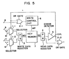
- Figure 5 illustrates in block form principal parts of apparatus in accordance with an embodiment of the present invention.
- 1-1 and 1-2 are selectors; 2-1 and 2-2 are OR gates; 3 is a write data register; 4 is a read data register; 5 is an error detector; 6 is a write control circuit; 7 is a key memory; 8 a write signal input terminal; 9 is a parity bit input terminal; 10 is an input terminal to which a "0" is fixedly applied; 11 is a reference bit input terminal; 12 is an input terminal to which a "1" is fixedly applied; RD is read data; WD is write data; ERR is an error detection signal; WP is write pulses; R is a reference bit; and P is a parity bit.
- Figure 5 there are shown only the parts associated with the reference bit of the main storage key; the change bit, other bits, the main storage, its access control units and so forth are .not shown for the sake of brevity.
- the read data RD is set in the read data register 4 and subjected to a parity check by the error detector 5 constituted by an exclusive NOR circuit or the like.
- the error detection signal ERR goes to "0".
- the selectors 1-1 and 1-2 select the parity bit and the reference bit from the input terminals 9 and 11.
- the reference bit is a bit that is input corresponding to the page of the main storage when the main storage is accessed, as described previously.
- the reference bit R is provided via the OR gate 2-2 to an access control unit not shown.
- the error detection signal ERR goes to "1".
- This "1” is transferred via the OR gate 2-2 to the access control unit. That is, when an error is detected, even if the reference bit R is a "O", "1" is provided to the access control unit on the assumption that the reference bit R is a "I”. And when the error detection signal ERR is "I”, the selectors 1-1 and 1-2 select the “0” and the "1” which are fixedly applied to the input terminals 10 and 12, respectively, and apply them to the write data register 3.
- the write control circuit 6 is started by a “k” ("1") which is applied thereto via the OR gate 2-1, and outputs the write pulses WP.
- the write pulses WP By the write pulses WP the contents of the write data register 3 are written into the key memory 7. In this case, since the contents of the write data register 3 are written into the same address as the address of the main storage key read out, the reference bit R and the parity bit P of the main storage key are written as "10". In other words, the reference bit R and the parity bit P are rewritten by the error detection into "10" as shown in (c) in Figure 4.
- bit pair comprising a change bit C and a parity bit is also rewritten by the error detection through an arrangement similar to that abovedescribed.
- the main storage key is rewritten with a reference bit value indicating that the page corresponding to the main storage key has been accessed (and a change bit value indicating that the page has been rewritten). Accordingly, the save priority of the relevant page of the main storage is not raised and a required page is not saved. Even if the page is saved, necessary data is not extinguished because the page-out operation is carried out without fail. Therefore, system breakdown can be avoided.
- each main storage key has at least a reference bit indicating whether the corresponding,page has been accessed and a change bit indicating whether information has been written in the corresponding page.
- a parity bit is added to each of the reference bit and the change bit to form the main storage key.
- detecting means for detecting a parity error in a pair consisting of the reference bit and its parity bit, and for detecting a parity error in a pair consisting of change bit and its parity bit, when the main storage key is read out.
Landscapes
- Engineering & Computer Science (AREA)
- Theoretical Computer Science (AREA)
- Physics & Mathematics (AREA)
- General Engineering & Computer Science (AREA)
- General Physics & Mathematics (AREA)
- Quality & Reliability (AREA)
- Computer Security & Cryptography (AREA)
- Human Computer Interaction (AREA)
- Storage Device Security (AREA)
- Techniques For Improving Reliability Of Storages (AREA)
- Memory System Of A Hierarchy Structure (AREA)
- Detection And Correction Of Errors (AREA)
Abstract
Description
- The present invention relates to a key storage error processing system.
- Figure 1 of the accompanying drawings is a schematic diagram explanatory of the relationship between a main storage and a key storage. In Figure 1, MS indicates generally a main storage; P designates pages; K indicates a main storage key; A denotes access-control bits; F is a fetch-protection bit; R is a reference bit; and C is a change bit. The main storage MS is split into a plurality of pages P, each consisting of a 2K-byte block, for instance, and associated with one main storage key K. The main storage key K is stored in a key storage (not shown). An information processing system equipped with such a main storage and such a key (key in) storage as mentioned above is disclosed, for example, in IBM System/370 Principles of Operation.
- Whenever information is stored or fetched, the access-control bits A of the main storage key K are matched with a program-protection key, thereby to perform storage protection of the main storage MS. The fetch-protection bit F indicates whether storage protection is applied when information is fetched from the main storage MS. The reference bit R indicates whether the corresponding page of the main storage is accessed, and when the page is accessed, the reference bit R of the main storage key K corresponding to the page is set to a "1". The change bit C indicates whether information is stored in (has been stored into) the corresponding page of the main storage MS, and when information is (has been) stored into the page, the change bit C of the corresponding main storage key K is set to a "I".
- The reference bit R and the change bit C are used when information is transferred in units of pages, to the main storage MS from an external storage, such as a magnetic disc unit. For instance, in a computer system having a virtual storage system, information is fetched and stored on the assumption that a storage area of an external storage exists in the main storage. Accordingly, when required information is not in fact. present in the main storage MS, the information must be paged-in from the external storage to the main storage MS and an area must be secured therefor in the main storage MS. In this case, if there is no free or space area in the main storage MS, a search is made for an area of main storage holding information that is considered unnecessary and the information is paged-out into the external storage to secure an area for receiving the required information from the external storage.
- In such a page-out operation, priorities are usually attached to the pages for making a search for an area holding unnecessary information.
- Figure 2 of the accompanying drawings is a schematic diagram which shows the relationship between the priority assigned or attached to a page and the reference and change bits R and C of the main storage key relating to the page. When the change bit C is "O", it indicates that the contents of the page of the main storage MS corresponding to the main storage key K remain unchanged and, accordingly, that the contents of the page are stored in the external storage and the contents of the page need not be transferred thereto. That is, a page-out operation is unnecessary. The reference bit R indicates whether the page of the main storage MS corresponding to the main storage key K is accessed or not. Accordingly, when the reference bit R and the change bit C are both "O", the contents of the corresponding page are not changed, nor is the page accessed, so that the page is given the highest priority for save. When the reference bit R and the change bit C are both "1", this indicates that the contents of the relevant page are changed and that the page is accessed and, accordingly, the page is given the fourth priority for save. Incidentally, the reference bit R is set to "0" by the execution of a reset reference bit instruction when the key storage is retrieved for a fixed period of time or for the page-out operation.
- It is general practice to add a parity bit for detecting an error in the reference bit R and the change bit C.
- Figure 3 of the accompanying drawings is a schematic diagram explanatory of a conventional error processing system in a case in which odd parity is employed.
- In Figure 3,(a) shows a case in which two bits of a pair comprising the reference bit R or the change bit C and a parity bit are correct at a time tl; (b) shows a case in which when the reference bit R or the change bit C is read out at a time t2 after the lapse of an arbitrary period of time, one of the two bits is erroneous; and (c) shows a case in which the reference bit R or the change bit C is read out at a time t3 a certain period of time after the time t2, the other bit is also erroneous. In Figure 3, an asterisk is used to indicate an erroneous bit. In Figure 3, (1), (3), (5), and (7) each show a bit pair comprising a reference bit R or a change bit C and a parity bit, and (2), (4) (6) and (8) each show bits that are transferred to an access control unit of the main storage MS for making a decision on page-out and so on.
- For instance, when the main storage key K is read out at the time tl as shown in (a)-(l) or (a)-(3),"01", which is a bit pair comprising a "0" reference bit R or change bit C and a "1" parity bit, is correct ands, consequently, a "0" as shown in (a)-(2) or (a)-(4) is transferred to the access control unit of the main storage MS. When readout takes place again at the subsequent time t2, if a one-bit error occurs which results in a bit pair "11" as shown in (b)-(1), the error is detected by a parity check and a "1" shown in (b)-(2) is transferred to the access control unit. That is, when an error is detected by the parity check, -a "1" indicating an access or a store is transferred to the access control unit. Further, when the other bit of a bit pair also becomes erroneous as at the time t3 to provide "10" as shown in (c)-(1), it is decided as error-free by the parity check and "1" shown in (c)-(2) is transferred to the access control unit. Also in the case where the main storage key K is read out at the time t2 and a one-bit error occurs to provide "00", a "1" shown in (b)-(4) is transferred to the access control unit. Moreover, when the other bit becomes erroneous to provide "10" as shown in (c)-(3), it is decided as error-free by the parity check and a "1" shown in (c)-(4) is in (c)-(4) is transferred to the access control unit.
- When the reference bit R is changed from a "0" to a "1", the priority for save of the page corresponding to the main storage key is reduced (as will be seen from Figure 2) and even if its priority is the first or second one, it is given the third or fourth priority. This merely reduces the number of pages of high priorities which are to be saved, but does not significantly impair the system performances. When the change bit C is changed from a "0" to a "1", the priority for save of the page is reduced as is the case with the reference bit (see Figure 2). Further, when the page corresponding to the main storage key is designated to be saved, a page-out operation takes place (when C="l"). This means that a page-out operation, which is omissible if the change bit C is a "O", is carried out, resulting in somewhat lowered system performances, but this does not matter so seriously.
- In a case in which the correct content of a bit pair is "10" as shown in (a)-(5), if the reference bit R or the change bit C becomes erroneous as shown in (b)-(5), a "1" shown in (b)-(6) is transferred to the access control unit as a result of a parity check. However, if the . content becomes "01" owing to an error of the other bit at the time of reading out the main storage key K at the time t3 as shown in (c)-(5), the content is decided as error-free by the parity check and a "0" shown in (c)-(6) is transferred to the access control unit. The same is true of the case where the content "10" of the bit pair at the time tl changes to "11": at the time t2 and then changes to "Ol" at the time t3 as shown in (7). In this way, a change in the reference bit R or the changsbit C increases the priority for save, and this introduces the possibility of saving a page which ought not to be saved. In consequence, there are some occasions when a page which may well be in use is paged-out and then paged-in, resulting in appreciably impaired system performance. Moreover, if the change bit C changes from a "1" to a "0" owing to an error, data rewritten on the main storage can be extinguished by the omission of the page-out operation. Accordingly, the system can break down in the worst case.
- According to the present invention there is provided a key storage error processing system for a system which is provided with a key storage having stored therein main storage keys respectively corresponding to pages into which a main storage is divided, each main storage key having at least a reference bit indicating whether the corresponding page has been accessed and a change bit indicating whether information has been written into the page;
- in which system:-
- respective parity bits are added to the reference bit and the change bit to form the main storage key;
- and which system comprises:-
- detecting means for detecting a parity error in a pair consisting of the reference bit concerned and its associated parity bit and a pair consisting of the change bit concerned and its associated parity bit, when a main storage key is read out; and
- means for rewriting the main storage key after setting the reference bit concerned to a value indicating that the corresponding page has been accessed and adding a new parity bit to the thus set reference bit, when a parity error is detected by the detecting means in the pair consisting of the reference bit concerned and its associated parity bit, and/or after setting the change bit concerned to a value indicating that the corresponding page has been written into and adding a new parity bit to the thus set change bit, when a parity error is detected in the pair consisting of the change bit concerned and its associated parity bit.
- The present invention can provide a key storage error processing system which remedies errors in reference and update (change) bits of a key storage.
- An embodiment of the present invention can provide a key storage error processing system which performs correction processing at the time of detecting an error so as to prevent a system breakdown even by an error in key storage.
- An embodiment of thepresent invention can provide a key storage error processing system which performs correction processing, with a simple arrangement, for preventing reduction of system performances, and for preventing system breakdown, by the detection of an error in a reference bit or change bit of a main storage key.
- Briefly, according to an embodiment of the present invention, in a system which has main .storage keys respectively corresponding to pages of a main storage, a parity bit is added to each of reference and change bits of the key and when the main storage key is read out a parity check takes place. If a parity error is detected the reference bit is set to a content indicating an access and the change bit is set to a content indicating a store (indicating that the page has been updated) and, further, a parity bit is added; and then the main storage key is rewritten.
- Reference is made, by way of example, to the accompanying drawings, in which:-
- Figure 1 is a schematic diagram explanatory of a main storage and a main storage key;
- Figure 2 is a schematic diagram explanatory of save priority;
- Figure 3 is a schematic diagram explanatory of a conventional error processing system;
- Figure 4 is a schematic diagram explanatory of an error processing system embodying the present invention; and
- Figure 5 is a block diagram illustrating apparatus in accordance with an embodiment of the present invention.
- In Figure 4, (a) shows a case in which two bits (a bit pair) consisting of a reference bit R, or a change bit C, and a parity bit are correct at a time tl; (b) shows a case in which when the reference bit R, or the change bit C, is read out at the time t2, an error occurs in one of the two bits of the bit pair; (c) shows a case in which a rewrite is carried out at the time t3 because of a parity error; and (d) shows a case in which an error occurs in the other bit of the bit pair (the other bit as compared with (b) ) when the reference bit R, or the change bit C, is read out at a time t4 an arbitrary period of time after the time t3. In Figure 4, an asterisk is used the bit in which an error has occurred. (1), (3), (5) and (7) show bit pairs each of a reference bit R or a change bit C and a parity bit, and (2), (4), (6) and (8) show bits that are transferred to an access control unit of the main storage MS for a decision on page-out and so on.
- According to an embodiment of the present invention, in a case in which the pair made up of the reference bit R, or the change bit C, and the parity bit is initially correct(at time t1) and the main storage key is read out at the time t2,if a parity error is then detected.- a "1" is transferred to the access control unit and, at the immediately subsequent time t3, the reference bit R is set to a "1" indicating an access to the corresponding page (or the change bit C is set to a "1" indicating a store in the page, updating of the page)and,further, a "0" parity bit is added to the reference bit (or to the change bit),which is followed by rewriting of the main storage key. This state is shown in (c) corresponding to the time t3. That is to say, when an error is detected by the parity check of the pair of the reference bit R, or the change bit C,,and the parity bit, a "1" is transferred to the access control unit and the reference bit R, or the change bit C, is set to a "1" and, at the same time, the parity bit is set to a "0" to provide a state in which the corresponding page is given a reduced priority for save, and then the main storage key is rewritten. Accordingly, even if an error occurs in another bit, different from the erroneous bit at the time t2, when the main storage key is read out at the time t4, a "1" is transferred to the access control unit of the main storage, reducing the priority for save. Furthermore, when the change bit C changes from a "1" to a "0" due to an error, page-out operation is not omitted even if the corresponding page is to be saved; therefore, the present invention exhibits an advantage over the prior art in that stored information on the main storage is not extinguished.
- For example, in the case where a pair consisting of a "1" reference bit R, or change bit C, and a "0" parity bit is "10" at the time tl as shown in (a)-(5), if it becomes "00" as shown in (b)-(5) when the main storage key is read out at the time t2, a "1" is transferred to the access control unit as shown in (b)-(6) and, at the time t3 immediately thereafter, the reference bit R, or the change bit C, is set to a "1" and the parity bit is set to a "O", and "10" is written as shown in (c)-(5). Assuming that the bit pair becomes "11" due to an error in one bit as shown in (d)-(5) when the main storage key is read out again at the time t4, the error is detected by a parity check and a "1" is transferred to the access control unit. Also in this case, "10" is written. Accordingly, even if the reference bit R or the change bit C changes from a "1" to a "0" owing to a bit error, and even if the parity bit changes from a "0" to a "1", the reference bit R or the change bit C is corrected to a "1" before rewriting. As a result of this, the priority for save is not raised and the page-out operation is not omitted, ensuring the prevention of system breakdown even if the page corresponding to the main storage key is has to be saved.
- Figure 5 illustrates in block form principal parts of apparatus in accordance with an embodiment of the present invention. In Figure 5, 1-1 and 1-2 are selectors; 2-1 and 2-2 are OR gates; 3 is a write data register; 4 is a read data register; 5 is an error detector; 6 is a write control circuit; 7 is a key memory; 8 a write signal input terminal; 9 is a parity bit input terminal; 10 is an input terminal to which a "0" is fixedly applied; 11 is a reference bit input terminal; 12 is an input terminal to which a "1" is fixedly applied; RD is read data; WD is write data; ERR is an error detection signal; WP is write pulses; R is a reference bit; and P is a parity bit. In Figure 5 there are shown only the parts associated with the reference bit of the main storage key; the change bit, other bits, the main storage, its access control units and so forth are .not shown for the sake of brevity.
- When the main storage key corresponding to one of the pages of the main storage is read out from the
key memory 7, the read data RD is set in the readdata register 4 and subjected to a parity check by theerror detector 5 constituted by an exclusive NOR circuit or the like. When the read data is determined to be error-free by the parity check, the error detection signal ERR goes to "0". When the error detection signal ERR is "0", the selectors 1-1 and 1-2 select the parity bit and the reference bit from theinput terminals 9 and 11. The reference bit is a bit that is input corresponding to the page of the main storage when the main storage is accessed, as described previously. Of the contents of the readdata register 4, the reference bit R is provided via the OR gate 2-2 to an access control unit not shown. - When an error is detected in the
error detector 5, the error detection signal ERR goes to "1". This "1" is transferred via the OR gate 2-2 to the access control unit. That is, when an error is detected, even if the reference bit R is a "O", "1" is provided to the access control unit on the assumption that the reference bit R is a "I". And when the error detection signal ERR is "I", the selectors 1-1 and 1-2 select the "0" and the "1" which are fixedly applied to theinput terminals write data register 3. Thewrite control circuit 6 is started by a "k" ("1") which is applied thereto via the OR gate 2-1, and outputs the write pulses WP. By the write pulses WP the contents of thewrite data register 3 are written into thekey memory 7. In this case, since the contents of thewrite data register 3 are written into the same address as the address of the main storage key read out, the reference bit R and the parity bit P of the main storage key are written as "10". In other words, the reference bit R and the parity bit P are rewritten by the error detection into "10" as shown in (c) in Figure 4. - Furthermore, a bit pair comprising a change bit C and a parity bit is also rewritten by the error detection through an arrangement similar to that abovedescribed.
- As has been described above, in an embodiment of the present invention, when a bit pair of a reference bit R, or a change bit C, and a parity bit are read out, if a parity error is detected, the main storage key is rewritten with a reference bit value indicating that the page corresponding to the main storage key has been accessed (and a change bit value indicating that the page has been rewritten). Accordingly, the save priority of the relevant page of the main storage is not raised and a required page is not saved. Even if the page is saved, necessary data is not extinguished because the page-out operation is carried out without fail. Therefore, system breakdown can be avoided.
- It will be apparent that many modifications and variations may be effected without departing from the scope of the novel concepts of the present invention.
- Thus, in an embodiment of this invention, in a system which is provided with a key storage having stored therein main storage keys respectively corresponding to pages into which a main storage is split, each main storage key has at least a reference bit indicating whether the corresponding,page has been accessed and a change bit indicating whether information has been written in the corresponding page. A parity bit is added to each of the reference bit and the change bit to form the main storage key. There are provided detecting means for detecting a parity error in a pair consisting of the reference bit and its parity bit, and for detecting a parity error in a pair consisting of change bit and its parity bit, when the main storage key is read out. There are also provided means for rewriting the main storage key after setting the reference bit to a "I" indicating that the corresponding page has been accessed, and after adding a new parity bit "O" to the reference bit, when a parity error is detected by the detecting means in the pair consisting of the reference bit and its parity bit, and/or after setting the change bit to a "1" indicating that the corresponding page has been written into, and after adding a new parity bit "0" to the change bit, when a parity error is detected in the pair consisting of the change bit and its parity bit, whereby to control the save of the pages of the main storage.
Claims (2)
Applications Claiming Priority (2)
| Application Number | Priority Date | Filing Date | Title |
|---|---|---|---|
| JP56151046A JPS5853097A (en) | 1981-09-24 | 1981-09-24 | Processing system for key storage error |
| JP151046/81 | 1981-09-24 |
Publications (3)
| Publication Number | Publication Date |
|---|---|
| EP0076098A2 true EP0076098A2 (en) | 1983-04-06 |
| EP0076098A3 EP0076098A3 (en) | 1984-10-03 |
| EP0076098B1 EP0076098B1 (en) | 1986-12-10 |
Family
ID=15510109
Family Applications (1)
| Application Number | Title | Priority Date | Filing Date |
|---|---|---|---|
| EP82305012A Expired EP0076098B1 (en) | 1981-09-24 | 1982-09-23 | Key storage error processing system |
Country Status (8)
| Country | Link |
|---|---|
| US (1) | US4514847A (en) |
| EP (1) | EP0076098B1 (en) |
| JP (1) | JPS5853097A (en) |
| KR (1) | KR860002027B1 (en) |
| AU (1) | AU537967B2 (en) |
| BR (1) | BR8205588A (en) |
| CA (1) | CA1183608A (en) |
| DE (1) | DE3274686D1 (en) |
Families Citing this family (4)
| Publication number | Priority date | Publication date | Assignee | Title |
|---|---|---|---|---|
| JPS62293599A (en) * | 1986-06-13 | 1987-12-21 | Hitachi Ltd | Semiconductor storage device |
| US5031179A (en) * | 1987-11-10 | 1991-07-09 | Canon Kabushiki Kaisha | Data communication apparatus |
| US4916703A (en) * | 1988-11-28 | 1990-04-10 | International Business Machines Corporation | Handling errors in the C bit of a storage key |
| JP3786993B2 (en) * | 1995-12-14 | 2006-06-21 | 株式会社日立製作所 | Data storage unit and data storage device using the unit |
Citations (3)
| Publication number | Priority date | Publication date | Assignee | Title |
|---|---|---|---|---|
| US4084236A (en) * | 1977-02-18 | 1978-04-11 | Honeywell Information Systems Inc. | Error detection and correction capability for a memory system |
| US4092713A (en) * | 1977-06-13 | 1978-05-30 | Sperry Rand Corporation | Post-write address word correction in cache memory system |
| EP0010123A2 (en) * | 1978-10-12 | 1980-04-30 | International Business Machines Corporation | Paging control store data processing apparatus |
Family Cites Families (4)
| Publication number | Priority date | Publication date | Assignee | Title |
|---|---|---|---|---|
| US4053752A (en) * | 1975-09-15 | 1977-10-11 | International Business Machines Corporation | Error recovery and control in a mass storage system |
| US4020459A (en) * | 1975-10-28 | 1977-04-26 | Bell Telephone Laboratories, Incorporated | Parity generation and bus matching arrangement for synchronized duplicated data processing units |
| US4146099A (en) * | 1976-08-17 | 1979-03-27 | Christopher Scientific Company | Signal recording method and apparatus |
| US4103823A (en) * | 1976-12-20 | 1978-08-01 | International Business Machines Corporation | Parity checking scheme for detecting word line failure in multiple byte arrays |
-
1981
- 1981-09-24 JP JP56151046A patent/JPS5853097A/en active Granted
-
1982
- 1982-09-15 AU AU88415/82A patent/AU537967B2/en not_active Ceased
- 1982-09-20 US US06/419,927 patent/US4514847A/en not_active Expired - Lifetime
- 1982-09-23 KR KR8204296A patent/KR860002027B1/en active
- 1982-09-23 EP EP82305012A patent/EP0076098B1/en not_active Expired
- 1982-09-23 DE DE8282305012T patent/DE3274686D1/en not_active Expired
- 1982-09-23 BR BR8205588A patent/BR8205588A/en not_active IP Right Cessation
- 1982-09-23 CA CA000412069A patent/CA1183608A/en not_active Expired
Patent Citations (3)
| Publication number | Priority date | Publication date | Assignee | Title |
|---|---|---|---|---|
| US4084236A (en) * | 1977-02-18 | 1978-04-11 | Honeywell Information Systems Inc. | Error detection and correction capability for a memory system |
| US4092713A (en) * | 1977-06-13 | 1978-05-30 | Sperry Rand Corporation | Post-write address word correction in cache memory system |
| EP0010123A2 (en) * | 1978-10-12 | 1980-04-30 | International Business Machines Corporation | Paging control store data processing apparatus |
Non-Patent Citations (3)
| Title |
|---|
| COMPUTER DESIGN, vol. 20, no. 7, July 1981, pages 151-156, Concord, US; P.D. VOGT: "Memory management" * |
| IBM TECHNICAL DISCLOSURE BULLETIN, vol. 14, no. 12, May 1972, pages 3584-3585, New York, US; R.S. CAPOWSKI et al.: "Storage protect mechanism with reference and change recording" * |
| IBM TECHNICAL DISCLOSURE BULLETIN, vol. 20, no. 9, February 1978, pages 3585-2586, New York, US; E.J. ANNUNZIATA et al.: "Cache error handling in a store-in-cache design" * |
Also Published As
| Publication number | Publication date |
|---|---|
| CA1183608A (en) | 1985-03-05 |
| KR860002027B1 (en) | 1986-11-15 |
| AU8841582A (en) | 1983-03-31 |
| AU537967B2 (en) | 1984-07-19 |
| JPS6136670B2 (en) | 1986-08-19 |
| DE3274686D1 (en) | 1987-01-22 |
| KR840001726A (en) | 1984-05-16 |
| EP0076098A3 (en) | 1984-10-03 |
| BR8205588A (en) | 1983-08-30 |
| EP0076098B1 (en) | 1986-12-10 |
| US4514847A (en) | 1985-04-30 |
| JPS5853097A (en) | 1983-03-29 |
Similar Documents
| Publication | Publication Date | Title |
|---|---|---|
| US5513344A (en) | Method of testing cache memories used for an information processing apparatus | |
| US3887901A (en) | Longitudinal parity generator for mainframe memories | |
| US4800563A (en) | Error processing method and apparatus for information processing system | |
| EP0076098B1 (en) | Key storage error processing system | |
| US5261084A (en) | Error judgment method | |
| US5446873A (en) | Memory checker | |
| JPS6129024B2 (en) | ||
| JPH0316655B2 (en) | ||
| JP3130796B2 (en) | Control storage device | |
| US4916703A (en) | Handling errors in the C bit of a storage key | |
| JP3154853B2 (en) | Illegal memory access detection method | |
| JP3281982B2 (en) | Data buffer | |
| JPH02143352A (en) | Memory error detection and correction system | |
| JPS5862900A (en) | Processing system for single bit error of memory | |
| SU1249590A1 (en) | Storage with self-checking | |
| JP2546411B2 (en) | Cache memory device | |
| JPH02297235A (en) | Memory data protecting circuit | |
| JPH04255032A (en) | Error correcting system for control storage | |
| JPS61246854A (en) | Error processing system | |
| JPH04156641A (en) | Register access device | |
| JPH04237351A (en) | Memory rewriting system | |
| JPS63129440A (en) | Store through buffer device | |
| JPS60117353A (en) | Substitute memory control method of memory | |
| JPS63271555A (en) | Storage control system | |
| JPS5826119B2 (en) | Buffer retry method |
Legal Events
| Date | Code | Title | Description |
|---|---|---|---|
| PUAI | Public reference made under article 153(3) epc to a published international application that has entered the european phase |
Free format text: ORIGINAL CODE: 0009012 |
|
| AK | Designated contracting states |
Designated state(s): DE FR GB |
|
| PUAL | Search report despatched |
Free format text: ORIGINAL CODE: 0009013 |
|
| AK | Designated contracting states |
Designated state(s): DE FR GB |
|
| 17P | Request for examination filed |
Effective date: 19840830 |
|
| GRAA | (expected) grant |
Free format text: ORIGINAL CODE: 0009210 |
|
| AK | Designated contracting states |
Kind code of ref document: B1 Designated state(s): DE FR GB |
|
| REF | Corresponds to: |
Ref document number: 3274686 Country of ref document: DE Date of ref document: 19870122 |
|
| ET | Fr: translation filed | ||
| PLBE | No opposition filed within time limit |
Free format text: ORIGINAL CODE: 0009261 |
|
| STAA | Information on the status of an ep patent application or granted ep patent |
Free format text: STATUS: NO OPPOSITION FILED WITHIN TIME LIMIT |
|
| 26N | No opposition filed | ||
| PGFP | Annual fee paid to national office [announced via postgrant information from national office to epo] |
Ref country code: FR Payment date: 19980909 Year of fee payment: 17 |
|
| PGFP | Annual fee paid to national office [announced via postgrant information from national office to epo] |
Ref country code: GB Payment date: 19981001 Year of fee payment: 17 |
|
| PGFP | Annual fee paid to national office [announced via postgrant information from national office to epo] |
Ref country code: DE Payment date: 19981005 Year of fee payment: 17 |
|
| PG25 | Lapsed in a contracting state [announced via postgrant information from national office to epo] |
Ref country code: GB Free format text: LAPSE BECAUSE OF NON-PAYMENT OF DUE FEES Effective date: 19990923 |
|
| GBPC | Gb: european patent ceased through non-payment of renewal fee |
Effective date: 19990923 |
|
| PG25 | Lapsed in a contracting state [announced via postgrant information from national office to epo] |
Ref country code: FR Free format text: LAPSE BECAUSE OF NON-PAYMENT OF DUE FEES Effective date: 20000531 |
|
| PG25 | Lapsed in a contracting state [announced via postgrant information from national office to epo] |
Ref country code: DE Free format text: LAPSE BECAUSE OF NON-PAYMENT OF DUE FEES Effective date: 20000701 |
|
| REG | Reference to a national code |
Ref country code: FR Ref legal event code: ST |