EP0075931A2 - Système de sécurité dans un circuit de régulation d'alimentation pour un circuit électronique d'automobile - Google Patents
Système de sécurité dans un circuit de régulation d'alimentation pour un circuit électronique d'automobile Download PDFInfo
- Publication number
- EP0075931A2 EP0075931A2 EP82108983A EP82108983A EP0075931A2 EP 0075931 A2 EP0075931 A2 EP 0075931A2 EP 82108983 A EP82108983 A EP 82108983A EP 82108983 A EP82108983 A EP 82108983A EP 0075931 A2 EP0075931 A2 EP 0075931A2
- Authority
- EP
- European Patent Office
- Prior art keywords
- circuit
- power regulation
- regulation circuit
- fail
- voltage
- Prior art date
- Legal status (The legal status is an assumption and is not a legal conclusion. Google has not performed a legal analysis and makes no representation as to the accuracy of the status listed.)
- Granted
Links
Images


Classifications
-
- B—PERFORMING OPERATIONS; TRANSPORTING
- B60—VEHICLES IN GENERAL
- B60T—VEHICLE BRAKE CONTROL SYSTEMS OR PARTS THEREOF; BRAKE CONTROL SYSTEMS OR PARTS THEREOF, IN GENERAL; ARRANGEMENT OF BRAKING ELEMENTS ON VEHICLES IN GENERAL; PORTABLE DEVICES FOR PREVENTING UNWANTED MOVEMENT OF VEHICLES; VEHICLE MODIFICATIONS TO FACILITATE COOLING OF BRAKES
- B60T8/00—Arrangements for adjusting wheel-braking force to meet varying vehicular or ground-surface conditions, e.g. limiting or varying distribution of braking force
- B60T8/32—Arrangements for adjusting wheel-braking force to meet varying vehicular or ground-surface conditions, e.g. limiting or varying distribution of braking force responsive to a speed condition, e.g. acceleration or deceleration
- B60T8/88—Arrangements for adjusting wheel-braking force to meet varying vehicular or ground-surface conditions, e.g. limiting or varying distribution of braking force responsive to a speed condition, e.g. acceleration or deceleration with failure responsive means, i.e. means for detecting and indicating faulty operation of the speed responsive control means
- B60T8/885—Arrangements for adjusting wheel-braking force to meet varying vehicular or ground-surface conditions, e.g. limiting or varying distribution of braking force responsive to a speed condition, e.g. acceleration or deceleration with failure responsive means, i.e. means for detecting and indicating faulty operation of the speed responsive control means using electrical circuitry
-
- B—PERFORMING OPERATIONS; TRANSPORTING
- B60—VEHICLES IN GENERAL
- B60T—VEHICLE BRAKE CONTROL SYSTEMS OR PARTS THEREOF; BRAKE CONTROL SYSTEMS OR PARTS THEREOF, IN GENERAL; ARRANGEMENT OF BRAKING ELEMENTS ON VEHICLES IN GENERAL; PORTABLE DEVICES FOR PREVENTING UNWANTED MOVEMENT OF VEHICLES; VEHICLE MODIFICATIONS TO FACILITATE COOLING OF BRAKES
- B60T2270/00—Further aspects of brake control systems not otherwise provided for
- B60T2270/40—Failsafe aspects of brake control systems
- B60T2270/414—Power supply failure
Definitions
- the present invention relates generally to a power regulation circuit for an automotive electronic circuit, such as an anti-skid electronic brake control system, for regulating the electrical voltage to be applied to the electronic circuit.
- the invention relates to a fail-safe system in the power regulation circuit for monitoring.. the output voltage of the power circuit and for performing a fail-safe operation if malfunction of the power circuit output is detected.
- a power regulation circuit regulates the supply voltage for an automotive electronic circuit, such as an electronic anti-skid brake control system.
- a power regulation circuit compensates for variations in the vehicle battery voltage and supplies a constant voltage to the electronic circuit which, otherwise, might possible malfunction due to variations in the power supply voltages to the digital or analog IC's or the like.
- the power regulation circuit comprises a Zener diode which regulate the supply voltage to a constant level. Electric power is constantly applien to this Zener diode in order to produce the regulaten constant voltage. Thus, the Zener diode will eventually deteriorate after long, continuous use to cause variation of the output voltage. If the Zener diode deteriorates, it is possible that the Zener diode will be damaged by relatively high voltages such as surge voltage or high voltage produced by a damaged regulator..
- a fail-safe circuit For example, in an anti-skid brake control system,- the fail-safe circuit is responsive to failure of the brake control system to disable the anti-skid control to return to normal braking operation.
- the fail-safe circuit since the fail-safe circuit is energized with electrical power from the power regulation circuit, it is liable to be influenced by variation of the supplied voltage from the power regulation circuit. Thus, the fail-safe operation of the fail-safe circuit is uncertain and unreliable.
- a monitor circuit associated with the power regulation circuit is provided to detect errors or faults in the power regulation circuit.
- Such a monitor circuit will include an indicator for announcing the fault in the power regulation circuit.
- a monitor circuit is energized with the regulated voltage from the power regulation circuit, it is liable to be influenced by variation of the regulated voltage.
- a fail-safe system in a power regulation circuit includes a monitor power supply circuit independent of the power regulation circuit.
- the monitor power supply circuit is adapted to produce a reference signal to be compared with an output of the power regulation circuit in a fail-safe - circuit.
- the fail-safe circuit produces an error signal when the output signal value drops below a given threshold defined by the reference signal value to activate an alarm signal generator and disconnect an actuator controlled by the control system in order to prevent the actuator from malfuhction due to faulty operation of the control system.
- the fail-safe system in the power regulation circuit comprises a power source, the power regulation circuit connected to the power source and adapted to regulate electrical power to be supplied to the automotive electronic circuit, a monitor power supply circuit independent of said power regulation circuit connected to the power source and adapted to produce a reference voltage to be compared with the output voltage of the power regulation circuit, which reference voltage is representative of an allowable variation range of the output voltage of said power regulation circuit, and means for comparing the output voltage of the power regulation circuit with the reference voltage and producing a disabling signal for disabling the automotive electronic circuit when the output voltage is out of the allowable variation range.
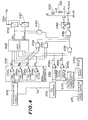
- the power regulation circuit 10 is connected to an electronic anti-skid control system 24 to supply a given constant voltage of electrical power to the latter.
- the anti-skid control system 24 is connected wheel r.p.m. sensors 22a, 22b and 22c to receive sensor signals respectively representative of driving and driven wheel speeds. Based on the sensor signals, the anti-skid control system 24 activates and deactivates electromagnetic actuators 26a, 26b and 26c through transistors Tr 2 , Tr 3 and Tr 4 .
- the electromagnetic actuators 26a, 26b and 26c control application and release of wheel cylinders in a hydraulic brake system for preventing vehicle wheels from skidding.
- the electromagnetic actuators 26a, 26b and 26c are connected to a power source, i.e., vehicle battery via a relay switc 20a.
- the power regulation circuit 10 is also connected to a fail-safe circuit 13.
- a monitor power supply circuit 12 which is, in turn, connected to the vehicle battery acting as a power source V B .
- the fail-safe circuit 13 includes a pair of comparators 14 and 16.
- the positive input terminsl (+) of the comparator 14 is connected to the power regulation circuit 10 via dividing resistor R 1 and to ground via dividing resistor R 2 .
- the negative input terminal (-) of the comparator 16 is connected to the power regulation circuit 10 and ground via the dividing resistors R 1 and R2 respectively.
- the positive input terminal (+) of the comparator 14 and the negative input terminal (-) of the comparator 16 thus receive the divided voltage V .
- the input voltage V a to the comparator 14 and 16 from the power regulation circuit can be calculated by the following equation:
- the negative input terminal (-) of the comparator 14 is connected to the monitor power supply circuit 13 via dividing resistor R 3 , and to ground via dividing resistors, R 4 and R 5 .
- the positive input terminal (+) of comparator 16 is also connected to the monitor power supply circuit 12 via the dividing resistors R 3 and R 4 and to ground via dividing resistor R 6 .
- the input voltages V b and V c respectively applied to the comparators 14 and 16 can be respectively expressed by the following equations: where r 3 is resistance value of resistor R 3 r 4 is resistance value of resistor R 4 r 5 is resistance value of the resistor R 5 E 1 is output voltage of the monitor power supply circuit.
- the comparators 14 and 16 are energized with voltage E 1 from the monitor power supply circuit 12.
- the comparator 14 is adapted to produce a HIGH level comparator signal when the signal voltage V a is larger than that of V b .
- the comparator 16 is adapted to produce a HIGH level comparator signal when the signal voltage V a is smaller than that of V .
- the output terminals of the comparators 14 and 16 are respectively connected to a base electrode of a transistor Tr via respective diodes D 1 and D 2 and a common resistor R 6 .
- the collector electrode of the transistor Tr l is connected to a fault indicator lamp 18 and, in turn, to a relay coil 20 which serves as a collector load.
- the anti-skid brake control system is constructed in per se known circuit construction as discloses in U.S. Patent 3,744,851 to Bruckhardt et al, for example.
- Other anti-skid control systems have been disclosed in British Patent Prepublications Nos. 2,061,435, 2,062,786 and 2,066,894.
- the disclosures in the above-referred publications are hereby incorporated by reference.
- the electronic anti-skid control system generally controls application and release of brake pressure in the wheel cylinder in order to control tread/road friction to near the maximum value.
- the anti-skid control system produces a control signal to be fed to the electromagnetic actuators 26a, 26b and 26c to control actuation of the fluid pressure in the wheel cylinder of the hydraulic brake system.
- the anti-skid control system can comprise a digital circuit including CMOS and/or TTL elements, or an analog circuit including an operational amplifier, comparators and so forth. Either of the digital and analog circuits would be influenced by variations in the power regulation circuit output voltage.
- the' allowable voltage variation of the power regulation circuit 10 is within the range 5.25V-a ⁇ E O ⁇ 5.25V+a, where a is the allowable voltage variation of the TTL circuit elements.
- the input voltage V a to the comparators 14 and 16 becomes greater than normal corresponding to the increase of the output voltage of the power regulation circuit.
- the input voltage V a becomes higher than the input voltage V b .
- the comparator 14 thus produces a HIGH level comparator signal.
- the HIGH level comparator signal of the comparator 14 is fed to the transistor Tr 1 via the diode D 1 and the resistor R 6 .
- the transistor Tr 1 is turned off in response to the HIGH level comparator signal from the comparator 14 to produce a bias voltage at the collector electrode thereof.
- the bias voltage of the transistor Tr 1 is fed to the indicator lamp 18 to turn the latter on.
- the relay coil 20 is energized by the bias voltage of the transistor Tr 1 to open the relay switch 20a.
- the electromagnetic actuators 26a, 26b and 26c are disconnected from the power source, i.e., from the vehicle battery, to be rendered inactive.
- the input voltage V a to the positive input terminal of the comparator 14 and the negative input terminal of the comparator 16 becomes lower than normal.
- the transistor Tr 1 is cut-off by the HIGH level comparator signal of the comparator 16 to turn on the indicator lamp 18 and energize the relay coil.
- the comparator signals of the comparator 14 and 16 are maintained at LOW level to keep the transistor Tr 1 ON.
- the indicator lamp 18 is maintained OFF and the relay coil 20 is deenergized to allow power supply to the electromagnetic actuators 26a, . 26b and 26c to make the anti-skid control system active.
- the comparator 14 and 16 in order to prevent the fail-safe circuit 13 from malfunctioning due to sudden significantly HIGH voltages, the comparator 14 and 16 must be designed to withstand even substantially HIGH voltages, i.e., voltages exceeding 12V. This will ensure the operation of the fail-safe system of the shown embodiment.
- the fail-safe circuit 113 comprises two pairs of comparators 114, 116 and 130, 132.
- the power regulation circuit 10 and ground are connected to positive input terminals (+) of the comparators 114 and 130 and to negative input terminals (-) of the comparators 116 and 132, via dividing resistors R 11 and R 12 respectively, as in the foregoing embodiment.
- the monitor power supply circuit 12 and ground are connected to the negative input terminal (-) of the comparator 14 and the positive input terminal (+) of the comparator 16 via the dividing resistors R 13 , R 14 and R 15 .
- the positive input terminal of the comparator 14 and the negative input terminal of the comparator 16 receive divided voltage V .
- the negative input terminal of the comparator 14 receives the divided voltage V b and the positive input terminal of the comparator 16 receives the divided voltage V c .
- the comparators 14 and 16 act similarly to the foregoing embodiment to turn on the transistor Tr 11 via the diodes D 11 and D 12 and the common resistor R 16 when the input voltage V a from the power regulation circuit 10 is out of a given range defined by the input voltage from the monitor power supply circuit 12 and resistors R13, R 14 and R 15 .
- the indicator 118 is turned on and the relay coil 120 is energized when the transistor is cut-off.
- the comparators l14 and 116 receive power from the monitor power supply circuit 12 for operation and, in turn, the comparators 130 and 132 receive power from the power regulation circuit 10.
- the comparator 130 and 132 are adapted to monitor the monitor power supply circuit 12 for malfunctions. As with the comparators 14 and 16, the positive input terminal of the comparator 130 and the negative input terminal of the comparator 132 receive divided voltage V a . The negative input terminal of the comparator receives the input voltage V b from the monitor power supply circuit 12 via the dividing resistors R 13 , R 14 and R 15 . Similarly, the divided voltage V c from the dividing resistors R 13 , R 14 and R 15 is applied to the positive input terminal of the comparator 132. The comparator 130 thus compares the input voltages V a and V b and produces a HIGH level comparator signal when the input voltage V a is larger than V b . On the other hand, the comparator 132 is adapted to produce a HIGH level comparator signal when the input voltage V a is less than V . c
- the comparators 130 and 132 are connected to the base electrode of a transistor Tr 110 via respective diodes D 13 and D 14 and a common resistor R 17 .
- the transistor Tr 110 is responsive to application of a HIGH level comparator signal via the resistor R 17 to turn OFF.
- the transistor Tr 110 is applied to the indicator lamp 118 and the relay coil 120.
- the indicator lamp 118 is turned ON and the relay coil 120 is energized.
- the fail-safe circuit l13 monitors not only the output voltage of the power regulation circuit 10 but also the output voltage of the monitor power supply circuit 12.
- Fig. 3 is a schematic block diagram of the second embodiment of the fail-safe system for the power regulation circuit according to the present invention.
- the fail-safe circuit 213 has substantially the same circuit construction as set forth with respect to the first embodiment.
- the fail-safe circuit 213 is connected to the monitor power supply circuit 12 to receive operational power for the. comparators.
- the anti-skid control system has substantially the same circuit construction as that disclosed with reference to Fig. 1.
- a monitor circuit 236 corresponding to the faul-safe circuit 113 of Fig. 2 is connected to the power regulation circuit 10 and the monitor power supply circuit 12.
- the monitor circuit 236 is adapted to monitor both of the input voltages E 0 and E 1 from the power regulation circuit 10 and the monitor power supply circuit 12 respectively.
- the monitor circuit 236 is connected to base electrodes of transistors Tr 210 and Tr 211 via respective resistors R 26 and R 27 . As in the foregoing embodiment, the transistors Tr210 and Tr 211 will be cut off when the corresponding one of the power regulation circuit 10 and the monitor power supply circuit 12 outputs an excessively high or low voltage in order to actuate the relay coil 220.
- Figs. 4 and 5 show one example of the fail-safe system which is applied for an anti-skid brake control system.
- a wheel rotation speed sensor 2131 is adapted to produce a pulse train with a frequency proportional to the wheel rotation speed.
- the pulse train is converted into an analog signal by a frequency-to-voltage converter (F/V converter) 2132, which analog signal V w has a voltage proportional to the wheel rotation speed.
- F/V converter frequency-to-voltage converter
- a differentiation circuit 2133 Based on the variation of the analog signal value, a differentiation circuit 2133 produces a signal a at a voltage representative of instantaneous wheel acceleration.
- the signal ⁇ w is fed to a wheel acceleration comparator 2134 which comprises first to fourth differential amplifiers 2314a to 2134d.
- the signal ⁇ w is inputted to the positive input terminals (+) of the first and second differential amplifiers 2134a and 2134b and to the negative input terminals (-) of the differential amplifiers 2134c and 2134d.
- the negative input terminals of the differential amplifiers 2134a and 2134b respectively receive reference voltages ⁇ 1 and a 2 corresponding to acceleration levels of l.OG and 0.5G.
- the positive input terminals of the differential amplifiers 2134c and 2134d receive reference voltages a3 and a4 respectively corresponding to acceleration levels of -1.OG and -1.5G.
- the outputs e 1 and e 2 of the differential amplifiers 2134a and 2134b will be HIGH and outputs e 3 and e 4 of the remaining differential amplifiers 2134c and 2134d will be maintained at LOW level.
- the output e 1 of the differential amplifier 2134a turns to LOW level and the output e 2 is maintained at HIGH level.
- the outputs of all the differential amplifiers 2134a to 2134d are LOW level.
- the signal value ⁇ w of the signal ⁇ w drops to a value less than the reference voltage ⁇ 3
- the output e 3 of the differential amplifier 2134c goes HIGH and the other output signals remain LOW.
- the outputs e 3 and e 4 both go HIGH.
- the outputs of the differential amplifiers 2134a to 2134d in relation to the wheel acceleration a are w summarized in the following table:
- a vehicle speed sensor 2135c produces a vehicle speed signal indicative of the vehicle speed.
- the vehicle speed signal is fed to a vehicle speed signal generator 2135 which is adapted to produce a reference signal Vc at a voltage related to vehicle speed and which changes at a rate related to vehicle acceleration.
- the reference signal Vc is fed to reference voltage generators 2135a and 2135b.
- the reference voltage generator 2135a produces a reference voltage Vc 1 having a value corresponding to 85% of the signal value of the reference signal Vc.
- the reference voltage generator 2135b produces a reference voltage Vc 2 having a value corresponding to 70% of the signal value of the reference signal Vc.
- the reference voltage generators 2135a and 2135b are respectively connected to positive input terminals of differential amplifiers 2136a and 2136b.
- the analog signal V representative of the wheel rotation speed is also inputted to the negative input terminals of the differential amplifiers 2136a and 2136b.
- the differential amplifiers 2136a and 2136b vary the level of the outputs E 1 and E 2 depending on the slippage of the wheel determined on the basis of the reference voltages Vc 1 and Vc 2 .
- the variation of the output level of the differential amplifiers 2136a and 2136b with respect to the variation of the analog signal V w . in relation to the reference voltages Vc 1 and Vc 2 is illustrated in the following table:
- the outputs e 1 to e 4 and E 1 and E 2 are fed to a logic circuit 21315.
- the logic circuit 21315 determines signal level of an inlet signal E v and an outlet signal A v according to the following chart:
- the brake system is provided with an inlet valve 21322 and an outlet valve 21323 in the hydraulic circuit.
- the inlet valve 21322 includes an inlet valve actuator 21316 and the outlet valve 21323 includes an outlet valve actuator 21317, as shown in Fig. 5.
- the inlet valve 21322 is connected to a brake master cylinder 21325 to receive a working fluid through a passage 21326 and is also connected to the wheel cylinder 21329 to apply the working fluid thereto.
- the master cylinder 21325 responds to depression of an associated brake pedal 21324 to increase the fluid pressure within passage 21326.
- the working fluid is thus fed to the wheel cylinder 21329 when a brake pedal 21324-is depressed and the inlet valve 21322 is opened.
- the inlet valve actuator 21316 is responsive to the HIGH-level inlet signal E to be energized and close the inlet valve.
- the outlet valve 21323 is a normally closed valve and is responsive to energization of the outlet valve actuator 21317 to open in response to the outlet signal A. When the inlet valve 21322 and the outlet valve 21323 are both closed, the fluid pressure applied to the wheel cylinder 21329 is maintained at a constant level.
- the outlet valve 21323 is connected to the brake master cylinder 21325 via a fluid pump 21327 and an one-way valve 21328.
- the outlet valve 21323 When the outlet valve 21323 is open the working fluid in the passage between inlet valve 21322 and wheel cylinder 21329 is fed back to the master cylinder 21325 through the fluid pump 21327 and the one-way valve 21328.
- the inlet and outlet valve actuators 21316 and 21317 are respectively operated by switches 21320 and 21321 which are turned on in response to the inlet and outlet signals E and A .
- the fail-safe operation is carried out after detection of errors in the anti-skid brake control.
- AND gates 2137 and 2138 are provided.
- the AND gate 2137 has an input terminal connected to the differential amplifier 2134d and an inverting input terminal connected to the differential amplifier 2134c.
- the output e 3 of the differential amplifier 2134c is LOW and the output e 4 of the differential amplifier 2134d is HIGH, therefore, if the AND gate 2137 outputs a HIGH signal, it means the anti-skid brake control system is malfunctioning.
- the differential amplifiers 2134a and 2134b to the AND gate 2138 via an input terminal and an inverting input terminal respectively, errors in the control system can be detected.
- the AND gates 2137 and 2138 produce HIGH level signals only when the acceleration comparator is malfunctioning.
- the output terminals of the AND gates 2137 and 2138 are connected to the SET input terminal S of an' R-S-type flip-flop 21312 via an OR gate 21311.
- the flip-flop 21312 produces a SET signal at its Q-output terminal to turn ON a transistor Tr 1 to illuminate a fault indicator lamp 21313 and stops producing a RESET signal at its Q-output terminal to turn OFF another transistor Tr 2 to deenergize a relay coil 21318 which opens a relay switch 21318a and thereby disables the anti-skid control operation of the inlet and outlet valve actuators 21316 and 21317.
- an AND gate 2139 is connected to the differential amplifiers 2136a and 2136b to receive the outputs E 1 and E 2 .
- One of the input terminals of the AND gate 2139 is an inverting input terminal connected to the differential amplifier 2136a.
- the AND gate outputs a HIGH-level signal when the output E 1 of the differential amplifier 2136a is LOW and the output E 2 of the differential amplifier 2136b is HIGH, which is not possible under normal circumstances.
- the AND gate is also connected to the SET terminal of the flip-flop 21312 via the OR gate 21311 in order to disconnect the anti-skid control system when such an erroneous combination of control signals is detected.
- Another AND gate 21310 is connected to the flip-flop 21312 via the OR .gate 21311 for fail-safe purposes.
- the AND gate 21310 is connected to the logic circuit 21315 to receive the outlet signal Av at one input terminal and the inlet signal E v at an inverting input terminal.
- the inlet signal E LOW and the outlet signal A HIGH it is not possible to have the inlet signal E LOW and the outlet signal A HIGH. Therefore, by detecting this condition, malfunction of the control system can be detected and by deactivating the relay coil 21318, the fail-sae operation can be performed.
- flip-flop 21312 should be RESET initially in order to enable automatic anti-skid control. This can be realized in any of a number of ways which will occur to those skilled in the art.
- errors in the anti-skid control system can be satisfactorily detected and fail-safe operation can be performed by disabling the control system.
- the fail-safe system according to the present invention can satisfactorily and successfully prevent the control system from failing even when the power regulation circuit therefor is damaged or malfunctions.
Landscapes
- Engineering & Computer Science (AREA)
- Transportation (AREA)
- Mechanical Engineering (AREA)
- Regulating Braking Force (AREA)
- Emergency Protection Circuit Devices (AREA)
- Protection Of Static Devices (AREA)
Applications Claiming Priority (2)
| Application Number | Priority Date | Filing Date | Title |
|---|---|---|---|
| JP152969/81 | 1981-09-29 | ||
| JP56152969A JPS5854830A (ja) | 1981-09-29 | 1981-09-29 | 車両用電子回路の電源監視装置 |
Publications (4)
| Publication Number | Publication Date |
|---|---|
| EP0075931A2 true EP0075931A2 (fr) | 1983-04-06 |
| EP0075931A3 EP0075931A3 (en) | 1986-02-05 |
| EP0075931B1 EP0075931B1 (fr) | 1989-02-01 |
| EP0075931B2 EP0075931B2 (fr) | 1992-12-30 |
Family
ID=15552102
Family Applications (1)
| Application Number | Title | Priority Date | Filing Date |
|---|---|---|---|
| EP82108983A Expired EP0075931B2 (fr) | 1981-09-29 | 1982-09-28 | Système de sécurité dans un circuit de régulation d'alimentation pour un circuit électronique d'automobile |
Country Status (4)
| Country | Link |
|---|---|
| US (1) | US4707758A (fr) |
| EP (1) | EP0075931B2 (fr) |
| JP (1) | JPS5854830A (fr) |
| DE (1) | DE3279416D1 (fr) |
Cited By (7)
| Publication number | Priority date | Publication date | Assignee | Title |
|---|---|---|---|---|
| EP0075932A2 (fr) * | 1981-09-28 | 1983-04-06 | Nissan Motor Co., Ltd. | Système de commande de freinage à antiblocage muni d'un dispositif de sécurité |
| EP0125660A2 (fr) * | 1983-05-17 | 1984-11-21 | Nissan Motor Co., Ltd. | Système de commande de freinage antiblocage avec système de sécurité sensible à une alimentation anormale |
| EP0179194A1 (fr) * | 1984-09-25 | 1986-04-30 | WABCO Westinghouse Fahrzeugbremsen GmbH | Dispositif de protection du circuit électronique d'un système antiblocage contre les surtensions |
| FR2650675A1 (fr) * | 1989-08-01 | 1991-02-08 | Teves Gmbh Alfred | Agencement de circuit permettant la surveillance d'un ensemble de plusieurs valves, notamment d'un circuit de freinage a regularite du glissement |
| US5176429A (en) * | 1989-12-01 | 1993-01-05 | Nissinbo Industries, Inc. | Failure detection circuit for anti-skid braking system |
| GB2284314A (en) * | 1993-11-27 | 1995-05-31 | Bosch Gmbh Robert | Regulator function monitoring in a motor vehicle |
| US7535739B2 (en) | 2004-02-24 | 2009-05-19 | Denso Corporation | Semiconductor switch |
Families Citing this family (15)
| Publication number | Priority date | Publication date | Assignee | Title |
|---|---|---|---|---|
| JPS59161342U (ja) * | 1983-04-12 | 1984-10-29 | ソニー株式会社 | 保護回路 |
| US4705508A (en) * | 1985-09-30 | 1987-11-10 | Regents Of The University Of Minnesota | Apparatus and method for rapid infusion of circulatory supportive fluids |
| US4812677A (en) * | 1987-10-15 | 1989-03-14 | Motorola | Power supply control with false shut down protection |
| US4983955A (en) * | 1988-11-28 | 1991-01-08 | Hendry Mechanical Works | Electric power supply circuit monitoring systems |
| US5648759A (en) * | 1994-02-02 | 1997-07-15 | National Semiconductor Corporation | Failsafe voltage regulator with warning signal driver |
| JP3752022B2 (ja) * | 1995-08-25 | 2006-03-08 | 株式会社デンソー | 故障診断機能付き電子制御装置 |
| US6208242B1 (en) * | 1997-10-24 | 2001-03-27 | Continental Teves Ag & Co., Ohg | Circuit configuration to monitor a regulated output voltage in a motor vehicle |
| US6144903A (en) * | 1998-08-03 | 2000-11-07 | Meritor Heavy Vehicle Systems, Llc | Electrical fault recognition system for vehicles |
| JP2001313368A (ja) * | 2000-04-28 | 2001-11-09 | Denso Corp | 集積回路 |
| US6624531B2 (en) * | 2001-10-09 | 2003-09-23 | Delphi Technologies, Inc. | Controller input voltage regulation by actuator power modulation |
| US8746812B2 (en) * | 2004-10-08 | 2014-06-10 | Marcia Albright | Brake control unit |
| FR2947227B1 (fr) * | 2009-06-25 | 2011-06-17 | Bosch Gmbh Robert | Systeme de freins hydrauliques a assistance hydraulique |
| EP3288806B1 (fr) * | 2015-04-29 | 2019-01-30 | New York Air Brake LLC | Système de contrôle et action d'émergence pour un frein de véhicule ferroviaire |
| JP6555167B2 (ja) * | 2016-03-25 | 2019-08-07 | 株式会社安川電機 | 電動機及びブレーキの解除方法 |
| JP7375572B2 (ja) | 2020-01-24 | 2023-11-08 | セイコーエプソン株式会社 | 物理量検出回路、物理量センサー、電子機器、移動体及び物理量センサーの故障診断方法 |
Citations (2)
| Publication number | Priority date | Publication date | Assignee | Title |
|---|---|---|---|---|
| FR2205430A1 (fr) * | 1972-11-03 | 1974-05-31 | Bosch Gmbh Robert | |
| US4246566A (en) * | 1978-05-09 | 1981-01-20 | Nippondenso Co., Ltd. | Malfunction diagnosing apparatus for electronic control system for vehicles |
Family Cites Families (11)
| Publication number | Priority date | Publication date | Assignee | Title |
|---|---|---|---|---|
| US3225257A (en) * | 1962-10-09 | 1965-12-21 | Burroughs Corp | High speed direct current voltage fault sensing, indicating and load protecting apparatus |
| US3394270A (en) * | 1965-02-05 | 1968-07-23 | Navy Usa | Plural input voltage comparing signal generator |
| DE1914765C2 (de) * | 1969-03-22 | 1982-11-11 | Teldix Gmbh, 6900 Heidelberg | Elektrische Steueranlage für ein blockiergeschützte Fahrzeugbremsanlage |
| DE1937123A1 (de) * | 1969-07-22 | 1971-02-18 | Daimler Benz Ag | Bremskraftregelung fuer Fahrzeuge,insbesondere Kraftfahrzeuge |
| US3813667A (en) * | 1973-05-29 | 1974-05-28 | Us Navy | Three-phase power disturbance monitor |
| JPS50161658A (fr) * | 1974-06-19 | 1975-12-27 | ||
| JPS516038A (en) * | 1974-07-02 | 1976-01-19 | Furukawa Electric Co Ltd | Hikaridensorono seizohoho |
| JPS5229938A (en) * | 1975-09-02 | 1977-03-07 | Pioneer Electronic Corp | Detection apparatus for the operation of electric machiens |
| US4049326A (en) * | 1975-11-14 | 1977-09-20 | Motorola, Inc. | Fail safe circuit for an anti-skid control apparatus |
| US4156280A (en) * | 1976-12-17 | 1979-05-22 | International Business Machines Corporation | Utility monitor for detecting and storing power line disturbances |
| GB1602898A (en) * | 1977-04-26 | 1981-11-18 | Suwa Seikosha Kk | Circuit for detecting a voltage |
-
1981
- 1981-09-29 JP JP56152969A patent/JPS5854830A/ja active Granted
-
1982
- 1982-09-24 US US06/423,186 patent/US4707758A/en not_active Expired - Lifetime
- 1982-09-28 DE DE8282108983T patent/DE3279416D1/de not_active Expired
- 1982-09-28 EP EP82108983A patent/EP0075931B2/fr not_active Expired
Patent Citations (2)
| Publication number | Priority date | Publication date | Assignee | Title |
|---|---|---|---|---|
| FR2205430A1 (fr) * | 1972-11-03 | 1974-05-31 | Bosch Gmbh Robert | |
| US4246566A (en) * | 1978-05-09 | 1981-01-20 | Nippondenso Co., Ltd. | Malfunction diagnosing apparatus for electronic control system for vehicles |
Cited By (14)
| Publication number | Priority date | Publication date | Assignee | Title |
|---|---|---|---|---|
| EP0075932A2 (fr) * | 1981-09-28 | 1983-04-06 | Nissan Motor Co., Ltd. | Système de commande de freinage à antiblocage muni d'un dispositif de sécurité |
| EP0075932A3 (en) * | 1981-09-28 | 1986-01-29 | Nissan Motor Co., Ltd. | Anti-skid brake control system with fail-safe arrangement |
| EP0125660A2 (fr) * | 1983-05-17 | 1984-11-21 | Nissan Motor Co., Ltd. | Système de commande de freinage antiblocage avec système de sécurité sensible à une alimentation anormale |
| EP0125660A3 (en) * | 1983-05-17 | 1988-01-13 | Nissan Motor Co., Ltd. | Anti-skid brake control system with fail-safe system responsive to abnormal power supply |
| US5129713A (en) * | 1983-05-17 | 1992-07-14 | Nissan Motor Company, Limited | Anti-skid brake control system with fail-safe system responsive to abnormal power supply |
| EP0179194A1 (fr) * | 1984-09-25 | 1986-04-30 | WABCO Westinghouse Fahrzeugbremsen GmbH | Dispositif de protection du circuit électronique d'un système antiblocage contre les surtensions |
| GB2236631A (en) * | 1989-08-01 | 1991-04-10 | Teves Gmbh Alfred | Circuit arrangement for monitoring the control circuitry of a plurality of valves |
| US5099198A (en) * | 1989-08-01 | 1992-03-24 | Alfred Teves Gmbh | Circuit configuration for monitoring the final stages of a plurality of valves |
| FR2650675A1 (fr) * | 1989-08-01 | 1991-02-08 | Teves Gmbh Alfred | Agencement de circuit permettant la surveillance d'un ensemble de plusieurs valves, notamment d'un circuit de freinage a regularite du glissement |
| GB2236631B (en) * | 1989-08-01 | 1993-06-16 | Teves Gmbh Alfred | Circuit arrangement for monitoring the control circuitry of a plurality of valves |
| US5176429A (en) * | 1989-12-01 | 1993-01-05 | Nissinbo Industries, Inc. | Failure detection circuit for anti-skid braking system |
| GB2284314A (en) * | 1993-11-27 | 1995-05-31 | Bosch Gmbh Robert | Regulator function monitoring in a motor vehicle |
| GB2284314B (en) * | 1993-11-27 | 1997-08-13 | Bosch Gmbh Robert | Regulator function monitoring in a vehicle |
| US7535739B2 (en) | 2004-02-24 | 2009-05-19 | Denso Corporation | Semiconductor switch |
Also Published As
| Publication number | Publication date |
|---|---|
| DE3279416D1 (en) | 1989-03-09 |
| EP0075931A3 (en) | 1986-02-05 |
| JPS5854830A (ja) | 1983-03-31 |
| JPH0373212B2 (fr) | 1991-11-21 |
| EP0075931B2 (fr) | 1992-12-30 |
| EP0075931B1 (fr) | 1989-02-01 |
| US4707758A (en) | 1987-11-17 |
Similar Documents
| Publication | Publication Date | Title |
|---|---|---|
| US4707758A (en) | Fail-safe system in a power regulation circuit for an automotive electronic circuit | |
| EP0147720B1 (fr) | Système de sécurité dans un système de commande de freinage à antiblocage pour véhicules automobiles | |
| US4656588A (en) | Anti-skid brake control system with a plurality of independently operative digital controllers | |
| US4701854A (en) | Method and system for performing fail-safe operation for anti-skid automotive brake control system having a plurality of controllers independently operable to others | |
| US6497303B1 (en) | Electric power steering system | |
| US4345796A (en) | Anti-skid brake control system for controlling the two pairs of diagonally opposed wheels of a motor vehicle | |
| EP0075932B1 (fr) | Système de commande de freinage à antiblocage muni d'un dispositif de sécurité | |
| EP0125660B1 (fr) | Système de commande de freinage antiblocage avec système de sécurité sensible à une alimentation anormale | |
| US5142474A (en) | Electronic control apparatus having a fail-safe mechanism for a vehicle | |
| GB2127507A (en) | Anti-skid brake system for a vehicle | |
| US5176429A (en) | Failure detection circuit for anti-skid braking system | |
| US4709341A (en) | Self-monitoring system for detecting error at output port during cold start of microprocessor system | |
| US11661042B2 (en) | Method for operating a rotational speed sensor in a vehicle, and sensor assembly | |
| US5243324A (en) | Method of detecting a fault in an automotive system | |
| US6111514A (en) | Solenoid fail-safe using current feedback as a diagnostic input | |
| US4753492A (en) | Monitoring arrangement for anti-skid automotive brake system | |
| JPH0790765B2 (ja) | アンチロックブレ−キ装置用故障検出回路 | |
| JP3634362B2 (ja) | アンチロック制御及び電子式制動力分散 | |
| US3911392A (en) | Failure/malfunction warning circuit for wheel slip control systems | |
| EP0369179A1 (fr) | Système de contrôle antiblocage | |
| US3944288A (en) | Skid control system for two-wheeled vehicles | |
| US5287085A (en) | Automatic test and connect electrical power system for anti-lock and conventional brake equipped trailers | |
| US11104314B2 (en) | Sensor circuit compensation for supply voltage transients | |
| US4035032A (en) | Skid control system for two-wheeled vehicles | |
| KR940011939A (ko) | 차량의 이상검출장치 |
Legal Events
| Date | Code | Title | Description |
|---|---|---|---|
| PUAI | Public reference made under article 153(3) epc to a published international application that has entered the european phase |
Free format text: ORIGINAL CODE: 0009012 |
|
| 17P | Request for examination filed |
Effective date: 19820928 |
|
| AK | Designated contracting states |
Designated state(s): DE FR GB |
|
| RAP1 | Party data changed (applicant data changed or rights of an application transferred) |
Owner name: NISSAN MOTOR CO., LTD. |
|
| PUAL | Search report despatched |
Free format text: ORIGINAL CODE: 0009013 |
|
| AK | Designated contracting states |
Designated state(s): DE FR GB |
|
| 17Q | First examination report despatched |
Effective date: 19860602 |
|
| R17C | First examination report despatched (corrected) |
Effective date: 19870318 |
|
| GRAA | (expected) grant |
Free format text: ORIGINAL CODE: 0009210 |
|
| AK | Designated contracting states |
Kind code of ref document: B1 Designated state(s): DE FR GB |
|
| REF | Corresponds to: |
Ref document number: 3279416 Country of ref document: DE Date of ref document: 19890309 |
|
| ET | Fr: translation filed | ||
| PLBI | Opposition filed |
Free format text: ORIGINAL CODE: 0009260 |
|
| PLBI | Opposition filed |
Free format text: ORIGINAL CODE: 0009260 |
|
| 26 | Opposition filed |
Opponent name: HELLA KG HUECK & CO. Effective date: 19891025 |
|
| 26 | Opposition filed |
Opponent name: ALFRED TEVES GMBH Effective date: 19891031 Opponent name: HELLA KG HUECK & CO. Effective date: 19891025 |
|
| PUAH | Patent maintained in amended form |
Free format text: ORIGINAL CODE: 0009272 |
|
| STAA | Information on the status of an ep patent application or granted ep patent |
Free format text: STATUS: PATENT MAINTAINED AS AMENDED |
|
| 27A | Patent maintained in amended form |
Effective date: 19921230 |
|
| AK | Designated contracting states |
Kind code of ref document: B2 Designated state(s): DE FR GB |
|
| ET3 | Fr: translation filed ** decision concerning opposition | ||
| PGFP | Annual fee paid to national office [announced via postgrant information from national office to epo] |
Ref country code: FR Payment date: 20010911 Year of fee payment: 20 |
|
| PGFP | Annual fee paid to national office [announced via postgrant information from national office to epo] |
Ref country code: GB Payment date: 20010926 Year of fee payment: 20 |
|
| PGFP | Annual fee paid to national office [announced via postgrant information from national office to epo] |
Ref country code: DE Payment date: 20011015 Year of fee payment: 20 |
|
| REG | Reference to a national code |
Ref country code: GB Ref legal event code: IF02 |
|
| PG25 | Lapsed in a contracting state [announced via postgrant information from national office to epo] |
Ref country code: GB Free format text: LAPSE BECAUSE OF EXPIRATION OF PROTECTION Effective date: 20020927 |
|
| REG | Reference to a national code |
Ref country code: GB Ref legal event code: PE20 Effective date: 20020927 |
|
| APAH | Appeal reference modified |
Free format text: ORIGINAL CODE: EPIDOSCREFNO |